Martin P.M. Handbook of Deposition Technologies for Films and Coatings, Third Edition: Science, Applications and Technology
Подождите немного. Документ загружается.


Characterization of Thin Films and Coatings 831
related to unoccupied p-states. ELNES is an ideal tool for verification of first principle
calculations of density of states. ELNES can be used to extract information related to the local
bonding/coordination environment, and the valence state of the absorbing atoms with a spatial
resolution of a single atomic column. EELS fine structure features are critically influenced by
the energy resolution of the whole system. One way to increase the energy resolution of EELS
is to reduce the energy spread of the primary electron beam. This can be accomplished using
an electron monochromator.
An electromagnetic lens is not an ideal lens and is therefore subject to aberrations. It is the lens
aberrations that limit the resolution of the HRTEM and STEM imaging as well as the
capability for high spatial chemical composition analysis. Two types of aberration are of
particular importance: spherical aberration and chromatic aberration [144–146]. It has been
known for a long time that magnetic lens aberration can be corrected using a multipole
magnetic lens. However, owing to difficulties related to the precise alignment of each part, a
usable corrector was not built until 1998. The development of fast computing capabilities and
computer-controlled alignment has led to dramatic developments over the past decade,
enabling aberration correctors to be developed for TEM and STEM. All such correctors are
based on assemblies of multipole magnetic lenses to compensate the phase shift of the electron
waves. For TEM imaging, the aberration corrector corrects the objective lens aberration and
thus makes the HRTEM image with sub-
˚
Angstrom resolution. For STEM imaging, the
aberration corrector corrects the electron probe forming lens aberration and thus makes the
formation of electron probe with a size of sub-
˚
Angstrom possible. Overall, a combination of
lens aberration corrector and electron monochromator will lead to sub-
˚
Angstrom spatial
resolution for imaging and ∼0.2 eV energy resolution for EELS [147].
With much improved high-spatial and high-energy resolution, tremendous progress has been
made on the extension of aberration-corrected TEM and spectroscopy to the analysis of
materials at or near realistic environmental conditions: the aberration-corrected environmental
transmission electron microscope (ETEM). The ETEM offers the capability of studying the
key issues of scientific/technological interest, including the real-time observation of catalytic
processes, phase transformation, phase nucleation and growth, mass transport and coarsening
processes across the domain of solid–gas, solid–solid, and solid–liquid, and oxidation and
reduction processes at elevated temperature and pressure.
Thin sections for TEM can be prepared by a range of methods involving a variety of
specialized tools. These methods include one or a combination of the following steps:
microtoming, mechanical polishing, dimpling, electropolishing, tripod polishing, ion-beam
thinning, and FIB cutting. FIB cutting is a relatively new and very well-controlled way for the
preparation of TEM specimen, especially if one seeks a site-specific sample preparation.
However, one of the drawbacks associated with the FIB-prepared TEM sample is the ion beam
damage and the contamination of the specimen by both the Ga ion and the Pt coatings. For thin
film analysis, the structure of the thin film as well as the interface structure between the film
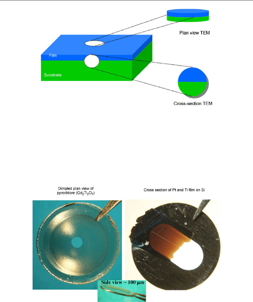
832 Chapter 16
Figure 16.54: Schematic drawing showing preparation of thin section of TEM specimen from a
sample with a thin film deposited on a substrate. The specimen can be prepared both either
cross-sectional view or plan view. A cross-sectional specimen can be prepared from different
directions to observe the specimen through different zone axes.
and the substrate can be analyzed either in plan view or in cross-sectional view as
schematically illustrated in Figure 16.54. Two optical images showing two thin-section TEM
samples are presented in Figure 16.55. One sample was prepared by dimpling of a thin section
with a thickness of about 100 m, followed by Ar ion beam thinning to obtain perforation at
Figure 16.55: Optical images of two TEM specimens. Left: The sample is prepared by dimpling
and followed by ion beam thinning to make the perforation at the center of the specimen. Note
that the diameter of the specimen is 3 mm and the side view shows the thickness of the sample at
the outer rim as ∼ 100 m. Right: The image shows a cross-sectional TEM sample mounted on a
molybdenum ring. The sample was prepared by tripod polishing. The central bright line is due to
the glue used in making the sample.
Characterization of Thin Films and Coatings 833
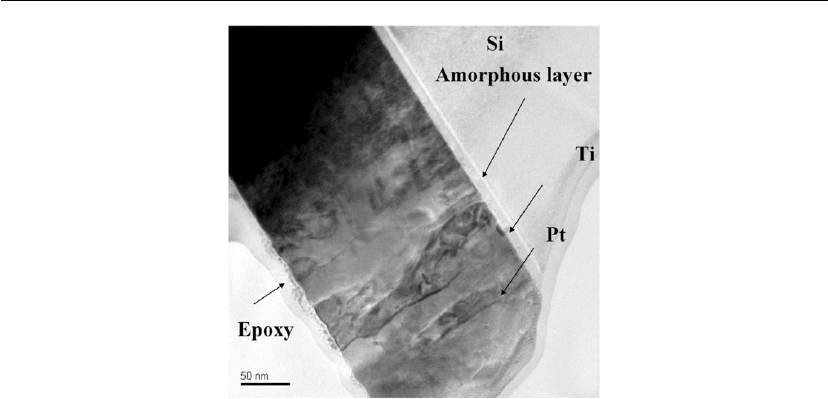
Figure 16.56: Cross-sectional TEM image of the Pt/Ti metal film coated on Si. Note the
amorphous layer of silicon oxide sandwiched between the crystalline Si and the Ti film. This image
shows that the mass-thickness contrast mechanism resulting in much darker contrast from Pt
film. Note that the internal features within the Pt film are also revealed by the diffraction contrast
mechanism.
the center of the disk. Another cross-sectional TEM specimen with Ti/Pt metal film deposited
on Si was prepared by tripod wedge polishing followed by slight Ar ion polishing.
16.5.3.1 Examples
In this section, we provide specific examples that relate to thin film analysis. A bright field
cross-sectional view of Pt and Ti metal films coated on a Si wafer is shown in Figure 16.56.In
the image the Pt film appears darker than the Ti film, owing to the high Z of Pt relative to
Ti (z contrast mechanism). Fine structural contrast features in the Pt film are related to
diffraction contrast and show that the Pt film is not a single crystalline film.
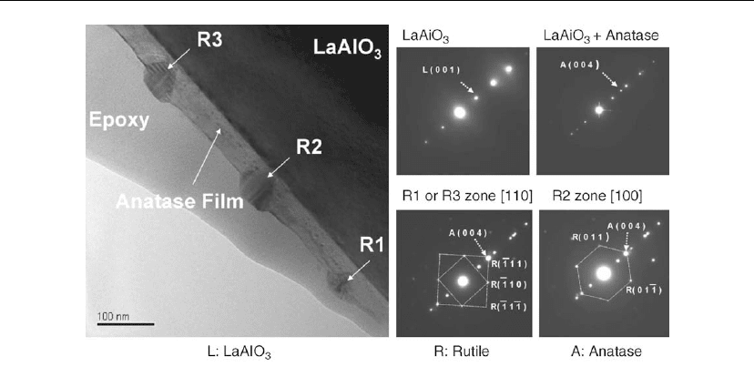
A cross-sectional TEM image showing a thin film of TiO
2
anatase deposited on an LAO
(LaAlO
3
) substrate is shown in Figure 16.57 [148]. This bright-field TEM reveals the
existence of TiO
2
rutile inclusions in the thin film and selected area electron diffraction
(SAED) can be used to determine the relative orientation of these inclusions with respect to the
film as well as the LAO substrate.
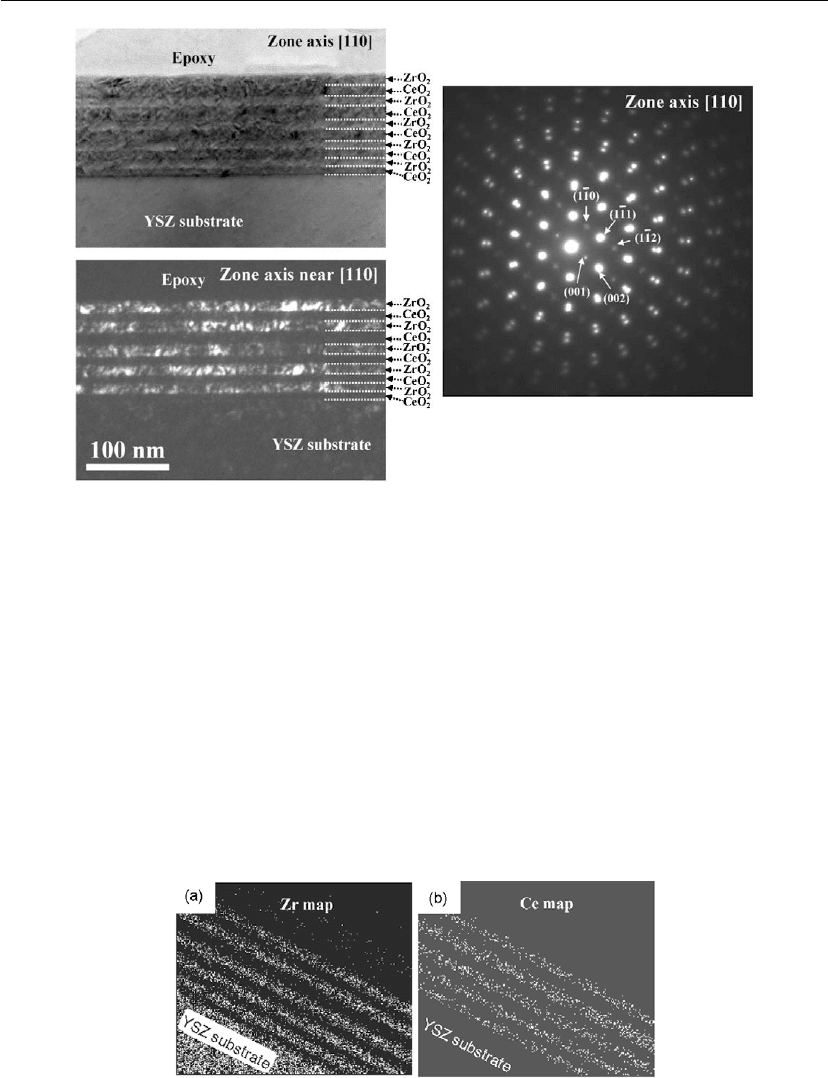
A combination of bright-field images, dark-field images, and SAED can also be used to
illustrate fine structural features. This is vividly illustrated in Figure 16.58 for the case of
multilayer alternating thin films of CeO
2
and ZrO
2
deposited on YSZ. The dark-field image
reveals the defective structural nature of the film, while the diffraction pattern clearly
demonstrates that all the film layers are in good epitaxial relationship. EDXS elemental
834 Chapter 16
Figure 16.57: Cross-sectional TEM image of anatase film deposited on LaAlO
3
substrate. Note
the formation of rutile inclusions in the anatase film. Electron diffraction was used to identify the
relative orientation of the rutile inclusion with respect to the anatase film. R3 and R1 have the
same orientation, while R2 possesses another orientation with respect to the anatase film [148].
mapping can also be used to map the distribution of the elements in the film and this is
demonstrated in Figure 16.59 for the case of the multilayer films shown in Figure 16.58
[149].
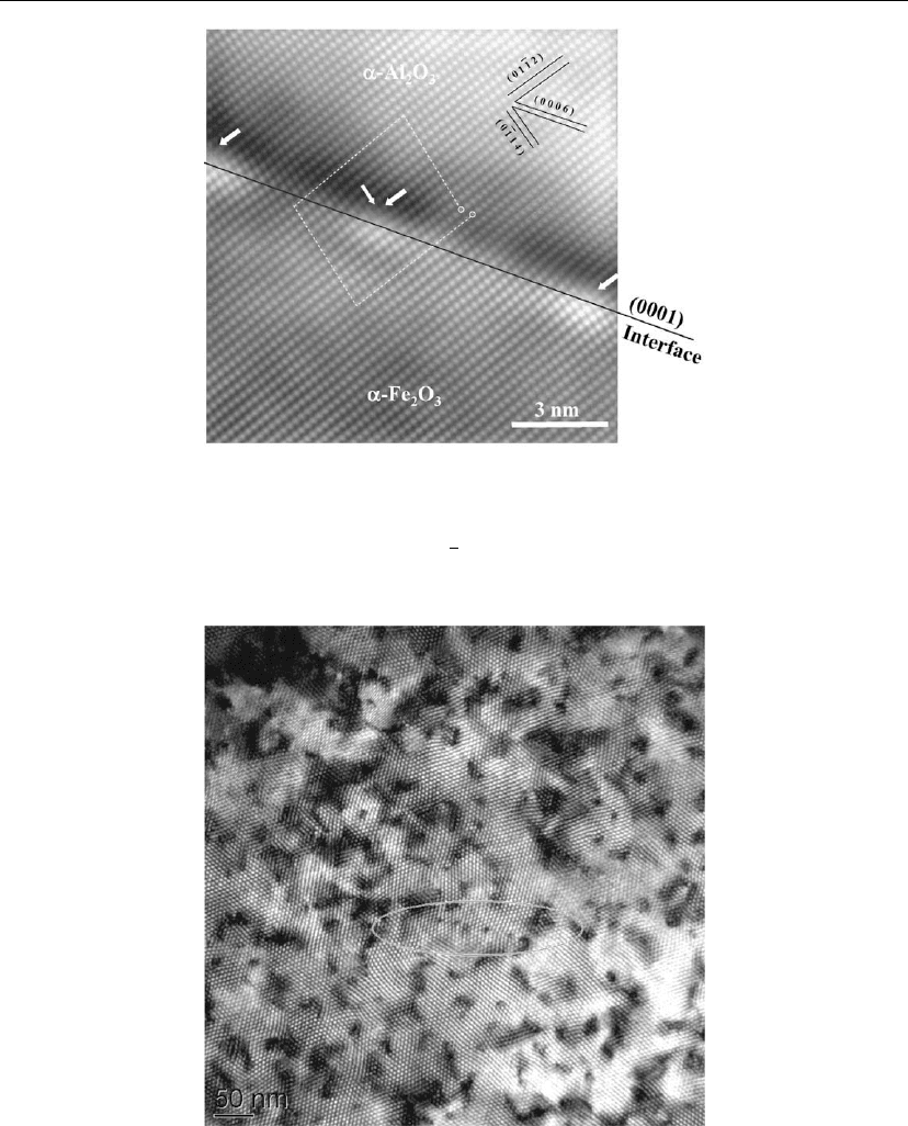
For thin films deposited on a substrate, the TEM sample can be prepared both in a plan view
and in a cross-sectional view. Figures 16.60 and 16.61 illustrate such an example for the case
of Fe
2
O
3
film deposited on Al
2
O
3
substrate [150]. The interface structure is observed in the
cross-sectional view using HRTEM imaging (Figure 16.60). Interface periodic mismatch
dislocations can be clearly seen and the Burgers vector of the dislocation can be determined
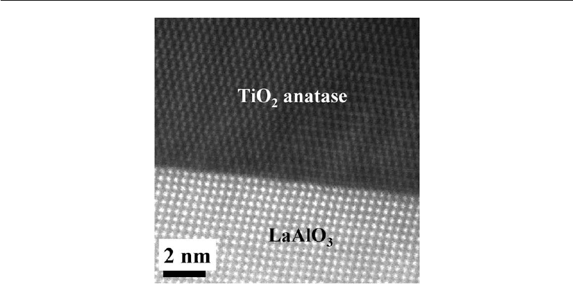
based on the HRTEM imaging. For the plan-view imaging, owing to the isostructural nature of
both Fe
2
O
3
and Al
2
O
3
and lattice constant differences, the Moir
´
e pattern dominates the image
contrast (Figure 16.61). The distribution of the dark contrasted dots represents the distribution
of the interface mismatch dislocations across the whole interface. The power of
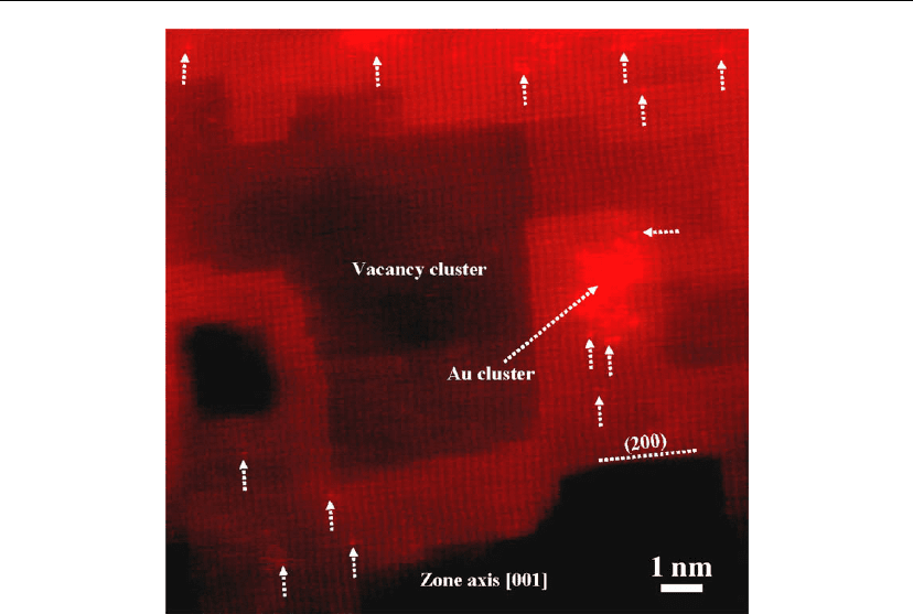
STEM-HAADF Z-contrast imaging on the direct revealing of the interface structure across a
film and the interface is illustrated in Figure 16.62, for which TiO
2
was deposited on LAO.
Because the STEM-HAADF image contrast is directly related to Z
2
, the large Z element will
appear as a bright dot. Therefore, the La column will be much brighter. This contrast provides
a way to judge the interdiffusion of atomic species between the film and the substrate.
Apparently, the interface is very sharply defined for the case of TiO
2
on LAO. The single
atomic column imaging power of STEM-HAADF is also clearly demonstrated for the case of
Characterization of Thin Films and Coatings 835
Figure 16.58: Cross-sectional TEM image of alternating ZrO
2
/CeO
2
films deposited on YSZ
substrate. The layered structured was revealed by both bright-field (left top) and dark-field (left
bottom) images. The epitaxial orientation relationship is revealed by the selected area electron
diffraction (right) [149].
Au implanted into MgO substrate, as shown in Figure 16.63, through vacancies produced by
Au irradiation in MgO. HAADF-STEM imaging provides direct evidence on the clustering of
vacancies in excess of Au atoms to form quantum antidots at the immediate neighborhood of
the Au clusters, leading to a spatially associated Au nanocluster and the quantum antidots.
The antidots show a terraced layer structure and are typically faceted along MgO(100).
Figure 16.63 also directly reveals that Au atom substitutes for the Mg atom lattice position
[151].
Figure 16.59: Cross-sectional TEM EDXS elemental mapping showing the Zr and Ce distribution
in an alternating ZrO
2
/CeO
2
films deposited on YSZ substrate [149].
836 Chapter 16
Figure 16.60: Cross-sectional HRTEM image revealing the structure of the misfit dislocations
across Al
2
O
3
and Fe
2
O
3
. A Burgers circuit was drawn around one of the dislocations and it gives
a projected magnitude of the Burgers vector =|
1
2
[
¯
1010]|=0.41 nm. The image was taken from
[
¯
2110] zone axis [150].
Figure 16.61: Plan-view TEM image revealing the distribution of the interface mismatch
dislocations in two dimensions (typically the black dots) when Fe
2
O
3
film was deposited on
Al
2
O
3
substrate. The regular ‘lattice-like’ pattern is a Moir
´
e pattern due to the same structure of
Al
2
O
3
and Fe
2
O
3
, epitaxial growth, and slightly different lattice constant [150].
Characterization of Thin Films and Coatings 837
Figure 16.62: STEM-HAADF cross-sectional view, showing the interface between TiO
2
thin film
and LAO substrate.
Strengths:
High spatial resolution for structural information, crystallography, chemical
composition, atomic charging and bonding information.
Capable of analysis using a tiny amount of sample.
At some degrees, a direct tool for visualization.
Elemental analysis and mapping.
Z-contrast STEM imaging to obtain atomic species distribution.
Chemical state analysis by EELS.
Limitations:
Requires vacuum.
Sample preparation is tedious and artifacts are introduced during sample preparation.
Electron beam modification of the specimen (beam damage).
Strong dependence of image contrast on the imaging condition.
838 Chapter 16
Figure 16.63: STEM-HAADF image of Au implanted in MgO, showing that the dark-contrasted
regions are the vacancy clusters. Note the faceting of the vacancy cluster at the (001) planes as
well as the thickness change along the electron beam direction [151]. The arrows identify the Au
clusters.
16.5.4 Electron Diffraction (LEED and RHEED)
S. V. N. T. Kuchibhatla
For many decades, electron diffraction has been an indispensable technique for understanding
the crystal structure of surfaces, overlayers, and thin films [136] and is widely used as a tool
for monitoring the quality of epitaxial films during growth. Both low-energy electron
diffraction (LEED) and reflection high-energy electron diffraction (RHEED) are conceptually
similar to XRD for the bulk crystal structure determination. The fundamental difference
between the electron diffraction (ED) techniques and XRD is in the much lower penetration
depths in the former case. While the electron penetration depth is confined to the order of 2–4
monolayers (1–3 nm) the X-rays can penetrate through the bulk of a crystal (up to ∼10
5
nm)
[6]. LEED plays a crucial role in understanding the surface structure, in particular overlayer
structure from adsorbates, surface relaxation, and reconstruction. Excellent surface sensitivity
Characterization of Thin Films and Coatings 839
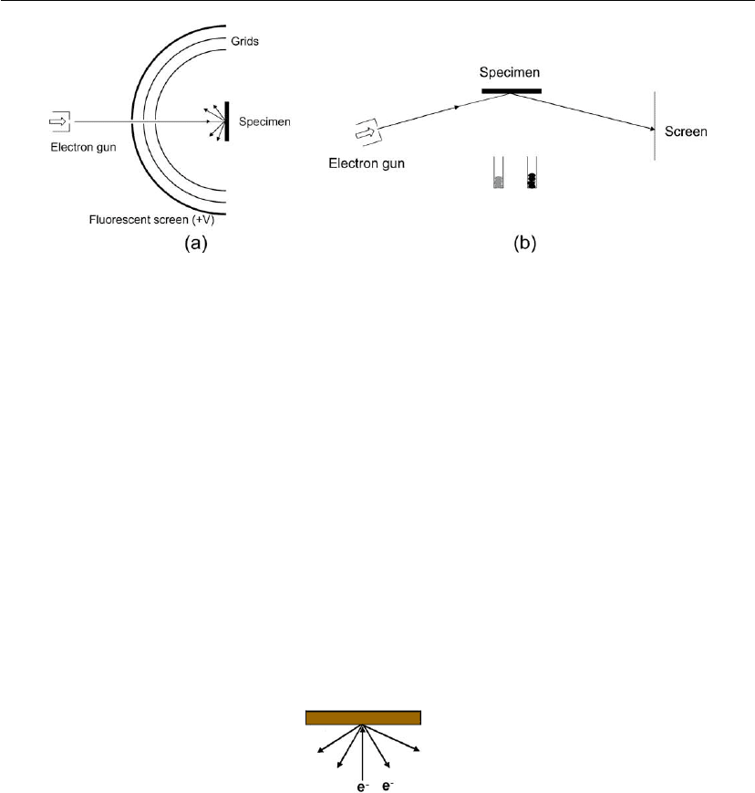
Figure 16.64: Typical instrument configuration for (a) LEED, and (b) RHEED.
and the ease with which the instrument can be used to monitor the in situ growth make
RHEED important in thin film research.
The Techniques
Typical instrument configurations for LEED and RHEED are shown in Figure 16.64. The
main differences between LEED and RHEED are beam energy and the scattered electron
path. While the LEED uses perpendicular incidence and backscattered electrons, RHEED
uses glancing incidence (≤3
◦
) and forward scattered electrons. Owing to the backscattered
geometry, LEED instrumentation is generally difficult to incorporate for monitoring in situ
growth. Hence, RHEED with no physical interference with the deposition process
became a more popular technique during molecular beam epitaxy (MBE) growth of thin
films.
16.5.4.1 Low-Energy Electron Diffraction
The position and intensity of diffraction peaks can be used to understand the structural
characteristics of the surface or overlayer under investigation and LEED instrumentation can
be used to obtain both these components as a function of electron energy. The basic LEED
set-up consists of an electron source, usually producing an electron beam 1 mm in diameter
and aligned perpendicular to the sample surface, a series of hemispherical grids oriented with
their origin at the sample surface, and a phosphor screen held at high positive potential. The
hemispherical grids are placed at different potentials to provide a field-free path to the
diffracted electrons and to allow only the elastically scattered electrons. The screen is kept at
840 Chapter 16
high potential (several kilovolts) to show visible fluorescence when the electrons strike the
screen. These fluorescent spots from various diffracted beams will result in a periodic
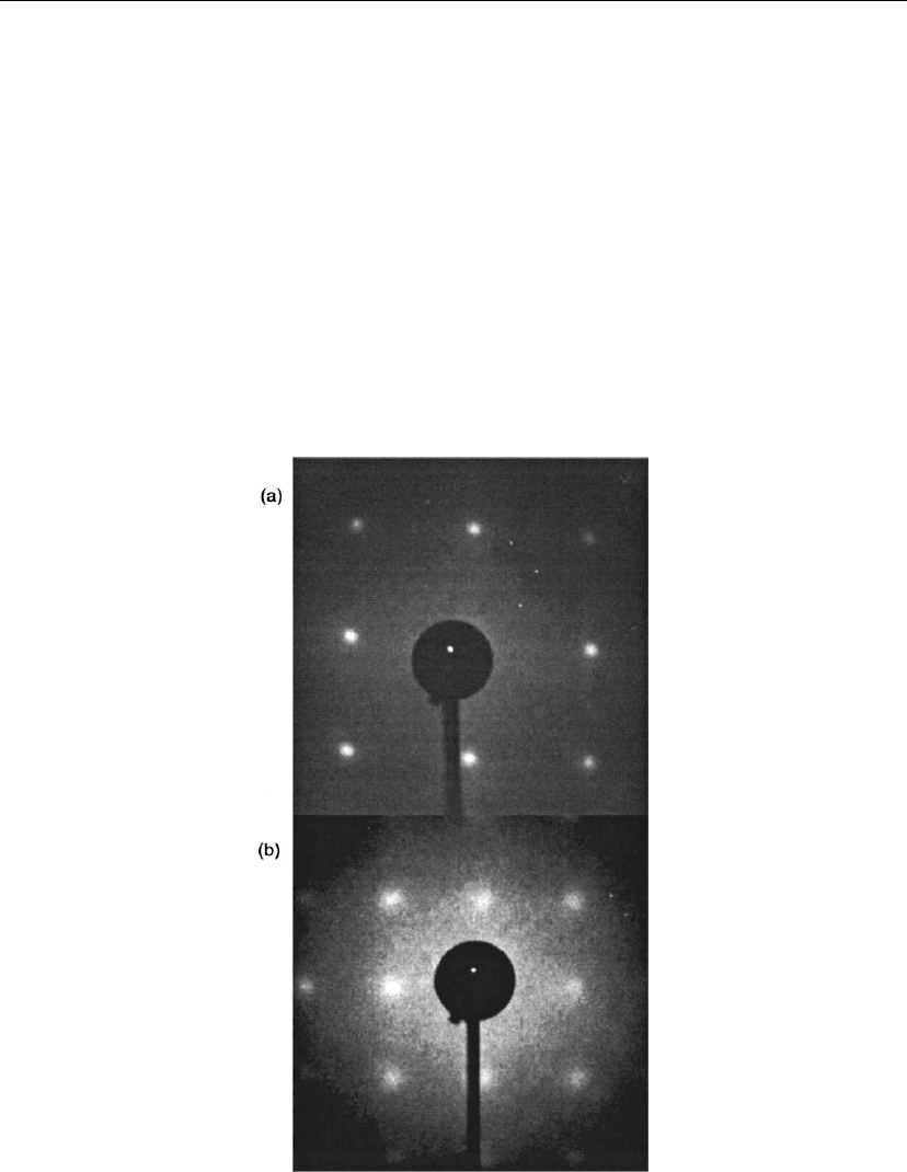
diffraction pattern, which can be captured with the help of a CCD camera.
LEED is often used in two qualitatively different modes, one to determine or verify the
symmetry of the surface and the second to determine the surface structure in some detail. The
diffraction spots seen in a LEED pattern (Figure 16.65) provide information about the
symmetry of the surface structure of the sample (they do not directly provide information
about the actual atomic positions) [152]. LEED is frequently used in this qualitative mode to
verify sample surface cleanliness, surface orientation, and the presence of ordered adsorbate
layers. Photometric measurements on the phosphor screen or a Faraday cup (adjustable to
follow changes in the diffracted beam position with changing primary electron energy) can be
used to determine the intensity of the diffraction spots as a function of incident beam energy.
Figure 16.65: Typical LEED patterns of (a) STO (001) substrate (∼98 eV incident beam), and (b)
CeO
2
(001) film deposited on STO at 650
C(∼165 eV incident beam) [152].
