Litton C.W., . Reynolds D.C., Collins T.C. Zinc Oxide Materials for Electronic and Optoelectronic Device Applications
Подождите немного. Документ загружается.

At high temperatures, the ZnO growth is preferable. In fact, it has been concluded that the
growth temperature for both ZnO buffer and GaN should be the same.
[8]
In this case, the
ZnO films have been grown by pulsed laser ablation of a solid ZnO target in oxygen
ambient on fused silica substrates. An ArF excimer laser with a wavelength of 193 nm,
a 250 mJ pulse energy and a 10 Hz repetition was used to deposit films. The substrate
temperature was kept at 600
C.
[9]
On this ZnO buffer layer, the GaN has been deposited
by a liquid-target pulsed laser technique. The flow rate of NH
3
and pressure in the chamber
were 20 sccm and 1 mbar, respectively. The same substrate temperature for the deposition
of GaN was maintained. If the substrate temperature is less than 550
o
C, the grown GaN
films are either amorphous or polyc rystalline. Columnar growth has proved to be highly
important for device applications.
[3]
An attempt to deposit GaN in N
2
atmosphere instead
of NH
3
was unsuccessful.
[9]
The deposition temperature of the PLD technique is much
lower than that of MOVPE, hence, it can be speculated that the optical grade GaN film can
be grown by this technique for device applications.
Wang et al.
[10]
prepared GaN layers on sapphire using ZnO buffer layers by the PLD
technique. The ZnO and GaN targets were prepared using commercially available
powders. The ZnO powder was pre-sintered at 900
CinO
2
ambient for 2 h, from which
a 2 cm diameter pallet was made and the GaN powder was also sintered at 800
C in the
presence of N
2
flow in a similar manner. A Nd:YAG pulsed laser, with a wavelength of
266 nm, a fluence of 0.8 J cm
2
per pulse and a repetition rate of 5 Hz, was employed for
deposition of ZnO and GaN layers at 800
C on sapphire substrates.
Room temperature layer by layer GaN growth by PLD on atomically flat ZnO (0001
)
substrate was demonstrated by Kobayashi et al .
[11]
To obtain an atomically flat
ZnO surface, ZnO (0001
) was annealed at 1150
C in air. During annealing, the ZnO
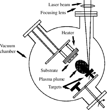
Figure 9.1 A schematic diagram of a pulsed laser deposition system. Reprinted from R. D.
Vispute, V. Talyansky, R. P. Sharma, S. Choopun, M. Downes, T. Venkatesan, K. A. Jones, A. A.
Iliadis, M. Asif Khan, and J. W. Yang, Growth of epitaxial GaN films by pulsed laser deposition,
Applied Physics Letters, 71, 102. Copyright (1997), American Institute of Physics
Growth of GaN/ZnO 223
substrates were kept in a ceramic ZnO box in order to suppress desorption of Zn atoms
from the ZnO surface and maintain the surface stoichiometry. GaN growth by PLD at room
temperature was conducted with the background pressure 5 10
10
Torr, and Ga metal
target (99.9999% purity) was irradiated with a KrF excimer laser (l ¼248 nm, t ¼20 ns),
having an energy density of 3.0 J cm
2
and pulse repetition rate of 10 Hz. As a nitrogen
source, a radio frequency (RF) plasma radical generator, which was operated at 360 W
with a N
2
pressure of 2.0 10
5
Torr, was used.
Ueda et al.
[12]
prepared ZnO films by PLD using a 248 nm KrF excimer laser with
a pulse duration of 20 ns and a repetition rate of 5 Hz. The partial pressure of oxygen was
0.01 Torr at 550
C. The streaky reflection high energy electron diffraction (RHEED)
pattern indicated a smooth layer with good atomic ordering rather than a spotty (indicative
of three-dimensional growth) or ring pattern (indic ative of polycrystalline growth) of RF
sputtered ZnO, as repor ted by others. Thick GaN layers were grown by using the HVPE
technique on pulsed laser deposited ZnO buffer layers on sapphire. GaCl
3
and NH
3
were
the source materials. In order to form GaCl
3
, HCl was passed over liquid Ga held at a high
temperature. The production rate of GaCl
3
was controlled by the temperature of the Ga
boat and HCl flow rate. The growth was performed at 1000
C at a V/III ratio of 500 and
the growth rate was 10 mmh
1
.
[12]
As soon as the required substrate temperature was
reached, GaN growth was started immediately to prevent thermal desorption of the ZnO
buffer layer from the sapphire substrate. The large difference in thermal expansion
coefficient between these compounds (ZnO, 2.9 10
6
K
1
; GaN, 5.6 10
6
K
1
; and
Al
2
O
3,
7.5 10
6
K
1
) must be kept in mind.
Detchprohm et al.
[13]
used sput tered ZnO on sapphire as buffer layers for GaN epitaxy.
A 10 cm diameter ZnO ceramic disk was used as target and Ar or O
2
was employed as
sputtering gas. Prior to deposition of ZnO, the chamber was evacuated to 10
5
Torr and
then the chamber pressure was maintained at 0.13 and 0.4 Torr for Ar and O
2
, respectively.
The discharging input and reflecting powers were 200 and 20 W, respectively, for both
gases. The ZnO growth rates were about 150 and 5 nm h
1
for Ar and O
2
, respectively. The
ZnO growth was performed at room temperature. The sputtered ZnO was not annealed
prior to deposition of GaN otherwise it would have decomposed according to the authors.
The GaN films were deposited by the HVPE technique. The Ga boat temperature was kept
at 850
C for the formation of GaCl
3
.
Molnar et al.
[14]
also used the HVPE technique to grow GaN thick templates by
employing ZnO as a buffer layer (Figure 9.2). The HVPE is useful to grow thick but
not necessarily large area GaN samples. GaN samples grown by this technique are of
considerable interest for follow up epitaxial growth because of reducing defect concen-
tration, as the film thickness increases. HCl used in the preparation process of GaN is
corrosive and affects the deposition system adversely. For this growth, GaCl, AlN and ZnO
were used to treat the substrates prior to growth of GaN. GaCl was synthesi zed by mixing
HCl and liquid Ga metal at 800–900
C and then it was passed down the reactor tube to
the substrate where it was allowed to react with NH
3
. Either ZnO or GaCl treated GaN on
sapphire samples showed highly transparent films, fewer hexagonal islands, and did not
show any polycrystalline nature.
Gu et al.
[15]
extensively studied the role of ZnO while depositing GaN by the HVPE
method. They observed that the thin ZnO prelaye r disappeared between the sapphire and
GaN. The reason is that ZnO is thermodynamically unstable in the presence of reducing
224 Growth and Characterization
agents coming from the source materials in the HVPE system. Gu et al. have used two
20 nm-thick ZnO samples deposited on sapphire, one annealed at 1050
C for 10 min in N
2
ambient and the other unannealed. The unannealed sample was dipped into HCl to dissolve
any ZnO film. The X-ray photoelectron spectroscopy (XPS) analysis showed no residual
ZnO or any other compound formed with sapphire. However, the annealed one, after
dipping in HCl, showed traces of ZnAl
2
O
4
by XPS analysis, which is the same as standard
compound ZnAl
2
O
4
. One can conclude that ZnAl
2
O
4
might form and may act as
nucleation centers for GaN growth. The authors have attempted to confirm the aforemen-
tioned results by using a supportive technique such as X-ray diffraction (XRD); however,
it is very difficult to trace this compound in thin layers so they did the analysi s on a
200 nm-thick sample annealed in air for 30 h that avoided any ambiguity. The rocking
curve line width of (0002) of GaN grown on sapphire was 700 arcsec, compare d with
400–500 arcsec for samples grown with ZnO buffer layer. The carrier concentration was
1 10
16
cm
3
for 20 nm-thick ZnO buffered GaN samples. The ZnAl
2
O
4
may promote
nucleation centers, in order to get growth and reduce lattice mismatch to GaN.
Building on the earlier investigations of Hamdani et al. on as-received ZnO sub-
strates,
[16]
Gu et al.
[17]
thoroughly studied ZnO substrates with O and Zn polarity prior to
GaN thin film deposition and developed a method to render the surfaces atomically flat
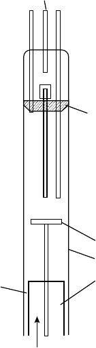
Ga-boat flow
NH
3
nozzle
Main carrier
Ga boat
Rotatable platen
Liner
Dump tube
Counterflow
Exhaust
900ºC
1000–
1100ºC
Figure 9.2 HVPE reactor for GaN growth. Reprinted from R. J. Molnar, et al., Growth of
gallium nitride by hydride vapor-phase epitaxy. J. Cryst. Growth, 178, 147. Copyright (1997)
with permission from Elsevier
Growth of GaN/ZnO 225
and damage free. ZnO substrates were annealed at 1050
C in air for 3 h in order to
improve the quality of the surface, which showed full width at half-maximum (FWHM) of
0.576 arcmin for the (0002) X-ray rocking curve, FWHM of 0.7 meV for the photo-
luminescence exciton peak, and surface roughness of 0.6 nm using atomic force micros-
copy (AFM). The unannealed and annealed ZnO substrates at temperature less than
1050
C showed rough surfaces, terraces, and scratches on the surface. GaN thin films
were prepared on both O and Zn face ZnO substrates usin g the RF plasma-enhanced
nitrogen MBE technique.
[18]
GaN films were also grown on ZnO substrates by reaction of
Ga and NH
3
at 760
C by employing either GaN or AlN buffer layer grown at lower
temperature by use of RF nitrogen source. For the growth of GaN films on ZnO substrates
with the MBE technique, Ga was supplied from a Knudsen cell, and filtered and purified
NH
3
was fed through the chamber by an injector retained at 300
C to prevent liquid NH
3
formation. During the growth, the chamber pressure was maintained at 2–5 10
5
Torr.
[18]
Similar approaches for ZnO substrate treatment
[19,20]
were reported using higher
annealing temperature in air. Ohgaki et al. annealed four different orientations of ZnO
substrates covered with single crystalline Y-stabilized ZrO
2
(YSZ) plate to prevent
evaporation of Zn.
[19]
After annealing at 1200
C for 2 h with the YSZ plate, all the
scratches were removed. Particularly step-and-terrace in the c(þ) and () - face were
observed, having surface roughness of 0.5 nm using AFM. On the other hand, a- and
m-ZnO showed a stripe pattern having surface roughness of 67 nm using AFM . GaN
films were grown on ZnO and low-temperature nearly lattice matched 30 nm-thick InGaN
buffer layer by MBE. The growth was initiated by simultaneously exposing the ZnO
surface to incident Ga (Ga and In) and N fluxes, which prevented nitridation and
metallization of the ZnO surface. Most of the growth experiments with GaN/ZnO
structures were conducted at low temperatures since the grown GaN films at higher
temperatures peel off from the ZnO substrate.
[21]
GaN on low-temperature InGaN buffer
layer was grown at 800
C. To prevent phase separation of the InGaN layer, the Ga and N
fluxes were supplied to the film surface while increasing the temperature from 550 to
800
C. In the case of epi-ZnO films, Heinze et al. performed in-situ annealing following a
low-temperature ZnO buffer layer growth at 900
C under t-B uOH and N
2
O atmosphere
with N
2
carrier gas to achieve smooth and clean surfaces and then high temperature ZnO
growth was performed increasing the growth temperature to 800900
C.
[20]
Oxygen-face
ZnO substrates grown by the liquid solution method (CrysTec GmbH, Berlin, Germany)
were annealed at 1100
C for 15 min in the ZnO box with a high amount of ZnO powder.
After the annealing process, surface roughness using AFM was 0.5 nm, which is the height
of a bilayer along the c-axis length. FWHM of the XRD rocking curve at the (0002)
reflection of the untreated samples was 220 arcsec, while the annealed one was 35 arcsec.
In terms of electrical characterization, the charge carrier density increased from 3.1 10
13
cm
2
in the as-grown sample to 3.8 10
14
cm
2
in the annealed sample. The carrier
mobility slightly decreased from 96.5 to 77.8 cm
2
V
1
s
1
, respectively.
[20]
Matsuoka et al.
[22]
used degreased and etched ZnO substrates to grow thin GaN films by
MOVPE. Until attaining the required growth temperature, a nitrogen flow was maintained
in the chamber, then ammonia and group III sources were allowed into the MOVPE
chamber. A vertical cold walled MOVPE reactor was used for the growth of InGaN and
InGaAlN epitaxial layers. The sources were trimethylindium (TMI), triethylgallium
(TEG), trimethylaluminum (TMA), and purified ammonia. The incorporation of In was
226 Growth and Characterization
increased by reducing the substrate temperature from 800 to 500
C. This is due to the
much higher vapor pressure of In compared with that of Ga. The typical ammonia flow rate
was 20 l min
1
. The growth temperature was 500–700
C and the V/III flow rate ratio was
maintained at 20 000. At 800
C, the flow rate of TEG was kept at 17 mmol min
1
, which
resulted in a V/III ratio of 4000. The InGaN layers were grown on ZnO single crystal
substrates, which were grown by the flux method using lead fluoride as a flux. A typical
size of the substrates was several millimeters thick and 10 mm long on each side.
There is a challenging issue related to the MOVPE growth process, which is back-
etching of ZnO under the NH
3
and/or H
2
environments, that either damages the ZnO
surface or removes ZnO buffer layers during the growth temperature ramp up. To
overcome these problems, the MOVPE growth was performed at relatively low substrate
temperature using N
2
gas as carrier and dimethylhydrazine (DMHy) as a precursor of
atomic nitrogen.
[23]
Using this MOVPE system, high-quality GaN by MOVPE after only
140 nm thickness using ZnO buffer layer deposited by PLD technique was demonstrat-
ed.
[24,25]
The growth temperature ranged from 550 to 690
C and the growth pressure was
450 Torr. The carrier gas was N
2
, and TMG and DMHy were used as sources of gallium
and nitrogen, respectively. The V/III ratio was equal to 11. After the GaN growth, the root
mean square (rms) surface roughness was about 2 nm over an area 5 5 mm
2
.
In order to promote future integration of optical function possible with GaN to Si devices
and make use of low cost, large area Si substrates, GaN growth on Si is an important
technology. Since, the properties of GaN are expected to improve by using buffer layer grown
on Si substrates, ZnO buffer layers on Si(001) have been studied by various techniques such as
electronbeam evaporation, PLD and RF sputtering.
[26–28]
Polycrystalline GaN on Si with ZnO
buffer layer was deposited by radio frequency plasma-enhanced chemical vapor deposition
(RF-PECVD).
[26]
Some 100 nm-thick ZnO buffer layers were grown on Si (001) substrates by
the electronbeam evaporation technique at 250
C and annealed at 400
Cfor1h.AGaNlayer
was grown on ZnO/Si by RF-PECVD at 650
C. T riethylgallium (TEGa) with N
2
carrier gas
as Ga source and inductively coupled plasma of N
2
generated at 13.56 MHz as nitrogen source
were used for the growth. Kim et al. deposited ZnO on Si (001) at 600
CbythePLD
technique using a KrF excimer laser (l ¼248 nm, t ¼25 ns).
[27]
After post annealing at
300
C under an O
2
ambient pressure of 300 Torr, GaN layers were grown on ZnO/Si by metal
organic chemical vapor deposition (MOCVD) using TEGa and NH
3
as precursors and N
2
as a
carrier gas. The growth temperature was varied from 600 to 850
Ctopreventthethermal
decomposition of ZnO buffer layers and the growth pressure was fixed at 100 Torr. The flow
rates of TEGa and NH
3
were 50 and 1600 sccm, respectively, to give a V/III ratio of 3500. The
thickness of the ZnO buffer layers was an important parameter to obtain high quality GaN
layers. GaN on Si (001) with ZnO buffer layers by RF magnetron sputtering was carried out at
room temperature in a 30 sccm Ar gas flow by supplying a RF power of 13.56 MHz.
[28]
The
ZnO buffer layer was grown at a RF power of 100 Wand a pressure of 5.0 10
2
Torr and GaN
growth was at a RF power of 50 W under the same pressure. GaN on a 300 nm-thick ZnO
buffer layer was obtained with XRD FWHM of 0.22
and rms surface roughness of 2.2 nm as
determined by AFM.
In GaN epitaxial growth, the polarity control of GaN is very important, since Ga-polar
GaN could have a better quality. Suzuki et al. demonstrated Ga-polar GaN layers grown
on epi-ZnO templates with NH
3
pre-exposure.
[29]
The GaN growth by ammonia-assisted
MBE was conducted on ZnO/MgO/c-sapphire template grown by oxygen plasma-assisted
Growth of GaN/ZnO 227
MBE, where solid Ga and NH
3
gas were used as Ga and nitrogen sources. The substrate
temperature for GaN growth was 800
C and the Ga beam pressure was 2.8 10
7
Torr and
the NH
3
flow rate was 10 sccm. Before GaN growth, NH
3
was provided onto the O-polar
ZnO template at 800
C to grow a Zn
3
N
2
layer, which could allow the Ga-polar GaN on
O-polar ZnO. By surface etching in 0.5 M KOH solution, the surface pola rity was
confirmed. Another way to control the GaN polarity is by controlling the growth
temperature in the PLD technique.
[30]
Ga-polar GaN layers were grown at room tempera-
ture, while those grown at 700
C had N-polarity. However, Ga-polar GaN could be grown
at 700
C by introducing room-temperature GaN buffer layers.
To achieve high performance and reliable GaN-based devices, freestanding GaN
substrates are desirable. Butcher et al. demonstrated a GaN freestanding layer by chemical
wet etching using ZnO buffer/soda lime glass as a sacrificial layer.
[31]
The 50 nm-thick
ZnO buffer layers were grown on soda lime glass substrates by atomic layer epitaxy.
Metallic Zn and water vapor from liquid source was used as precursors and the optimized
substrate temperature was 430
C. From the XRD spectrum, the ZnO film was not found to
be oriented along the c-axis. After a ZnO buffer layer growth, GaN was grown by remote
plasma-enhanced laser-induced chemical vapor deposit ion (RPE-LICVD) at a low tem-
perature (570
C). Following the growth of ZnO, GaN on soda lime glass with ZnO buffer
was intended to eliminate the glass substrate and ZnO buffer layer by chemical wet etching
without any damage on GaN layers. Although the GaN layer was polycrystalline, 6 mm-
thick and 5 mm 10 mm area free-standing GaN films were obtained. Lee et al. demon-
strated strain-free thick GaN films grown on ZnO buffer layers with two-step HVPE
growth and in situ lift-off.
[32]
Figure 9.3 shows a schematic diagram of the preparation
sequence of fre e-standing GaN substra te preparation by the in situ lift-off process. A
200 nm-thick ZnO layer with Zn polarity was grown on c-sapphire using 8 nm-thick MgO
buffer layer by plasma-assisted MBE. The polarity of ZnO can be controlled by the
thickness of the MgO buffer layer through modifying the crystal structure of the MgO
buffer layer.
[33]
A1mm-thick GaN layer with Ga polarity was grown on ZnO/MgO/c-
sapphire by plasma-assisted MBE. Following GaN/ZnO growth, thick GaN layers were
grown by HVPE. During HVPE growth at 900
C in order to prevent decomposition of
GaN at high temperatures, the ZnO layer was gradually etched from the side walls by NH
3
and HCl gases, which were also used for the growth of GaN layers. The in situ etching rate
of ZnO was controlled by the growth temperature and flow rates of NH
3
and HCl gases.
During the growth of the over 100 mm-thick GaN layer by HVPE at 900
C, the ZnO layer
between sapphire and GaN layers was completely etched away. Note that the GaN buffer
should be thick enough to prevent cracking of the GaN buffer before ZnO removal. Then,
thick GaN layers were grown at 1040
C. The free-standing GaN surface roughness was
1.44 nm for a 10 10 mm
2
area with no microcracks (Figure 9.4). The calculated lattice
parameters from XRD data were 5.185 A
for the c-axis and 3.189 A
for the a-axis, which
indicated strain-free GaN layers. The FWHM of the (0002) o-rocking curve by high
resolution XRD analysis ranges from 300 to 450 arcsec, which is comparable with the
typical value of HVPE-grown GaN on ZnO/c-sapphire. The FWHM of the (0002) o-2 y
scan lies at about 50 arcsec, indicating uniform strain in the free-standing GaN layer.
The growth and fabrication of GaN-based LEDs using nonpolar (m-plane or a-plane)
semiconductors has attracted much attention due to the potential for avoiding undesirable
built-in field effects and achieving higher efficiencies than conventional devices using c-plane
228 Growth and Characterization
nitrides. Kobayashi et al. demonstrated nonpolar (m-anda-plane) GaN growth on nonpolar
(m-anda-plane) ZnO substrates by PLD.
[34,35]
Atomically flat m-plane ZnO substrates were
obtained after annealing at 1250
C for 3.5 h in air, where substrates were put in the ceramic
ZnO box to prevent desorption of Zn and O atoms from the surface and maintain the surface
stoichiometry. The m-plane GaN layers were grown on the m-plane ZnO substrate by PLD at
various temperatures ranging from room temperature to 700
C. Since only the growth
performed below 300
C was by layer-by-layer mode, thick m-plane GaN layers were grown
on low-temperature m-GaN buffer layers/lattice matched m-ZnO substrate at 700
C. High
quality m-GaN layers were confirmed by XRD, AFM and transmission electron microscopy
(TEM) measurements.
[34]
From the TEM image, shown in Figure 9.5, m-plane GaN was
almost coherent along the [0001] direction. Nonpolar a-plane GaN layers were also grown on
lattice-matched a-plane ZnO at room temperature by PLD. Hydrothermally grown a-plane
ZnO substrates (10 10 0.5 mm
3;
SPC Goodwill, Russia) were annealed at 1000
Cfor
30 min in the PLD growth chamber with a background pressure of 2 10
10
Torr. The
RHEED pattern changed from a broad spotty pattern to a bright streaky one, indicating an
atomically flat surface. Similar to the m-plane GaN growth, room-temperature GaN buffer
layers grown on a-ZnO substrates were used for high quality a-plane GaN layers.
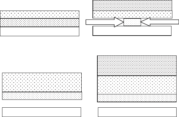
Sapphire
MBE ZnO
MBE GaN
(a) (b)
Sapphire
MBE GaN
HVPE GaN (900 ºC)
MBE GaN
HVPE GaN (1040 ºC)
ZnO
(c)
Sapphire
HVPE GaN (900 ºC)
MBE GaN
(d)
Sapphire
in-situ etching
HVPE GaN (900 ºC)
Figure 9.3 Schematic diagram of the growth sequence for free-standing GaN substrates. A
200 nm-thick single crystal ZnO layer with Zn polarity was first grownon c-plane sapphire using an
8 nm thick MgO bufferlayer depositedby plasma assisted molecular beam epitaxy followed by the
growth of a 1 mm-thick GaN layer (a). During the low temperature growth of a relatively thick (100
mm) GaN by HVPE, commencing at 700
o
C and ending at 900
o
C, the ZnO buffer was gradually
etched from the sides by NH
3
and HCl gases (b). The ZnO layer between sapphire and GaN layers
was completely etched offduringgrowth of low-temperature GaN buffer(c). This wasfollowed by
growth of the final high temperature GaN layer (d). Reprinted from S. W. Lee, et al., Strain-free
GaN thick films grown on single crystalline ZnO buffer layer with in situ lift-off technique, Appl.
Phys. Lett., 90, 061907. Copyright (2007) American Institute of Physics
Growth of GaN/ZnO 229
9.3 Compositional Analysis
Here we give one example of compositional analysis of ZnO films deposited by PLD.
Rutherford backscattering spectroscopy (RBS) analysis revealed that t he composition
of t he GaN films de posited at 600
C on ZnO is stoichiometric when liquid Ga target
was used in PLD growt h. A typica l RBS spectrum is shown in Figure 9.6. However,
films deposited by a solid GaN target at a lower substrate temperature of 850
Cwere
nonstoichiome tric because of insufficient N radicals during the growth of GaN, whereas
forhighersubstratetemperatures,stoichi ometric films were achieved.
[7,36]
Secondary
ion mass spectroscopy (SIMS) analysis showed that oxygen is one of the impurities in
the GaN layers and its concentration was much hi gher at the interfa ce. S i a nd C were
found throughout the entire depth of the samples and are most likely from the sapphire
substrates.
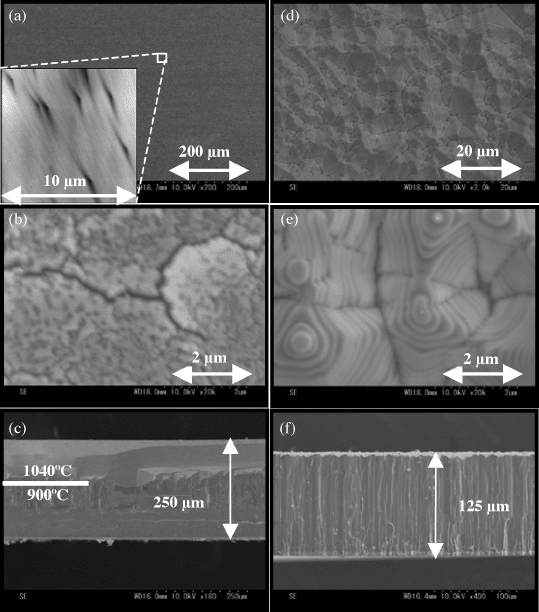
Figure 9.4 (a–c) SEM images of the free-standing GaN layers grown by the two-step growth
method by HVPE. (a) Top surface; (b) back-side surface; (c) side cut. (d–f) SEM images of the
free-standing GaN layers grown at 900
C. (d, e) Top surface; (f) side cut. (a, inset) AFM image
of a 10 10 mm
2
area with surface roughness of 1.44 nm. Reprinted from S. W. Lee, et al.,
Strain-free GaN thick films grown on single crystalline ZnO buffer layer with in situ lift-off
technique, Appl. Phys. Lett., 90, 061907. Copyright (2007) American Institute of Physics
230 Growth and Characterization
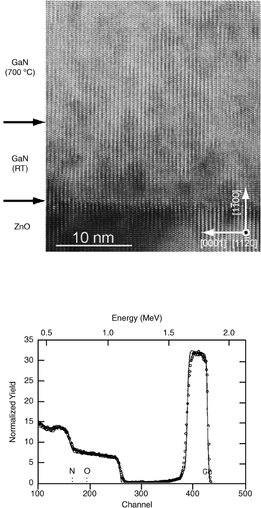
Figure 9.5 Cross-sectional TEM image of m-plane GaN (grown at 700
C)/GaN (grown at room
temperature)/m-ZnO substrate taken from the [
112
0]
direction. Reprinted from A. Kobayashi, et al.,
Room temperature epitaxial growth of m-plane GaN on lattice-matched ZnO substrates, Appl.
Phys. Lett., 90, 041908. Copyright (2007) with permissions from American Instituite of Physics
Figure 9.6 RBS spectrum of GaN thin films grown on ZnO/sapphire, He
2þ
beam energy is
2.3 MeV and the detector angle is 168
. The experimental curve is simulated with the
theoretical curve to attain the composition of the films. Reprinted from R. F. Xia, et al., Growth
of gallium nitride thin films by liquid-target pulsed laser deposition, J. Vac. Sci. Technol. A 15,
2207. Copyright (1997) with permission from American Vacuum Society
Compositional Analysis 231
9.4 Structural Analysis
Various characterization methods have been used to analyze the structural properties of
GaN and specific to the theme of this section, GaN on ZnO with a few examples on other
substrates such as fused silica. XRD analysis showed that the GaN films grown directly on
fused silica substrates are not only polycrystalline with different orientations, (1010) ,
(0002) and (1011) but also are characterized with low intensities of diffraction p eaks.
[8]
The XRD spectrum is dominated by the (0002) reflection when GaN films were deposited
at a substrate temperature (T
s
) of 600
C; its significance is low for films grown at higher or
lower temperatures. The FWHM of the rocking curve for the (0002) diffraction was 0.21,
0.20, and 0.52
o
for GaN/ZnO/Si (111), GaN/ZnO/sapphire (0001) and ZnO/sapphire,
respectively.
[36]
The FWHM of the (0002) reflection for ZnO films on sapphire was 0.17
for a substrate temperature of 750
C and O
2
pressure of 10
5
–10
4
Torr. The X-ray w scans
of ZnO films deposited at two deposition conditions, (a) T
s
¼500
C with a pulse repetition
rate of 15 Hz and (b) T
s
¼750
C with a pulse repetition rate of 10 Hz, were recorded. The
X-ray analysis showed that the substrate and the epitaxial layer are oriented with respect to
each other by a 30
rotation of the unit cells. The in plane epitaxial and substrate
relationship is ZnO[101
0]kAl
2
O
3
[112
0]. A similar fashion of orientation can be seen for
AlN and GaN on sapphire, as shown in Figure 9.7. The FWHM of the rocking curve of the
(0002) diffraction for GaN, AlN, ZnO growth on sapphire was less than 0.15
. The AlN
films were deposited on ZnO/sapphire at T
s
¼950
C with the same technique and its
FWHM is 0.23
.
[7]
The (0002) diffraction peaks are clearly resolved for the structure of
ZnO/GaN, showing high crystalline quality of the films, as shown in Figure 9.8.
Matsuoka et al.
[22]
observed that the etching rate of the O-face ZnO is faster than that of
the Zn-face by about one order of magnitude. The (0001) Zn-face ZnO on sapphire
substrates was used for the growth of In
0.22
Ga
0.78
N layers. The single crystal ZnO layers
were nitrided using ammonia at 76 Torr and 500
C for 10 min. In the nitrided substrates,
the RHEED showed a ring pattern, indicating that a polycrystalline film formed on the
surface of the ZnO substrate. The XRD analysis revealed only the (0002) reflection of both
ZnO and InGaN, and no other peaks could be observed (Figure 9.9). The RHEED pattern
was streaky for the films grown on ZnO indicating single crystal nature whereas films
deposited on sapphire were polycrystalline. The rough and smooth mirror-like surfaces
were observed for InGaN films grown on ZnO and sapphire, respectively. The XRD line
width of InGaN grown on ZnO is about 20% smaller than that of films grown on sapphire
substrates. It is clear that the remarkable improvement in the crystalline quality of the films
has been achieved. Ueda et al.
[12]
found that if pulsed laser deposited ZnO layer thickness
is up to 50 nm, the FWHM for GaN grown on it is smaller by a factor of two than that of
thicker ZnO films. However, for a 200 nm-thick ZnO buffer layer, the rocking curve was
broader due to segregation of crac ks in the subsequent GaN layer.
Wang et al.
[10]
reported that the FWHM of rocking curve of the (0002) diffraction for
GaN/ZnO is 0.38
, which was wider, if ZnO buffer layer had not been used. The FWHM
decreased from 0.45 to 0.22
with increasing ambient pressure from 10
5
to 1 Torr for GaN
films grown on ZnO, as shown in Figure 9.10(a). Similarly, this value decreased with
increasing substrate temperature, as shown in Figure 9.10(b). The GaN films deposited at
H500, 700, and 800
C under 0.1 Torr in N
2
ambient showed amorphous, polycrystalline,
232 Growth and Characterization