Litton C.W., . Reynolds D.C., Collins T.C. Zinc Oxide Materials for Electronic and Optoelectronic Device Applications
Подождите немного. Документ загружается.


peak was observed at 3.3206 eV with LO phonon replicas at 3.2505 eV and 3.180 eV,
which is attributed to donor-acceptor transition.
[43]
As for the defect-related features, only
the broad band with the maximum at about 2.4 eV (green band) is resolved. The low-
temperature PL spectrum of the Cermet sample is nearly identical to that of the Hanscom
sample. However, the FWHM of the 3.36 eV peak is lower approximately by a factor of
three than that of the Hanscom sample. The broad defect related band was observed at
about 2.1 eV instead of the green band. In the Eagle Piche r sample, the PL spectra from
two faces (Zn and O) were compared at room temperature, in an effort to identify the
transitions. Now it is easy to analyze PL spectra of GaN deposited on ZnO, if any traces of
ZnO or mixed phase of GaN and ZnO appeared. The low-temperature PL spectru m of GaN
grown on ZnO compared with GaN grown on other substra tes is shown in Figure 9.22. The
FWHM of the excitonic peak was found to be about 13 meV for GaN/ZnO and a sharp
Figure 9.20 CL spectra of sample 4 (n
s
¼5 10
16
cm
2
) at different interface distances.
Reprinted from X. L. Sun, et al., Depth-dependent investigation of defects and impurity doping
in GaN/sapphire using scanning electron microscopy and cathodoluminescence spectroscopy.
J. Appl. Phys., 91, 6729. Copyright (2002) with permission from American Institute of Physics
Optical Properties 243
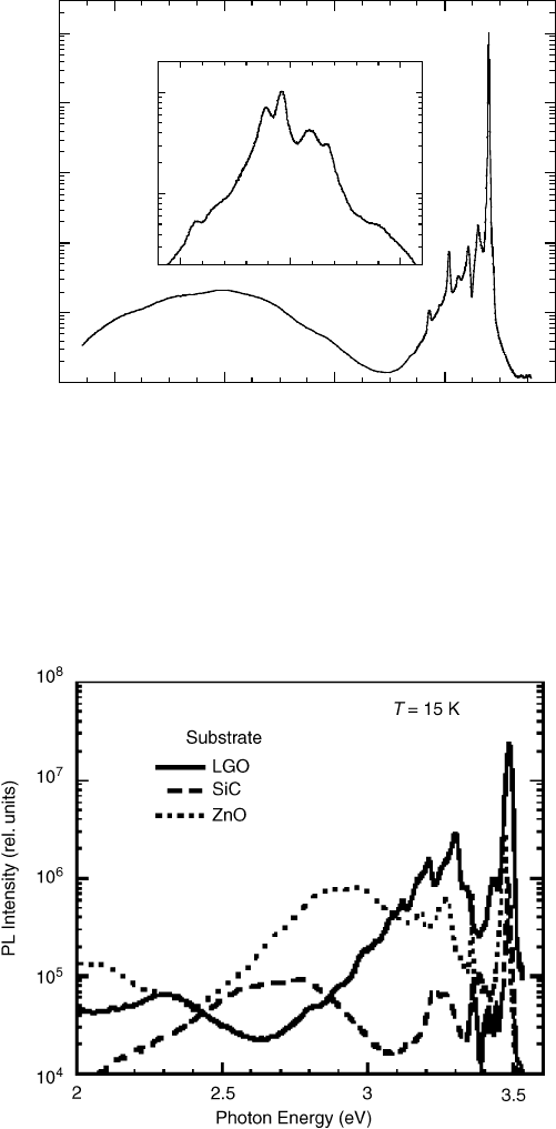
peak at 3.358 eV is due to excitonic emiss ion from the underlying ZnO substrate in
PL spectra. Gu et al. reported that the high radiative efficiency and weaker yellow
luminescence was obser ved in GaN/ZnO, as compared with other substrates.
[18]
The exciton peak of GaN/ZnO was very slightly blue-shifted while that for GaN/SiC
10
0
10
1
10
2
10
3
10
4
10
5
3.63.22.82.42
PL Intensity (a.u.)
Photon Ener
g
y (eV)
T = 10 K
Bulk ZnO
3.3653.363.355
Figure 9.21 PL spectra of ZnO substrate (produced by Cermet Inc.) at 10 K. Theinset shows
the enlarged fine structure in the near-band-edge region
Figure 9.22 Low temperature PL spectra of GaN grown without buffer on different substrates.
Reprinted from F. Yun, et al., Mat. Res. Soc. Symp. Proc., 719, F8.21. Copyright (2002) with
permission from MRS
244 Growth and Characterization
is red-shifted. It is a clear indication that the blue and red shifts are due to compressive and
tensile strains of GaN/ZnO and GaN/SiC, respectively.
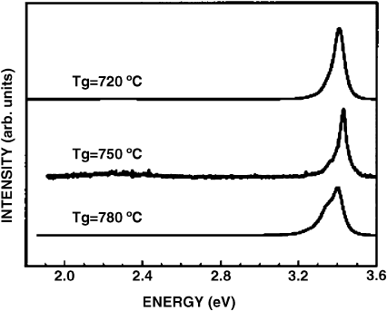
Hamdani et al.
[21]
demonstrated that the growth temperature is one of the important
factors while depositing GaN on ZnO by using NH
3
in the MBE system. Room
temperature PL spectra of GaN grown on the O-face ZnO subst rates at different
temperatures, i.e. 720, 750, and 780
C, are shown in Figure 9.23. At room temperature
the FWHM of the band edge emission increased from 36 to 60 meV with increasing
growth temperature from 720 to 780
C, respectively, due to increasing etching rate by
NH
3
on the substrates with effect of temperature. The FWH M was found to be 8 meV at
4.2 K for the films grown at 720
C. Moreover, any GaN growth was not observed at higher
growth temperatures such as 800
C. At low temper ature, the intensity ratio of the free
exciton peak and the donor bound exciton of GaN films grown on the O-fac e ZnO is two
orders of magnitude higher than that of films on the Zn-face ZnO substrates. However, Gu
et al. also achieved good quality GaN layers on Zn-face ZnO substrates.
[18]
Figure 9.24 shows the low temperature PL and reflectivity spectra of the films grown on
O-face ZnO substra tes at growth temperature of 750
C. A, B and C excitons at 3.476,
3.489 and 3.511 eV, respectively, and interference fringes due to multiple reflections of
emission beam between the surface of GaN and GaN/ZnO interface are seen in the
reflectivity spectrum. In the PL spectrum, the main peaks were attributed to free A exciton,
a bound exciton and DAP.
[21,44]
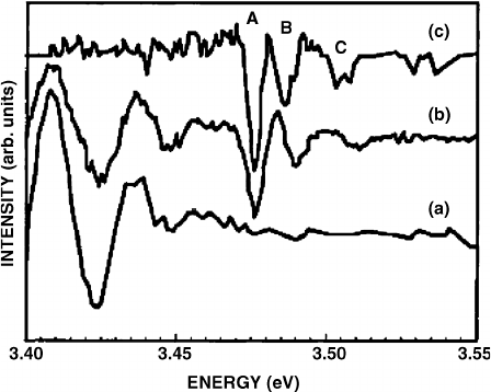
Similarly, the PL and reflectivity spectra were recorded for
GaN films grown on the Zn-face of ZnO substrates,
[21]
as shown in Figure 9.25. A and B
excitons only pronou nced at 3.481 and 3.496 eV, respectively, and the broadening of free
exciton (A) in the reflectivity spectrum reflects the lower crystalline quality of the GaN
films. Moreover, the donor bound exciton, DX, with a binding energy of 12 meV occurred
instead of the free A exciton peak in the PL spectrum when comparing with Figure 9.24.
Figure 9.23 Room temperature PL spectra of GaN grown without buffer on O-face ZnO at
different growth temperatures. Reprinted from F. Hamdani, A. E. Botchkarev, H. Tang, W. Kim,
and H. Morkoc¸ , Effect of buffer layer and substrate surface polarity on the growth by molecular
beam epitaxy of GaN on ZnO, Appl. Phys. Lett. 71, 3111. Copyright (1997) with permission
from American Institute of Physics
Optical Properties 245
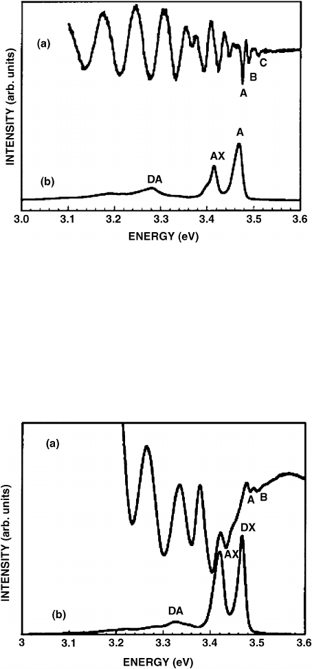
Figure 9.24 Low temperature (a) differential reflectivity and (b) PL spectra of GaN grown
without buffer on O-face ZnO. A, B and C, free excitons; AX, bound exciton; and DA,
donor–acceptor pair. Reprinted from F. Hamdani, A. E. Botchkarev, H. Tang, W. Kim, and H.
Morkoc¸, Effect of buffer layer and substrate surface polarity on the growth by molecular beam
epitaxy of GaN on ZnO, Appl. Phys. Lett. 71, 3111. Copyright (1997) with permission from
American Institute of Physics
Figure 9.25 Low temperature (a) differential reflectivity and (b) PL spectra of GaN grown
without buffer on Zn-face ZnO. DX, bound exciton. Reprinted from F. Hamdani, A. E.
Botchkarev, H. Tang, W. Kim, and H. Morkoc¸ , Effect of buffer layer and substrate surface
polarity on the growth by molecular beam epitaxy of GaN on ZnO, Appl. Phys. Lett. 71, 3111.
Copyright (1997) with permission from American Institute of Physics
246 Growth and Characterization
An additional shift of the free exciton peak on about 5 meV indicates that the GaN films
grown on the Zn-face ZnO substrates are under more compressive stress than the films on
the O-face ZnO due to the difference in interface bonding between ZnO and GaN. The
reflectivity derivative spectra of the GaN grown on the O-face ZnO with different buffer
layers such as GaN, AlN and In
0.20
Ga
0.80
N are given in Figure 9.26. A, B and C excitons
clearly appeared and shifted to lower photon energies for GaN/ZnO with the In
0.20
Ga
0.80
N
buffer layer whereas in other cases no red shift was observed. This might be due to the
strain relaxation between the In
0.20
Ga
0.80
N buffer layer and GaN.
[21]
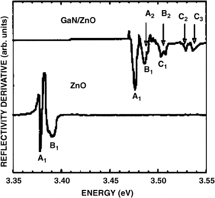
Figure 9.27 shows the
reflectivity derivative spectra of ZnO and GaN/ZnO in which the ground and excited levels
of free excitons labeled A
1
,A
2
,B
1
,B
2
, etc., occurred for GaN/ZnO, when In
0.20
Ga
0.80
N
was used as a buffer layer indicating better quality of the GaN epilayers.
[21]
Hamdani et al.
[16]
found from PL spectra that the FWHM of the room temperature band
edge emission was 80 and 36 meV for GaN/ZnO and ZnO substrate, respectively, and the
observation of free exciton in the low-temperature PL spectrum is confirmation of the high
quality of both materials. The intensity ratio of the free and bound excitons is higher for GaN/
ZnO compared with ZnO in the low-temperature PL spectra, and thus it can be concluded that
the quality of the epitaxial layers is higher, when ZnO is used as the substrates. The positions
of A, B, C excitons in GaN grown on a ZnO substrate obtained from the reflectivity spectra
slightly blue-shifted compared with the positions in bulk GaN. It indicates small compressive
strain between these layers. However, the excitonic positions, in the case of InGaN buffer
which is closely lattice matched to the GaN, shifted to lower energy levels compared with the
positions of GaN grown directly on ZnO. On the other hand, the yellow luminescence did not
appear at low temperatures, further proving the high quality of the samples, though at very
low excitation levels it has been observable. The excitonic peaks were not observed in GaN
Figure 9.26 Reflectivity derivative spectra of GaN grown on O-face ZnO with different buffer
layers: (a) AlN; (b) GaN; and (c) In
0.20
Ga
0.80
N. The growth temperature of the buffer layers was
650
C.ReprintedfromF.Hamdani,A.E.Botchkarev,H.Tang,W.Kim,andH.Morkoc¸, Effect of
buffer layer and substrate surface polarity on the growth by molecular beam epitaxy of GaN on ZnO,
Appl. Phys. Lett. 71, 3111. Copyright (1997) with permission from American Institute of Physics
Optical Properties 247
grown on AlN buffer layers.
[21]
In PL spectra, A (3.375 eV), B (3.386 eV) free exciton and
D
0
X (3.364 eV) peaks were seen in GaN/ZnO whereas A, B and A2 exciton peaks with
binding energy of 67 meVappeared in ZnO substrate.
[44]
The segregation of free exciton is a
sign of low carrier concentration and high crystalline quality of the ZnO substrate. The
properties of the grown GaN layers depend not only on the type of the buffer or substrate used
for the growth but also on the polarity of the buffer or substrate. One can see the segregation of
different peaks from GaN, if the Zn-face or the O-face ZnO substrates were used,
[16]
as shown
in Figure 9.28.
In the PL spectra at 77 K from GaN grown on sapphire substrate with ZnO buffer layer,
the BL band is seen.
[12]
Note that the band edge emission peak at 3.45 eV segregated in
both type s of samples with and without buffer layers. However, in the ZnO/GaN layers,
a wide peak at 2.8 eV is due to the diffusion of Zn into GaN. Detchprohm et al.
[13]
studied
the low temperature PL properties of GaN films grown on sput ter deposit ed Zn O at
different ambients such as Ar and O
2
. The peaks at 3.486 and 3.479 eV are due to free and
donor bound excitons, respectively, observed in both GaN samples. However, the FWHM
(2.58 meV) of PL peak due to exciton bound to neutral donor for GaN grown in Ar is less
than that of the GaN grown in O
2
. It was concluded that the films grown using ZnO buffer
showed high crystalline quality. The donor bound excitons and free excitons are observed
in the PL spectra of GaN grown on sapphire with ZnO buffer layer. The very weak yellow
luminescence at 2.2 eV was also present.
[14]
In the Raman spectra, the coupled plasmon-phonon mode, in addition to two E
2
modes
at 570 and 143 cm
1
, was a broad line at approximately 510–530 cm
1
.
[12]
The broad nature
of this mode indicates that GaN films might have a higher carrier concentration. The
Figure 9.27 Reflectivity derivative spectra of ZnO substrate and GaN grown on ZnO with
thickness of 2 mm with InGaN buffer layer. Reprinted from F. Hamdani, et al., Microstructure
and optical properties of epitaxial GaN on ZnO (0001) grown by reactive molecular beam
epitaxy, J. Appl. Phys., 83, 983. Copyright (1998) with permission from American Institute of
Physics
248 Growth and Characterization
measured carrier concentration is in the order of 10
19
cm
3
. Regarding the surface, terrace-
like flat features were observed when growing GaN films on ZnO buffers.
[12]
9.7 Electrical Properties
Perhaps the most sensitive characterization method, one which also bodes well for
electronic devices, is electrical characterization, such as Hall measurements. In this
vein, Detchprohm et al.
[13]
found that the growth of GaN on sputtered ZnO in O
2
is
better than that of sputtered ZnO in Ar. The measured room temperature Hall mobility is in
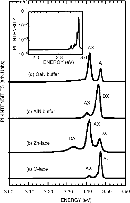
Figure 9.28 PL spectra of GaN grown on (a) O-face ZnO, (b) Zn-face ZnO, (c) with AlN buffer
on O-face ZnO and (d) with GaN buffer on O-face ZnO. A
1
, free exciton; DX, donor bound
exciton; and AX, acceptor boundexciton. The inset shows the spectrum over a wider energy range
including red and green wavelengths. Reprinted from F. Hamdani, et al., Microstructure and
optical properties of epitaxial GaN on ZnO (0001) grown by reactive molecular beam epitaxy, J.
Appl. Phys., 83, 983. Copyright (1998) with permission from American Institute of Physics
Electrical Properties 249
the range of 420–520 cm
2
V
1
s
1
for GaN films grown directly on sapphire. At room
temperature, the carrier concentration of 9 10
15
–410
16
cm
3
for GaN films grown on
ZnO is two or three orders of magnitude lower than that of the films grown on sapphire. A
relatively lower mobility value of 60 cm
2
V
1
s
1
and a higher carrier conce ntration of
6 10
19
cm
3
for GaN films grown on ZnO by PLD are reported in the literature.
[7]
The
carrier concentration and mobility of In
0.23
Ga
0.77
N films grown on ZnO substrates at
800
C are 1 10
18
cm
3
and 100 cm
2
V
1
s
1
, respectively.
[22]
The electron concentration
and the Hall mobility are 7 10
16
cm
3
and 880 cm
2
V
1
s
1
at 293 K and 4 10
16
cm
3
and
2248 cm
2
V
1
s
1
at 120 K for 74 mm-thick ZnO pretreated GaN sample. A little variation in
electrical properties was noted for over 2 inch sample, showing homogeneity of the sample
grown by Molnar et al.
[14]
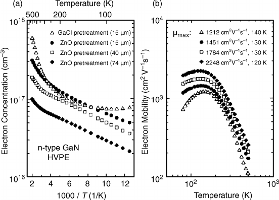
Electrical measurements, which were carried out on
n-GaN grown by HVPE and treated by either GaCl, or ZnO, effectively showed thickness
dependence. As depicted in Figure 9.29, the Hall mobility increased with increasing
thickness of the GaN film/ZnO/sapphire. This is a clear indication that the defect
concentration decreased with increasing thickness of the film ranging from 4.5 to 74 mm.
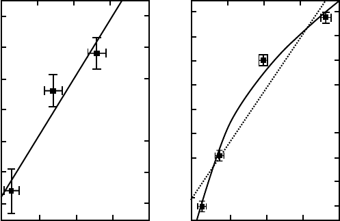
A two-layer model was proposed by Look and Molnar,
[45]
and extended by G
€
otz et al.,
[46]
to obtain more accurately the bulk mobility and electron concentration when a highly
conductive interfacial layer is inserted. The effective areal density of free electrons n
s,eff
and the effective Hall mobility m
eff
are related to the free electron concentration n(x) and
electron mobility m (x):
n
s;eff
ðdÞ¼
ð
d
0
nðxÞmðxÞdx
#
2
,
ð
d
0
nðxÞmðxÞ
2
dx
2
4
ð9:1Þ
Figure 9.29 (a) Variation of electron concentration vs inverse temperature and (b) electron
mobility vs temperature for GaN layers grown by HVPE. Reprinted from R. J. Molnar, W. G
€
otz,
L. T. Romano, N. M. Johnson, Growth of gallium nitride by hydride vapor-phase epitaxy, J.
Cryst. Growth, 178, 147. Copyright (1997) with permission from Elsevier
250 Growth and Characterization
and
m
eff
ðdÞ¼
ð
d
0
nðxÞmðxÞ
2
dx=
ð
d
0
nðxÞmðxÞdx ð9:2Þ
The final product can be derived from Equations (9.1) and (9.2):
n
s;eff
m
eff
ðdÞ¼
ð
d
0
nðxÞmðxÞdx ð9:3Þ
For layer 1: 0 G x d
1
, n(x) ¼n
1
, m(x) ¼m
1
and for layer 2: d
1
G x d
1
þd
2
¼d,
n(x) ¼n
2
, m(x) ¼m
2
.
Equation (9.3) becomes (d
1
d
2
d)
n
s;eff
m
eff
ðdÞn
1
m
1
d
1
þn
2
m
2
d
2
ð9:4Þ
Equation (9.4) predicts a linear dependence of n
s,eff
m
eff
on film thickness (d). Experi-
mentally, linearity was observed for the product of n
s,eff
m
eff
vs thickness for GaCl-treated
samples, whereas for the ZnO-treated samples, a slightly nonlinear behavior was observed,
as shown in Figure 9.30. One could believe that there might be some disturbance at the
interface, for which some arbitrar y decay parameters are introduced in the equations:
nðxÞ¼n
1
expðx=d
n
Þþn
2
ð9:5Þ
(a)
14
12
10
8
6
4
2
45
40
35
30
25
20
15
10
5
HVPE GaN
GaCI pretreatment
T=300 K
HVPE GaN
ZnO pretreatment
T=300 K
0510
15 20
020 406080
Thickness (µm) Thickness (µm)
n
seff
µ
eff
(10
16
cm
–2 +
cm
2
V
–1
s
–1
)
n
seff
µ
eff
(10
18
cm
–2 +
cm
2
V
–1
s
–1
)
(b)
Figure 9.30 Product of electron density (n
s,eff
) and mobility (m
eff
) vs thickness of GaN layer for
(a) GaCl-treated samples and (b) ZnO-treated samples. The solid and dotted lines are the linear
fit to the experimental data. Reprinted from W. G
€
otz, L. T. Romano, J. Walker, N. M. Johnson,
and R. J. Molnar, Hall-effect analysis of GaN films grown by hydride vapor phase epitaxy, Appl.
Phys. Lett., 72, 1214. Copyright (1998) with permission from American Institute of Physics
Electrical Properties 251
mðxÞ¼m
2
m
1
expðx=d
m
Þð9:6Þ
where n
2
and m
2
represent the electron concentration and mobility for a thick GaN film,
respectively, and n
1
þn
2
and m
2
m
1
are roughly related to electron conce ntration and
mobility near the GaN/sapphire interface, respectively. The terms d
n
and d
m
represent the
increase and decrease of the electron concentration and mobility, respectively. From
Equations (9.1), (9.2), (9.5) and (9.6):
n
s;eff
ðdÞ¼AðdÞ
2
=BðdÞ and m
eff
ðdÞ¼BðdÞ=AðdÞð9:7Þ
where
AðdÞ¼n
1
m
1
d þn
1
m
2
d
m
½expðd=d
m
Þ1n
2
m
1
d
n
½expðd=d
m
Þ1
and
BðdÞ¼n
1
m
1
2
d1 = 2n
1
m
2
2
d
m
½expð2d=d
m
Þ1þ2n
1
m
1
m
2
d
m
½expðd=d
m
Þ1
n
2
m
2
1
d
n
½expðd=d
n
Þ1
ð9:8Þ
The theoretically determined electron concentration a nd mobility are: n
2
¼3.5
10
16
cm
3
and m
2
¼903 cm
2
V
1
s
1
for a thick film; and n
1
þn
2
¼4.3 10
17
cm
3
and
m
2
m
1
¼216 cm
2
V
1
s
1
for t he interface between sap phire and GaN. The reporte d
highest mobility value of GaN grown on sapphire with ZnO buffer is 2248 cm
2
V
1
s
1
at 120 K.
[14]
TEM analysis revealed that there is no interface between sapphire and
GaN when ZnO is used as a buffer. These results solely support the electrical analysis.
9.8 GaN/ZnO Hybrid Devices
Because p-type ZnO had been relatively hard to attain, hybrid het erostructures in which
the p-type material was of some other semiconductor have been explored. Furthermore,
for some device features integration of GaN and ZnO technologies paves the way for
enhanced performance and/or make certain device functions possible. To reiterate,
semiconductor ZnO has a direct band gap of 3.3 eV with a wurtzite structure. In many
respects ZnO competes wit h GaN for device applications. It is also clear that GaN h as
been shown to be capable of producing very high performance electronic and optical
devices. Issues such as reliability, efficiency, etc., are being explored which is indicative
of a success story. Power field effect transistors are capable of producing over 500 W of
CW power in the communication band, LEDs have become very popular with current
emphasis on efficiency while they are already more efficient than fluorescent bulbs, and
blue lasers are already used in the Sony Play Station III for high definition viewing. The
same, however, cannot necessarily be said about ZnO at this point. As already
mentioned, the applications of ZnO overlap a good deal with those of GaN. On the
electronic side, the relatively low mobilit y of ZnO compared with GaN and stronger
electron–phonon coupling together with relatively low thermal conductivity are serious
shortcomings for ZnO. However, transparent thin film transistors built in poly-ZnO
252 Growth and Characterization