Litton C.W., . Reynolds D.C., Collins T.C. Zinc Oxide Materials for Electronic and Optoelectronic Device Applications
Подождите немного. Документ загружается.

appear to hold some potential, and so do the already established surface acoustic
wave devices.
It still remains to be seen, however, as to how competitive ZnO would be with existing
technologies. On the optical device front, ZnO needs to show high p-type conductivity
along with heterojunctions for competitive devices to be built. Again the competition is
GaN, which is well on its way to dominating the optical device development arena in the
short wavelength end of the visible spectrum and UV. One advantage that ZnO has over
GaN is the 60 meV exciton binding energy, compared with 25 meV for GaN. In addition,
ZnO appears to be a more efficient light emitter compared with GaN. If lasers utilizing
excitonic transitions were to be built, ZnO would have an advantage over GaN provided
that p-type conductivity is obtained and other necessary processing capab ilities are
developed for ZnO. Further, electromechanical coupling of ZnO, particularly along the
c-direction is higher than that of GaN, which could pave the way for applications such as
surface acoustic wave devices. Further yet, if and when the highly hyped and touted
nanostructures were to be of use, ZnO appears to be better suited for producing those
structures. The worldwide shortage of In at a time of expanding demand for ITO seems
to be opening the door for ZnO-based transparent oxides, i.e. AlZnO (or AZO for short), to
be explored. If successful, this application area is huge.
In this section, we focus our attention on GaN/ZnO hybrid devices. As already
mentioned, ZnO buffer layers and ZnO substrates have the potential to improve the
quality of GaN-based emitters. ZnO itself is also a very promising material for UV-visible
light emission. Hereafter, we review the recent progress on hybrid ZnO/GaN heterojunc-
tion LEDs and some other hybrid optical devices.
9.8.1 Hybrid ZnO/GaN Hetero junction LED
Alternative approaches which are based on hybrid heterojunctions combining p-doped
GaN and n-doped ZnO have been realized. Alivov et al.demonstratedroom temperature
electroluminescence (EL) from n-ZnO:Ga/p-GaN:Mg (grown by MBE)/c-sapphire
[47]
and n-ZnO:Ga (grown by MOCVD)/p-AlGaN:Mg (grown by HVPE)/GaN (grown by
HVPE)/6H-SiC
[48]
heterojunction LEDs, having emission wavelengths of 430 nm and
389 nm, respectively. In the form er case, diode-lik e current–voltage (I–V) characteristics
were observed under forward bias. The latter provided much better I–V char ac teri sti cs
with threshold voltage 3.2 V as shown in Figure 9.31 and low reverse leakage current
10
7
A at room temperature. This UVemission at 389 nm at room temperature when the
diode is forward biased and operated up to 500 K was attributed to the radiative
recombination in ZnO.
To improve optical and thermal characteristics of LEDs, UV LEDs based on p-n
junction n-Zn
0.9
Mg
0.1
O/n-ZnO/p-Al
0.16
Ga
0.84
N/p-GaN triple heterostructures were grown
by RF plasma-assisted MBE.
[49,50]
The charge distribution and band diagram of this
structure are shown in Figure 9.32. The free carrier concentration in MgZnO and ZnO was
assumed to be 3 10
17
cm
3
, with free hole concentrations in AlGaN and GaN assumed
to be 1 10
17
and 3 10
17
cm
3
, respectively. The measured I–V characteristics shown in
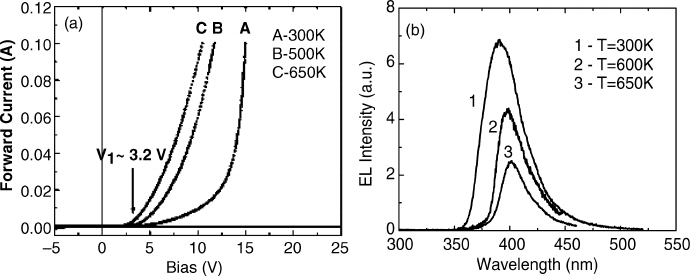
Figure 9.33(a) have rectifying characteristics with a turn-on voltage of 3.2 V. Strong UV
emission at 390 nm assumed to originate from excitonic transition in ZnO was observed
up to 650 K [Figure 9.33(b)].
GaN/ZnO Hybrid Devices 253
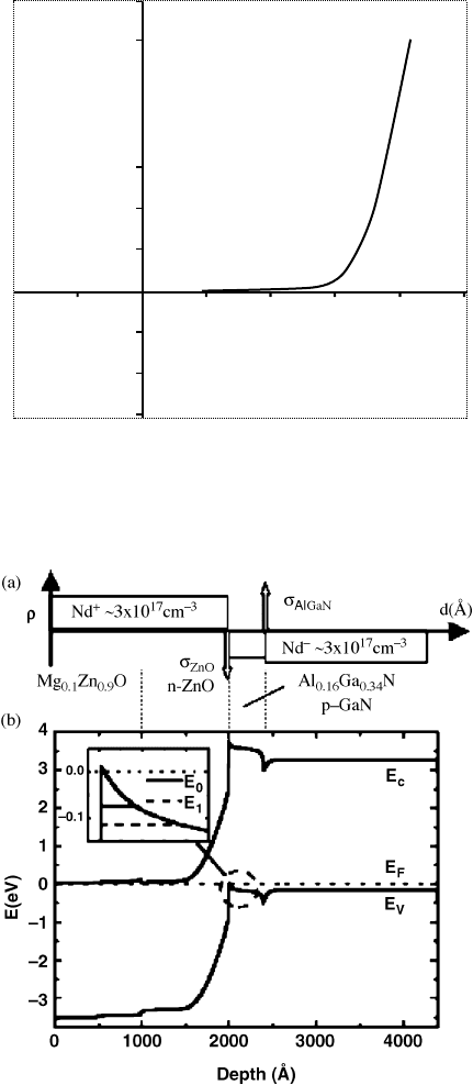
Figure 9.32 (a) Charge distribution and (b) band diagram of the p-n junction MgZnO/ZnO/
AlGaN/GaN heterostructure. The layer thicknesses are 100, 100, 40 and 200 nm, respectively.
Reprinted from A. Osinsky, J. W. Dong, M. Z. Kauser, B. Hertog, A. M. Dabiran, P. P. Chow, S. J.
Pearton, O. Lopatiuk, and L. Chernyak, MgZnO/AlGaN heterostructure light-emitting diodes,
Appl. Phys. Lett., 85, 4272. Copyright (2004) with permission from American Institute of Physics
70
60
50
40
30
20
10
0
–10
–20
–30
–2 –1 0 2 3 4 5
Current (mA)
Bias voltage (V)
Figure 9.31 Room temperature I–V characteristics of the n-ZnO/p-Al
0.12
Ga
0.88
N structure.
Reprinted from Y. I. Alivov, et al., Fabrication and characterization of n-ZnO/p-AlGaN
heterojunction light-emitting diodes on 6H-SiC substrates, Appl. Phys. Lett., 83, 4719.
Copyright (2003) with permission from American Institute of Physics
254 Growth and Characterization
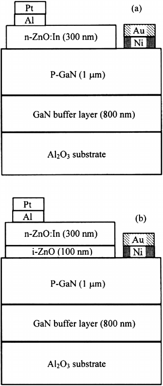
p-GaN/n-ZnO:In (p-n) and p-GaN/i-ZnO/n-ZnO:In (p-i-n) heterojunction LEDs were
fabricated by the vapor cooling condensation system,
[51]
in which the material sources were
put on a tungsten boat and heated. Then the sublimated material vapor gases were allowed to
condense and deposit onto the substrate cooled by liquid nitrogen.The electron concentration
and mobility of the deposited n-ZnO:In were 1.7 10
20
cm
3
and 3.7 cm
2
V
1
s
1
, respec-
tively, and for i-ZnO were 7.6 10
15
cm
3
and 2.17 cm
2
V
1
s
1
. For the PL spectra, near-
band-edge emission of 380 nm and broad band emission due to what was assumed to be the
oxygen vacancies of 540 nm for n-ZnO:In and near-band-edge emission of 382 nm having
FWHM of 13 nm for i-ZnO were observed. Figure 9.34 shows the schematic diagrams of the
p-n and p-i-n heterojunction LED structures. As shown in Figure 9.35, the room temperature
I–V characteristics of these LED structures show rectifying diode-like behavior. For the p-n
heterojunction LEDs, the forward turn-on voltage and reverse breakdown voltage were 3 and
15 V, respectively, compared with 7 and 23 V for the p-i-n heterojunction LEDs. In the
room temperature EL spectrum, the p-n heterojunction LEDs have a broad emission band at
432 nm, which is attributed to the transition from the conduction band to the acceptor
level ascribed to the Mg-doped p-GaN when electrons are injected from the n-ZnO:In into the
Mg-doped p-GaN. The EL emission peak of p-i-n heterojunction LEDs is at 385 nm, which
corresponds to the PL emission wavelength of the i-ZnO.
High brightness UV-blue-green InGaN-based quantum well (QW) LEDs are now
commercially available. However, the performance of InGaN-based green LEDs is still
far from sufficient for use in solid-state lighting. This is because higher In composition and
thick well width are needed to obtain the green emission and the internal field becomes
large when the In composition and well width increases. InGaN with high In composition
becomes unstable at high temperatures, which is required for high quality n-doped GaN
growth. To overcome these challenges, hybrid n-ZnO/(InGaN/GaN) multi-quantum wells
(MQWs)/p-GaN LEDs were achieved by Bayram et al.
[52]
The reason why n-ZnO layer by
PLD is used is that ZnO layer can be grown at lower temperatures as compared with
conventional MO CVD growth to protect the QWs. Note that the refractive index of ZnO at
Figure 9.33 (a) Forward bias I–V characteristics of triple heterostructure UV LED measured at
different temperatures. Curves A, B, and C correspond to measurements at 300, 500 and 650 K,
respectively. At 100 mA current, the series resistance is 150 W and is 105 W for 300–650 K.
Reprinted from H. S. Yang, et al., Fabrication of Hybrid n-ZnMgO/n-ZnO/p-AlGaN/p-GaN
Light-Emitting Diodes, Jpn. J. Appl. Phys., 44, 7296 Copyright (2005) with permission from the
Japan Society of Applied Physics
GaN/ZnO Hybrid Devices 255
500 nm is 2.0 compared with 2.5 for GaN. In this manner, lower critical angle loss can
be expected for light extraction through ZnO-capped LEDs. Hybrid n-ZnO/(InGaN/GaN)
MQWs/p-GaN LEDs were grown by MOVCD and PLD. The device structure is illustrated
in the inset of Figu re 9.36. p-GaN was grown on a 600 nm-thick AlN buffer layer on
sapphire by MOCVD. To activate the Mg dopant, thermal annealing was performed at
1000
C for 30 s. Hole carrier concentration of p-GaN was determined to be 7.8 10
17
Figure 9.34 The schematic diagrams of (a) p-GaN/n-ZnO:In and (b) p-GaN/i-ZnO/n-ZnO:In
heterojunction LED structures. Reprinted from R. W. Chuang, R. X. Wu, L. W. Lai, and C. T. Lee,
ZnO-on-GaN heterojunction light-emitting diode grown by vapor cooling condensation
technique, Appl. Phys. Lett., 91, 231113. Copyright (2007) with permission from American
Institute of Physics
256 Growth and Characterization
Figure 9.35 I–V characteristics at room temperature of p-n and p-i-n heterojunction LEDs.
Reprinted from R. W. Chuang, R. X. Wu, L. W. Lai, and C. T. Lee, ZnO-on-GaN heterojunction
light-emitting diode grown by vapor cooling condensation technique, Appl. Phys. Lett., 91,
231113. Copyright (2007) with permission from American Institute of Physics
Figure 9.36 (a) I–V curve of the fabricated LEDs. The device structure is illustrated in the inset.
(b) Leakage current vs reverse-bias voltage: experimental and theoretical fits for the reverse
voltage range from 1.6 to 5.4 V. Reprinted from C. Bayram, F. Hosseini Teherani, D. J.
Rogers, and M. Razeghi, A hybrid green light-emitting diode comprised of n-ZnO/(InGaN/
GaN) multi-quantum-wells/p-GaN, Appl. Phys. Lett., 93, 081111. Copyright (2008) with
permission from American Institute of Physics
GaN/ZnO Hybrid Devices 257
cm
3
by Hall effect measurements. Five periods of InGaN/GaN quantum wells were grown
in nitrogen ambient. Each period consisted of a 2 nm-thick InGaN quantum well with a
4 nm-thick GaN barrier. An n-ZnO layer was grown on top of the (InGaN/GaN) MQW/p-
GaN by PLD to complete the LED structure. A typical I–V curve for a hybrid green LED is
shown in Figure 9.36(a). The turn-on voltage was 2.5 V and the calculated on-series
resistance was 4.75 W. This high value is due to (1) high contact resistance because
the meal contacts to the p-GaN were not annealed and (2) the closeness (70 nm) of the
p-contact to the GaN/AlN interface. As shown in Figure 9.36(b), a nonlinear increase in
the leakage current with respect to the reverse-bias voltage was observed. The EL spectra
under pulsed injection (duty cycle of 10% and frequency of 5 kHz), as shown in
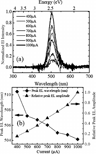
Figure 9.37, show linear dependence on the current densi ty. A blue shift from 510 to
504 nm was observed as the current increased from 400 to 1000 mA and the FWHM
decreased slightly from 194 to 179 meV. This is due to the band gap renormalization.
[53]
Figure 9.37 (a) Normalized EL intensity of the hybrid green LED at room temperature. (b)
Peak EL wavelength and amplitude with respect to injection current. Reprinted from C. Bayram,
F. Hosseini Teherani, D. J. Rogers, and M. Razeghi, A hybrid green light-emitting diode
comprised of n-ZnO/(InGaN/GaN) multi-quantum-wells/p-GaN, Appl. Phys. Lett., 93,
081111. Copyright (2008) with permission from American Institute of Physics
258 Growth and Characterization
9.8.2 ZnO-based Hybrid Mic rocavity
ZnO-based hybrid microcavities which consist of GaN-based distributed Bragg reflector
(DBR), ZnO-based cavity, and dielectric DBR are studied for a new type of coherent
optical source, namely polariton lasers. In the 1990s, the studies on semiconductor
microcavities paved the way to the development of cavity polariton technology.
[54]
Cavity
polaritons which are the elementary optical excitations in semiconductor microcavities
may be viewed as a superposition of excitons and cavity photons. The major feature of
cavity polariton technology centers on large and unique optical nonlinearities which would
lead to a new class of optical devices such as polariton lasers exhibiting very low threshold
and polariton parametric amplifiers with ultrafast response.
[55]
Among the wide-bandgap
semiconductors, GaN and ZnO are promising candidates for low threshold polariton
lasers operating at room temperature because of their large oscillator strengths and large
exciton binding energies, particularly ZnO with its unmatched exciton binding energy of
60 meV in bulk.
To reiterate, ZnO is a wide-bandgap semiconductor having a large exciton binding
energy (60 meV), much larger than that of GaN (23 meV), and a large oscillator strength,
and therefore, is a potential candidate like GaN for the realization of room temperature
polariton devices. The most adopted structure for the observation of polariton lasing is
a model ZnO-based microcavity proposed by Zamfirescu et al .
[56]
The structure consists of
a l-thick ZnO cavity layer sandwiched between ZnO/Zn
0.7
Mg
0.3
O DBRs having 14 and 15
pairs of l/4 thick layers on the top and at the bottom, respectively. Amazingly, the vacuum
Rabi split ting is as large as 120 meV in this model ZnO-based micro cavity, suggesting
room temperature polariton lasing to be possible. However, the ZnO technology is not so
well developed as yet as compared with that of GaN. Instead of all ZnO-based micro-
cavities, ZnO-based hybrid microcavities which consist of GaN-based DBR, ZnO-based
cavity layer and dielectric DBR were grown by MOCVD, plasma-assisted MBE and
plasma-enhanced CVD, respectively.
[57]
Figure 9.38 shows a cross-sectional image of a
ZnO-based hybrid microcavity which consists of a l -thick ZnO cavity layer sandwiched
between a 29 pair Al
0.5
Ga
0.5
N/GaN bottom DBR and an 8 pair SiO
2
/SiN
x
top DBR. The
bottom Al
0.5
Ga
0.5
N/GaN DBR was directly grown on a 200 nm-thick AlN buffer laye r on a
(0001) sapphire substrate by low-pressure MOCVD. The AlN buffer was chosen to
avoid cracking due to the built-in strain caused by lattice mismatch. The Al composition in
the AlGaN layer is nearly 50% as determined from XRD measurements, which also
revealed clear interference fringes indicative of smooth interfaces between layers. The
Al
0.5
Ga
0.5
N/GaN pair layer thickne ss was determined to be 77 nm from both XRD
measurements and cross-sectional SEM images.
A l -thick (optical thickness being 160 nm for l 380 nm in air) ZnO cavity layer was
grown on the bottom Al
0.5
Ga
0.5
N/GaN DBR by plasma-assisted MBE. The top dielectric
DBR which consisted of l/4-thick SiO
2
and SiN
x
layers was deposited on the ZnO half-
microcavity by ultra-high vacuum remote plasma-enhanced chemical vapor deposition
(UHV-RPECVD) to complete the microcavity structure. Angle-resolved measurements
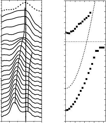
are conventional means to trace the cavity pola riton modes in microcavities without
changing the position or the temperature. By using the abovementioned ZnO microcavity
samples, the angle-resolved PL spectra were measured at room temperature over the range
0–40
using 325 nm excitation light from a He-Cd laser. The results are shown in
GaN/ZnO Hybrid Devices 259
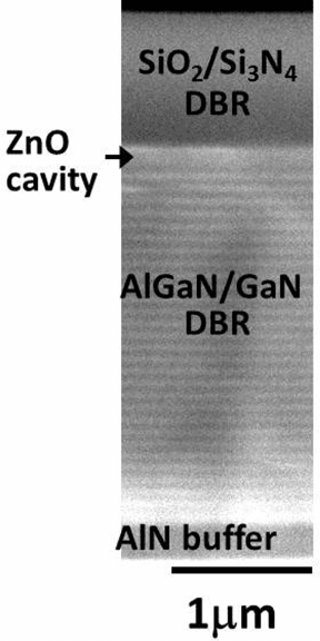
Figure 9.39(a), where the dotted line indicates the uncoupled exciton mode while the solid
lines are guides to the eye. As the angle increases, the lower polariton mode approaches the
uncoupled exciton mode, while the upper polariton mode is dispersed from the exciton
mode toward the cavity mode. These mode positions are plotted as a function of angle in
Figure 9.39(b), indicating a typical anticrossing behavior between the cavity mode and
exciton mode when the cavity mode crosses the exciton. Since the stopband width of the
bottom DBR is narrow (150 meV) due to relatively low refractive index contrast in
semiconductor DBR layers, the upper polariton features are not clear at large angles,
making it difficult to observe a clear anticrossing behavior. In addition, the relaxation
processes at the lower polariton branch and thermalization issues due to the large vacuum
Rabi splitting might be also responsible for poor resolution of the upper polariton branch.
Yet, the anticrossing behavior is clearly seen in Figure 9.39(b) and confirms the strong
coupling regime in ZnO-based hybrid microcavities. At the resonant condition of u ¼22
,
the vacuum Rabi splitting is estimated to be 50 meV. This value is far below the 120 meV
predicted by Zamfirescu et al.
[56]
The reason for such a large discrepancy is not clear
at present but might be partly attributed to the experimental problems such as the
Figure 9.38 Cross-sectional SEM image of a ZnO-based hybrid microcavity. Reprinted from
R. Shimada, J. Xie, V. Avrutin, U
¨
.O
¨
zgu
¨
r, and H. Morkoc¸ , Cavity polaritons in ZnO-based hybrid
microcavities, Appl. Phys. Lett., 92, 011127. Copyright (2008) with permission from American
Institute of Physics
260 Growth and Characterization
inhomogeneous broadening in the ZnO cavity layer and the low Q-value in the micro-
cavity. Polariton lasing depend s on the formation of a Bose–Einstein condensation at the
lower energy trap states in the lower polariton branch. High reso lution spectroscopy of
the lower polariton branch is imperative for the development of the polariton laser in the
strong coupling regime.
9.9 Conclusions
In summary, we have reviewed the growth and characterization of GaN on ZnO substrates
and on sapphire with ZnO buffer layer and related ZnO-based hybrid devices. The
structural analysis revealed that GaN grown on ZnO showed good quality crystallinity.
The reported CL measurements have given a clear picture about the quality of the layers
and the effect of the interface between ZnO and GaN. In PL studies, the observation of A
and B free exciton peaks bodes well for the quality of the GaN films grown on ZnO. By
using a two-layer model, the exact concentration and mobility of the films can be obtained.
Finally, ZnO-buffered GaN layers give us fruitful results rather than using just sapphire
substrates for the growth of GaN by HVPE. Moreover, for high performance and reliable
40
o
Photon energy (eV)
0
o
300K
403020100
3.22
3.23
3.24
3.25
3.26
3.27
3.28
3.29
3.30
3.31
3.32
3.33
An
g
le (de
g
.)
300K
3.43.33.2
0
o
(a)
PL intensity (arb. units)
0
o
Photon energy (eV)
(b)
Figure 9.39 (a) Angle-resolved PL spectra at room temperature in the range of 0 – 40
for a
l-thick ZnO hybrid microcavity. The dotted line is the exciton mode and the solid lines are
guides to the eye. (b) Experimental dispersion curves for upper and lower cavity polariton
modes. The dotted curves represent the uncoupled cavity and excition modes. Reprinted from
R. Shimada, J. Xie, V. Avrutin, U
¨
.O
¨
zgu
¨
r, and H. Morkoc¸, Cavity polaritons in ZnO-based hybrid
microcavities, Appl. Phys. Lett., 92, 011127. Copyright (2008) with permission from American
Institute of Physics
Conclusions 261
GaN-based devices, ZnO buffer layer and ZnO substrates also play a major role in
fabrication of free-standing GaN substrates and in the nonpolar GaN growth technique.
Furthermore, ZnO offers some potential in providing optoelectronic devices and
encouraging progress has been made in the research phase. Despite this progress there
is still a number of important issues that are in need of further investigation before this
material can be transitioned to commercial use. The task is made more difficult by the
highly successful GaN which compet es for similar applications. However, there are some
niche applications of ZnO which are not addre ssed by GaN which, if explored fully, might
pave the way for some ZnO-based devices.
Acknowledgements
The work at VCU was supported by grants from BMDO through Cermet, ONR (Drs C. E.
C. Wood and Y. S. Park), AFOSR (Drs G. L. Witt, D. K. Johnstone and T. Steiner) and NSF
(Drs L. Hess and U. Varshney). They also acknowledge their colleagues, J. Nause at
Cermet, Gene Cantwell at then Eagle Picher now at ZN technologies, Drs M. Alexander
and M. Callahan at Air Force Research Labs-Hanscom Air Force Base, Dr D.C. Reynolds
(retired) at Air Force Research Labs-Wright Patterson Air Force Base for discussions. The
investigations of GaN layers grown on ZnO at VCU were carried out by Xing Gu, L. He
and M. Reshchikov.
References
[1] H. Morko¸c, Nitride Semiconductors and Devices, Springer Verlag Series in Materials Science,
Spronger Verlag, New York, 1998.
[2] M. J. Manfra, K. W. Baldwin, A. M. Sergent, K. W. West, R. J. Molnar and J. Caissie, Appl.
Phys. Lett. 85, 5394 (2004).
[3] H. Morko¸c, Handbook of Nitride Semiconductors and Devices, Wiley -VCH, Weinheim, 2008,
Vol. 3, Ch. 1.
[4] H. Morko¸c, Handbook of Nitride Semiconductors and Devices, Wiley -VCH, Weinheim, 2008,
Vol. 1, Ch. 4.
[5] H. Morko¸c, Handbook of Nitride Semiconductors and Devices, Wiley -VCH, Weinheim,
2008, Vol. 1, Ch. 3.
[6] R. D. Vispute, V. Talyansky, Z. Trajanovic, S. Choopun, M. Downes, R. P. Sharma, T.
Venkatesan, M. C. Woods, R. T. Lareau, K. A. Jones and A. A. Illiadis, Appl. Phys. Lett.
70, 2735 (1997); R. D. Vispute, V. Talyansky, R. P. Sharma, S. Choopun, M. Downes, T.
Venkatesan, K. A. Jones, A. A. Iliadis, M. Asif Khan and J. W. Yang, Appl. Phys. Lett. 71, 102
(1997).
[7] R. D. Vispute, V. Talyansky, R. P. Sharma, S. Choopun, M. Downes, T. Venkatesan, Y. X. Li,
L. G. Salamanca-Riba, A. A. Iliadis, K. A. Jones and J. McGarrity, Appl. Surf. Sci. 127–129,
431 (1998).
[8] R. F. Xiao, H. B. Liao, N. Cue, X. W. Sun and H. S. Kwok, J. Appl. Phys. 80, 4226 (1996).
[9] X. W. Sun, R. F. Xiao and H. S. Kwok, J. Appl. Phys. 84, 5776 (1998).
[10] R. P. Wang, H. Muto, Y. Yamada and T. Kusumori, Thin Solid Films 411, 69 (2002).
[11] A. Kobatyashi, H. Fujioka, J. Ohta and M. Oshima, Jpn. J. Appl. Phys. 43, L53 (2004).
[12] T. Ueda, T. F. Huang, S. Spruytte, H. Lee, M. Yuri, K. Itoh, T. Baba and J. S. Harris Jr, J. Cryst.
Growth 187, 340 (1998).
262 Growth and Characterization