Litton C.W., . Reynolds D.C., Collins T.C. Zinc Oxide Materials for Electronic and Optoelectronic Device Applications
Подождите немного. Документ загружается.

and epitaxial nature, respect ively. The decomposition of GaN occurred, if the deposition
had been carried out above the substrate temperature of 800
C. The RHEE D analysis
showed a streaky pattern, indicating high quality of the crystallinity. The RHEED patterns
of ZnO and GaN grown on it are parallel to the [11
02] direction, as shown in Figure 9.11(a).
The GaN growth on chemical–mechanical polished ZnO substrates showed better than that
on unpolished substrates by means of RHEED pattern studies, which showed weak and
broken diffraction lines for the growth of GaN on unpolished ZnO substrates. A clear 2 2
RHEED reconstruction was observed for GaN layers deposited on both Zn- and
O-face ZnO substrates, as shown in Figure 9.11(b), which indicated Ga polarity of GaN
thin films.
[16]
Two RHEED patterns were recorded on ZnO along one azimuth and along
another azimuth by rotating it 30
o
, which were parallel to the [2
110] and [11
00] directions of
ZnO, respectively (Figure 9.12). Almost similar patterns were observed for GaN grown
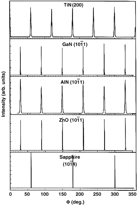
Figure 9.7 X-ray w scans of nitride compounds grown on sapphire substrate (0001). Reprinted
from R.D. Vispute, et al., Advances in pulsed laser deposition of nitrides and their integration
with oxides, Appl. Surface Sci. 127–129, 431. Copyright (1998) with permission from Elsevier
Structural Analysis 233
on ZnO. Ueda et al.
[12]
observed that the RHEED showed a ring pattern indicating that a
polycrystalline film had formed by a reaction between ammonia and the single crystal ZnO.
The (0002) reflection was predominant when the GaN films were grown with ZnO buffer
layer. An additional (112
1) reflection was observed along with (0002). In this sample sharp,
rock-like three-dimensional structures were observed.
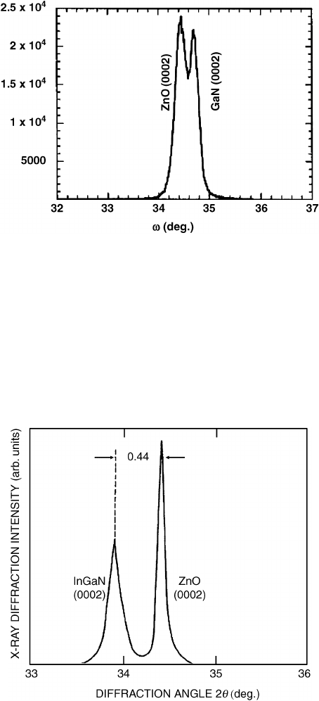
Figure 9.8 X-ray rocking curve of GaN on sapphire with ZnO buffer layer. Reprinted from R.D.
Vispute, et al., Advances in pulsed laser deposition of nitrides and their integration with oxides,
Appl. Surface Sci. 127–129, 431. Copyright (1998) with permission from Elsevier
Figure 9.9 X-ray rocking curve of InGaN/ZnO on sapphire substrate. Reprinted from
T. Matsuoka, N. Yoshimoto, T. Sasaki and A. Katsui, Wide-gap semiconductor indium gallium
nitride and indium gallium aluminum nitride grown by MOVPE, J. of Electro. Mater. 21, 157
(1992). Copyright (1992) with permission from Springer
234 Growth and Characterization
9.5 Surface Studies
For a comprehensive analysis of the properties of GaN films grown on ZnO subst rates,
a whole slew of surface sensitive techniques can be applied. For example, scanning
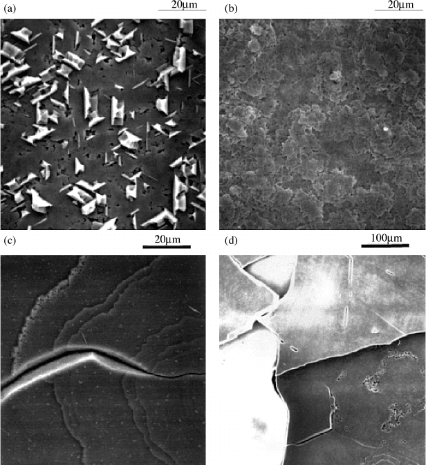
electron microscopy (SEM) analysis (Figure 9.13) showed that the GaN surface has large
grain sizes, but is smooth within the grains when the GaN is deposited with ZnO buffer on
sapphire substrates. Without ZnO buffer, however, the surface was found to be rough with
many small domains.
[12]
In this study, the surface of the Zn-face of ZnO was noted to be
smoother than that of the O-face. The rms roughness of the O-face surface is an order of
magnitude higher than that of the Zn-face. Surprisingly, the GaN layers g rown on the Zn-
face of ZnO are rough compared with those grown on O-face ZnO substrates.
[16]
The GaN
layers grown on ZnO substrates without any buffer layer at a substrate temperature above
760
C easily peeled off.
[16]
Therefore, the low temperature buffer layer was added to
prevent reaction between NH
3
and ZnO substrates. AFM images (Figure 9.1 4) show that
the surface of the GaN layers is smooth for when the GaN buffer was used whereas it is
rough for the AlN buffer case in part perhaps due to the higher lattice mismatch between
AlN and ZnO com pared with that of GaN and ZnO, but most likely due to the relatively
low surface mobility of Al as compared with Ga. Yun et al.
[37]
studied the growth of GaN
on different substrates without using GaN buffer layers. The GaN grown on the air
annealed O-face ZnO substrates showed uniform and densely populated flower-like
patterned surfaces with an rms value of 1.98 nm. The ZnO surface was also scanned by
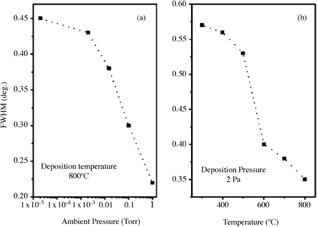
Figure 9.10 Variation of FWHM of XRD rocking curve for GaN/ZnO grown on sapphire vs (a)
ambient pressure and (b) deposition temperature. Reprinted from R. P. Wang, H. Muto, Y.
Yamada, and T. Kusumori, Effect of ZnO buffer layer on the quality of GaN films deposited by
pulsed laser ablation, Thin Solid Films, 411, 69. Copyright (2002) with permission from Elsevier
Surface Studies 235
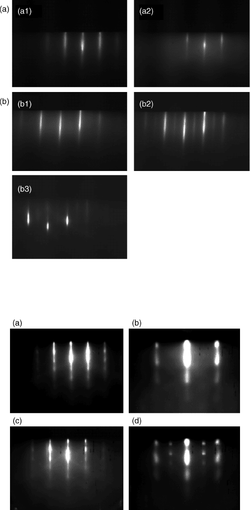
Figure 9.11 (a) RHEED patterns of O-face ZnO and GaN/ZnO: (a1) ZnO along
[11
02];
and
(a2) GaN along [
11
02
]. (b) RHEED pattern of GaN/ZnO: (b1) during growth (on Zn-face
ZnO); (b2) cooling down to 350
C (on Zn-face ZnO); and (b3) cooling down to 350
C (on
O-face ZnO)
Figure 9.12 RHEED patterns of ZnO and GaN/ZnO: (a) ZnO along [
2
110
]; (b) ZnO along
[
11
00
]; (c) GaN along [
2
110
]; and (d) GaN along [
11
00
]. Reprinted from R. P. Wang, H. Muto, Y.
Yamada, and T. Kusumori, Effect of ZnO buffer layer on the quality of GaN films deposited by
pulsed laser ablation, Thin Solid Films, 411, 69. Copyright (2002) with permission from Elsevier
236 Growth and Characterization
AFM, prior to the deposition of GaN, which showed smooth and sparsely scattered small size
granules with an rms value of 0.658 nm, as shown in Figure 9.15. TEM analysis showed that
the density of extended defects is in the order of 10
8
cm
2
on the surface of GaN, which is
about three orders of magnitude lower than that in the buffer layer region.
[16]
9.6 Optical Properties
9.6.1 Transmission Analysis
Optical measurements in general and transmission measurements in particular can be used
to discern various transitions taking place in films. In the case of GaN on ZnO, the direct
Figure 9.13 SEM images of (a) GaN/sapphire, (b) GaN/ZnO(25 nm)/sapphire, (c) GaN/ZnO
(200 nm)/sapphire and (d) the same as (c) but at different location. Reprinted from T. Ueda,
et al., Vapor phase epitaxy growth of GaN on pulsed laser deposited ZnO buffer layer , J. Cryst.
Growth, 187, 340. Copyright (1998) with permission from Elsevier
Optical Properties 237
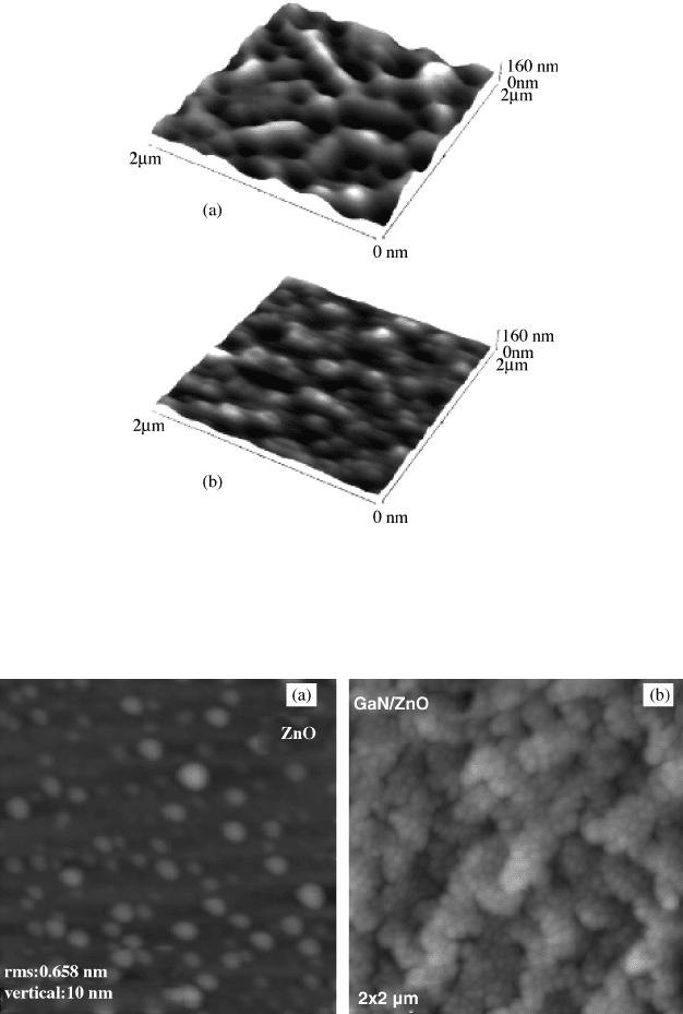
Figure 9.14 AFM images of (a) GaN grown on O-face ZnO, with AlN buffer and (b) GaN
buffer. Reprinted from F. Hamdani, et al., Microstructure and optical properties of epitaxial
GaN on ZnO (0001) grown by reactive molecular beam epitaxy, J. Appl. Phys., 83, 983.
Copyright (1998) with permission from American Institute of Physics
Figure 9.15 AFM images of (a) O-face ZnO and (b) GaN grown on O-face ZnO, without
buffer layer. Reprinted from F. Yun, M. A. Reshchikov, L. He, T. King, D. Huang, H. Morkoc¸, J.
Nause, G. Cantwell, H. P. Maruska, and C.W. Litton, Comparative analysis of MBE-grown GaN
films on SiC, ZnO and LiGaO
2
substrates, in Defect and Impurity Engineered Semiconductors
and Devices III, edited by S. Ashok, J. Chevallier, N.M. Johnson, B.L. Sopori and H. Okushi
(Mater. Res. Soc. Symp. Proc. Volume 719, Warrendale, PA, 2002) F8.21. Copyright (2002)
with permission from MRS
238 Growth and Characterization
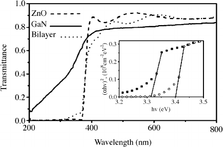
optical band gaps of 3.3 and 3.4 eV for ZnO and GaN, respectively, were observed by
optical transmission spectra.
[7]
A similar band gap value (3.45 eV) is reported for GaN
grown on ZnO/fused silica substrates by PLD.
[36]
Figure 9.16 shows sharp absorption edges for ZnO and GaN/ZnO except for GaN on
sapphire, indicating the high quality of the layers.
[10]
9.6.2 Cathodoluminescence Analysis
An electron beam can be used to create electron–hole pairs followed by observation of the
recombination processes in semiconductors such as GaN and ZnO. Because very high
excitation intensities can be obtained and the depth of the electron beam can be varied, this
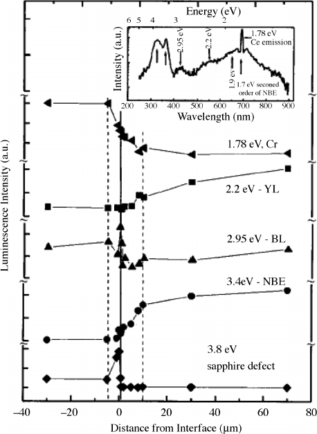
technique has been popular for analyzing GaN and ZnO. Sun et al.
[38]
studied defect levels
in the energy gap, emission positions and their intensities as a function of distance from
the GaN/ZnO interface in the samples, with different sheet densities (in the range of
6. 16.98.50810
14
cm
(2)
), grown by HVPE on ZnO buffered sapphire substrates by using
cathodoluminescence (CL) spectroscopy. The near band edge, blue emission, and yellow
luminescence peaks were observed at 3.4, 2.95 and 2.2 eV, respectiv ely, in the CL spectra at
room temperature (Figure 9.17). The intensities of the near-band-edge emission and yellow
emission increased as the raster center was moved from the interface towards the surface of the
GaN layer. Eventually, the dislocation density decreased with increasing distance from the
GaN/sapphire interface (d
int
) H 10 mm in sample 1 having a sheet interface concentration (n
s
)
of 6 10
14
cm
2
. Therefore, it can be asserted that the dislocations are not the sources for
yellow luminescence. Howe v er, they may decorate the complexes formed by Ga vacancies,
which are believed to be the source of this luminescence.
[39]
The broad blue luminescence(BL)
band pronounced at 2.9 eV for d
int
H 0.2 mm might be due to Zn participation because the
epitaxial layer was treated by ZnO buffer. The PL signature in GaN doped with Zn or
contaminated by Zn from prior uses of Zn was studied by Reshchikov et al.
[40]
The assessment
agrees well with the aforementioned BL emission in GaN grown on ZnO buffer layers or
Figure 9.16 Transmission spectra of ZnO, GaN and GaN/ZnO. The inset shows the band gaps of
3.3 and 3.4 eV related to ZnO and GaN, respectively. Reprinted from R. P. Wang, H. Muto, Y.
Yamada, and T. Kusumori, Effect of ZnO buffer layer on the quality of GaN films deposited by
pulsed laser ablation, Thin Solid Films, 411, 69. Copyright (2002) with permission from Elsevier
Optical Properties 239
substrates. Note that a similar in shape and position BL band is usually observed in GaN
heavily doped with Mg. However, it has a differen t origin and is att ributed to transitions
from a deep donor to a shallow Mg acceptor.
[41]
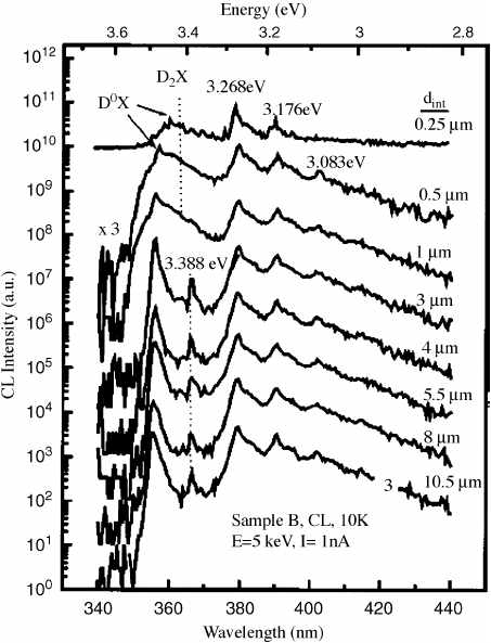
For sample 2, n
s
¼1.6 10
15
cm
2
,three
spectra are noted at different distances from the GaN/sapphire interface (d
int
¼0.3, 1 and
4 mm) at low tempera tures, as shown in Figure 9.18. The peak at 3.517 eV a bove the band
edge w as attributed to the free electron concentration at the degenerate interfacial layer.
[38]
The intensity of the peak decreased for d
int
¼1 mm and finally d isappeared for d
int
¼4 mm,
i.e. as the depth increased, the strong neutral donor bound exciton (D
0
X) emission
segregated at 3.483 eV. A shoulder on the D
0
X line at about 3.503 eV was assigned to
the excited state of th e free exciton.
[38]
The delineation of additional peaks, i.e. 3.41, 3.30,
3.28 and 3.19 e V, was o bserved as d
int
increased. The peak at 3.28 eV was related to the
donor–acceptor pair (DAP) recombination and its phonon replica is at 3.19 eV. The peak at
Figure 9.17 Cathodoluminescence intensity vs distance from the interface for different peaks;
sapphire defect, near-band-edge emission (NBE), blue emission (BL), yellow luminescence
(YL), chromium (Cr) from sapphire (sample 1, n
s
¼6 10
14
cm
2
). Note that the scans are nor
normalized to a constant value and the GaN/sapphire interface is referenced as d
int
¼0.
Reprinted from X. L. Sun, et al., Depth-dependent investigation of defects and impurity doping
in GaN/sapphire using scanning electron microscopy and cathodoluminescence spectroscopy.
J. Appl. Phys., 91, 6729. Copyright (2002) with permission from American Institute of Physics
240 Growth and Characterization

3.41 eV freque ntly appears in GaN and is attribute d by Xia et al.
[36]
to excitons bound
to stacking faults. The peak at 3.30 eV could be due to either ZnO or GaN cubic phase
mixed wit h th e hexagonal phase.
[38]
Figure 9.19 shows the CL s pectra of samp le 3,
n
s
¼9.8 10
15
cm
2
.
In the case of sample 4, n
s
¼5 10
16
cm
2
and 17 mm thickness, the sapphire substrate
was nitridated prior to GaN growth. In the low temperature CL spectra, D
0
X at 3.483 eV
was predominant as the depth increased from the interface and the other two known peaks
at 3.4 and 3.3 eV are ascribed to excitons bound to stacking faults and or a cubic GaN
domain. At the interface (d
int
5 mm), the 3.563 eV peak is due to band filling at the
degenerate doping levels and the free-electron recombination.
[38]
The same feature has
been observed in heavily doped (10
19
cm
2
) samples.
[42]
The D
0
X emission intensi ty
decreased when CL spectra were recorded for columns or columnar regions, which might
be due to grain boundaries, or high defect levels which can act as efficient nonradiative
recombination centers.
Both samples 2 (1.6 10
15
cm
2
) and 3 (9.8 10
15
cm
2
) showed free excitons in the
CL spectra which have been attributed to the quality of the samples. A weak residua l
acceptor level peak is seen in the luminescence spectra of these samples. This could be due
to either Ga vacancy or C.
[38]
In sample 4, the near-band-edge emission quenches near the
interface and grain boundaries where very high defect densities appear. A broad emission
band at 3.56 eV is likely due to free electron recombination band showing high degenerate
doping near the interface and grain boundaries (Figure 9.20).
Figure 9.18 CL spectra of sample 2 (n
s
¼1.6 10
15
cm
2
) at different interface distances.
Reprinted from X. L. Sun, et al., Depth-dependent investigation of defects and impurity doping
in GaN/sapphire using scanning electron microscopy and cathodoluminescence spectroscopy.
J. Appl. Phys., 91, 6729. Copyright (2002) with permission from American Institute of Physics
Optical Properties 241
9.6.3 Photoluminescence Analysis
Similar to the case of high energy electron induced electron–hole pair generation, above
gap photon excitation can also be used to follow carrier recombination in an effort to
determine the quality and optical processes taking place in the layers. Photoluminescence
(PL) of three sets of bulk ZnO samples grown by Air Force Laboratories (Hanscom),
Cermet, Inc., and what was then the Eagle Picher Company to use as substrates for GaN
growth have been studied. All samples demonstrated good optical quality with very high
quantum efficiency. Therefore, the quantum efficiency of the Cermet sample in the near-
band-edge region exceeded 20%. The PL spectrum at 10 K of this sample is shown in
Figure 9.21. The crystal quality of the sample was confirmed to be good by PL spectra
showing low FWHM of 0.55 meV for the peak at 3.3597 eV. This peak is tentatively
attributed to the exciton bound to neutral donor. Identification of the exciton structure of
ZnO is quite controversial in the literature, so further studies are required. The main peak
at 3.36 eV was repeated three times on the low-energy tail of the exciton emission at
energies which are multiples of the LO phonon energy (about 71 meV). Another sharp
Figure 9.19 CL spectra of sample 3 (n
s
¼9.8 10
15
cm
2
) at different interface distances.
Reprinted from X. L. Sun, et al., Depth-dependent investigation of defects and impurity doping
in GaN/sapphire using scanning electron microscopy and cathodoluminescence spectroscopy.
J. Appl. Phys., 91, 6729. Copyright (2002) with permission from American Institute of Physics
242 Growth and Characterization