Lima J.J.Pedroso, de (ed.). Nuclear Medicine Physics
Подождите немного. Документ загружается.

138 Nuclear Medicine Physics
SPECT PET
Tomographic images
Multiple
images
Image
reconstruction
Multiple
images
Camera
rotation
Planar images
Yes
No
(electronic
collimation)
Two 511 keV
photons
emitted
simultaneously
in opoosite
collections
1 γ photon
99m
Tc: 140 keV
other energies
depending on
radioisotope
1 γ photon
1 position
γ emitter
β
+
emitter
Scintigraphy
Colimator
γ
γ
γ
Detection
Labelling
Decay
Image
reconstruction
Tomographic images
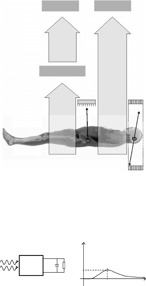
FIGURE 5.1
Comparison between in vivo imaging methods in nuclear medicine, with regard to the detection
and production of images. The presence of the collimator for planar scintigraphy and SPECT
imaging, which is required in order to locate the radioactive source in relation to the detec-
tor, causes a very significant loss of sensitivity in comparison with PET and degrades spatial
resolution, which deteriorates in proportion to the distance from the radioactive source to the
detector.
V
R
C
t
Detector
Q/C
FIGURE 5.2
Diagram of the equivalent circuitry connected to the detector and the typical voltage (V) response
of the circuitry.

Radiation Detectors and Image Formation 139
load circuit. The amplitude of the signal is proportional to the deposit charge
in the detector (V
max
= Q/C). For each efficient interaction taking place in the
detector, there is a corresponding electrical pulse in the measuring circuit and
the pulse rate is, therefore, equivalent to the interaction rate in the detector.
Efficiency, energy resolution, and dead time are important factors in radi-
ation detectors. The efficiency of a detector links the number of photons
entering the active volume with the number of electrical impulses gener-
ated. For convenience, efficiency is studied in two separate ways: as absolute
efficiency and as intrinsic efficiency. Absolute efficiency is defined as the ratio
between the number of pulses and the measured number of photons emitted
by the source [4]:
ε
abs
=
number of measured pulses
number of emitted photons
. (5.1)
Conversely, intrinsic efficiency is defined by taking into account only the
characteristics of the detector and, hence, is independent of the geometri-
cal characteristics of the measuring arrangement. Thus, intrinsic efficiency is
defined by
ε
int
=
number of measured pulses
number of incident photons in detector
. (5.2)
Considering a point source emitting isotropically, the relationship between
the two efficiencies is based only on geometrical arguments and is given by
ε
int
=
4π
Ω
ε
abs
, (5.3)
where Ω is the solid angle of the detector seen from the position of the point
source. Intrinsic efficiency depends on the material of the detector, the thick-
ness (measured in terms of the direction of the incident radiation), and the
energy of the incident radiation.
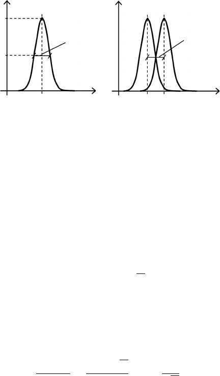
The energy resolution of a detector is defined as the ability to discriminate
between two close radiation energies. The response of a detector to a real
monoenergetic source is not a narrow peak (mathematically, a delta function)
but a Gaussian distribution whose amplitude corresponds to the radiation
energy.
Formally, the energy resolution is given by the ratio between the full width
at half maximum (FWHM = ΔE) of the energy response of the detector to
monoenergetic radiation and the peak energy (E
p
) [4]. Two monoenergetic
sourcesare distinguished by a detector if the differencebetween their energies
is greater than the FWHM of the response curve (Figure 5.3).
Several factors contribute toward the deterioration of energy resolution in
a detector, such as statistical noise due to the discrete nature of the signal,
the noise caused by the detector and by the measuring circuit, and any devi-
140 Nuclear Medicine Physics
FWHM
H/2
(a) (b)
H
dN/dE
FWHM
E
EE
p
FIGURE 5.3
(a) Response curve for a source point obtained by a real radiation detector. The xx axis represents
the energy of the signal, whereas the yy axis is the number of counts per interval of energy. (b)
Diagram of the minimum difference in energy that must exist in order to discriminate between
two monoenergetic sources.
ations from operating conditions during measurement. Although the latter
two sources of error are likely to be minimized by optimizing the detector, the
primary cause of noise is always present regardless of the detector. Statistical
noise is related to the fact that the charge deposited in the detector is discrete,
as it depends on the number of charge carriers. The number of charge carriers
is random and follows a certain distribution of probabilities. Assuming that
the process follows a Poisson distribution, for a given number N, of created
charges, the expected standard deviation is
√
N. Assuming further that the
response of the detector is linear to the number of charges generated, the
expected deposited energy (E
0
) should be equal to KN, where K is a constant
of proportionality. For a high number N of charges, the response of the detec-
tor follows a Gaussian distribution. For this distribution, the FWHM is equal
to 2.35σ, hence;
R =
FWHM
E
0
=
2.35K
√
N
KN
= 2.35
1
√
N
. (5.4)
This relationship implies that statistical noise limits the energy resolution,
which can be improved if the number of charges per event increases.
The dead time of a detector is usually defined as the time that should exist
between two separate events so that they can be measured as two different
electrical signals. Depending on the type of detector, the limiting factor is
either the detection process or the associated electronic circuit.
5.1.1.1 Interaction of Radiation with Matter
When gamma (or x) rays focus directly on an object and cross it, some photons
interact with the particles of the object and their energy can be absorbed or
Radiation Detectors and Image Formation 141
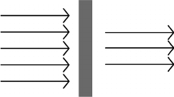
scattered. The process of absorption and dispersion of radiation is generally
known as attenuation (Figure 5.4).
The intensity (energy per unit areaand per unit time) of the radiation emerg-
ing from the object is less than the incident intensity, and the fraction of
transmission depends on the density, atomic number, and thickness of the
material and the radiation energy.
The attenuation resulting from the interaction of gamma radiation with the
particles of the medium is not a unique process—a single interaction rarely
results in the incident photon changing to another form of energy. Usually,
several interactions are needed until all the photon energy is transformed.
Therefore, attenuation results from all processes involved, that is, the pho-
toelectric effect, the Compton effect, the Rayleigh–Thomson effect and, for
energies above 1.022 MeV, the production of pairs.
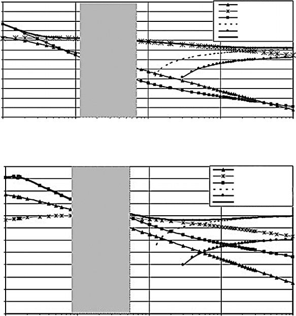
Figure 5.5 shows the total attenuation coefficient for water and for lead
in terms of incident gamma radiation energy. The usual range of energies
for gamma radiation in NM is 80–511 keV, corresponding approximately to
the shaded area in the chart. For water (the main constituent of biological
tissues), the predominant effect in the energy range in question is the Comp-
ton effect, and the occurrence of the photoelectric effect is much smaller. On
the other hand, for lead the photoelectric effect is predominant in the same
energy range. The total attenuation of water is low, which is fundamental to
the success of PET and SPECT imaging, whereas the attenuation character-
istics of lead are essential for collimators and the shielding devices used in
radioprotection.
The photoelectric effect occurs when the incident photon transfers its total
energy to an electron of an atom, which is ejected with a kinetic energy equal
to the difference between the energy of the incident photon and the binding
energy (E
c
= hν −E
). The ejection of the electron causes the atom to become
an ion for a short period of time. This excited state remains until a more
energetic electron occupies the hole created, emitting a photon with energy
that is equal to the difference between the energies of the initial and final
I = I
0
e
–μ x
I
0
I
FIGURE 5.4
Illustration of how the attenuation experienced by a monoenergetic beam when crossed by an
object of thickness x. I
0
is the intensity of the incident radiation beam, reduced to I after crossing
the object. The reduction fraction is given by e
−μx
, where μ is the linear attenuation coefficient
of the medium crossed by the radiation.
142 Nuclear Medicine Physics
1.0E+03
μ (cm
3
/g)
μ (cm
3
/g)
Lead attenuation coefficient for different energies
Water attenuation coefficient for different energies
Rayleigh effect
Compton effect
Photoelectric effect
Pairs production (nuclear)
Pairs production (atomic)
Total attenuation
Rayleigh effect
Compton effect
Photoelectric effect
Pairs production (nuclear)
Pairs production (atomic)
Total attenuation
1.0E+02
1.0E+01
1.0E+00
1.0E–01
1.0E–02
1.0E–03
1.0E–04
1.0E–05
1.0E–06
1.0E–07
1.0E–08
1.0E–09
1.0E+03
(a)
(b)
1.0E+02
1.0E+01
1.0E+00
1.0E–01
1.0E–02
1.0E–03
1.0E–04
1.0E–05
1.0E–06
1.0E–07
1.0E–08
1.0E–09
1.0E–02 1.0E–01 1.0E+00
Energy (MeV)
1.0E+01 1.0E+02
1.0E–02 1.0E–01 1.0E+00
Energy (MeV)
1.0E+01 1.0E+02
FIGURE 5.5
(a) Variation of the water attenuation coefficient with energy. The total attenuation is the com-
bined effect of the four mechanisms. (Data from: http://physics.nist.gov/PhysRefData/Xcom/
html/xcom1.html.) (b) Variation of the lead attenuation coefficient with energy. The total atten-
uation is the combined effect of the four mechanisms. (Data from: http://physics.nist.gov/
PhysRefData/Xcom/html/xcom1.html.)
states of the electron. The radiation emitted, which is generally termed char-
acteristic x-ray, is usually absorbed later by the detector. The probability of
the occurrence of the photoelectric effect depends on the fourth power of the
atomic number (Z), which is easily observable in Figure 5.5.
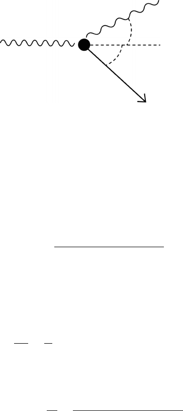
The Compton effect or Compton scattering, occurs when a photon interacts
with an electron, causing deflection of the photon, which sends part of the
energy to the electron that recoils (Figure 5.6).
The relationship between the energy of the photon, E
0
, before interacting
with the electron and the energy of the deflected photon, E
, for a given angle
Radiation Detectors and Image Formation 143
Recoil electron
Incident photon
Scattered photon
E′ = hv ′
E
0
= hv
φ
θ
FIGURE 5.6
Diagram showing the Compton effect—the interaction of a photon with an electron results in
the deflection of the photon, which transfers energy to the electron. This interaction results in
a scattered photon with lower energy (longer wavelength) and the recoil of the electron. (Data
from http://physics.nist.gov/PhysRefData/Xcom/html/xcom1.html.)
θ can be obtained from the law of conservation of linear momentum and the
law of conservation of energy. The application of these laws results in the
expression:
E
=
E
0
1 +(E
0
/m
e
c
2
)(1 −cos θ)
, (5.5)
where m
e
c
2
is the energy of the electron at rest.
Compton scattering is anisotropic, that is, the probability of a photon being
deflective is not equal in all directions. The Klein–Nishina formula describes
scatter probability in terms of direction:
dσ
dΩ
=
r
2
e
2
P
E
0
,θ
−P
2
E
0
,θ
sen(θ) +P
3
E
γ
,θ
, (5.6)
where r
e
is the classical electron radius and P
E
0
,θ
is the ratio of the energies
before and after Compton deflection:
P
E
0
,θ
=
E
E
0
=
1
1 +(E
0
/m
e
c
2
)(1 −cos θ)
. (5.7)
The value dσ/dΩ is usually known as the differential cross section and
represents the probability of a photon being scattered in the solid angle dΩ.
Rayleigh–Thomson scattering is also known as elastic scattering, as the
kinetic energy is conserved. The probability of this effect occurring is greater
for low-energy photons (<10 keV) that are deflected with no loss of energy
when interacting with an atom.
Since pair production is an interaction mechanism that occurs when the
energy is greater than 1.022 MeV, it is therefore, not observed in the energy
144 Nuclear Medicine Physics
ranges associated with NM. The pair production mechanism can be sum-
marized as the interaction of a high-energy photon with the nucleus field
or the electron field in which the photon is annihilated, producing an
electron–positron pair.
Photoabsorption is a mechanism that occurs only with high-energy pho-
tons, in which a photon is captured by the nucleus, which then de-excites
emitting one or more particles.
5.1.2 Gamma Radiation Detectors
The success of detection depends on the efficacy of the radiation interaction
with the detector, because what is actually measured are the products of inter-
action. Measurement is mainly based on the fast electrons that result from the
interaction of radiation with matter.The maximum energyof these electrons is
equal to the energy of the incident photon; the electrons gradually lose their
energy through interaction with the atoms of the medium that are ionized
or excited. The charge produced is collected either directly via proportional
counters or semiconductor detectors or indirectly via crystal scintillators.
5.1.2.1 Gas-Filled Detectors
Gas-filled detectors are composed of two electrodes separated by a gaseous
atmosphere. Generally, the container that encloses the gas is one of the elec-
trodes (cathode), and the other electrode (anode) is a thin wire running
through the center of the system [4] (Figure 5.7).
Gamma radiation interacts with the gas contained in the detector causing,
in certain circumstances, ionization and the consequent ejection of electrons.
These are accelerated toward the anode and, if fully collected by the anode,
produce a measurable electric current. Hence, the detector operates as an
ionization chamber.
When the external voltage transfers enough kinetic energy to electrons,they
produce new ionized atoms emitting more electrons—the avalanche effect.
The negative charge created during this process is then collected by the anode,
causing an electrical impulse which is the signal that is actually measured
(see Section 5.1.1). For a certain range of the electric field, the signal obtained
is proportional to the number of electron–ion pairs generated by incident
radiation. In this case, the detector is designated as a proportional counter
and operates in the proportionality region, which represents the conventional
mode of operation for these detectors.
In sufficiently high electric fields, the avalanche effect extends to the entire
anode, which leads to a loss of proportionality in the relationship between
the charge produced and the energy released by the incident radiation. The
signal from the detector always has the same amplitude, therefore meaning
that the detector operates in the Geiger–Müller region.
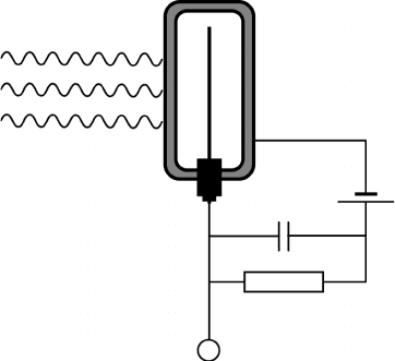
Radiation Detectors and Image Formation 145
Signal
R
C
V
FIGURE 5.7
Equivalent circuit diagram of a gas detector. The electric field created within the detector acceler-
ates the electrons produced by the interaction of radiation with the gas, which are then collected
at the anode (internal wire).
5.1.2.2 Semiconductor Detectors
The semiconductor detector most commonly used in the detection of gamma
radiation is the germanium–lithium detector. This type of detector has been
used in gamma radiation spectroscopy since the 1960s. In comparison with
gas detectors, these detectors offer the advantage of a smaller size and larger
density. An additional interesting feature is the excellent energy resolution.
However, until recently, these detectors required a cooling device in order
to operate efficiently, which limited their use in medical imaging. With the
emergence of detectors such as the CdZnTe (CZT), which can operate at room
temperature, this limitation has disappeared and gamma cameras using these
semiconductor detectors are now available. Nevertheless, the energy resolu-
tion of CZT detectors is lower than that of germanium detectors, although
still higher than scintillator detectors. There are also solid-state detectors (sil-
icon) that require no cooling devices but can only be used with low-energy
radiation (tens of keV).
The working principle of semiconductor detectors is based on the formation
of electron–hole pairs whose displacement leads to a measurable electrical
signal.
A semiconductor can be defined as a solid whose valence band is complete
whenT = 0 K but whose forbidden band isso small (few eV) that electronscan
be easily thermally excited (at room temperature) and pass to the conduction
band [5]. If the forbidden band is larger, the number of electrons capable
of moving to the conduction band is much smaller and the material is then
classified as an insulator.
146 Nuclear Medicine Physics
For each electron excited to the conduction band in a semiconductor, a hole
is created in the valence band whose mobility is only a fraction of the mobility
of the electrons. In this situation, conduction of an electric current may exist
if an electric field is applied. However, the electric conductivity is lower than
that of metal materials and depends on temperature.
A semiconductor that is free of impurities has an equal number of electrons
in the conduction band and holes in the valence band, as the electrons are
thermically excited; and there is a one-to-one relationship between electrons
and holes. A semiconductor with these characteristics is known as intrinsic
or undoped. Considering the concentration of electrons (n) in the conduction
band and the concentration of holes (p) in the valence band, it can be easily
inferred that, for an intrinsic semiconductor:
n = p. (5.8)
The doping of pure semiconductors with appropriate impurities leads to
situations in which the previous relationship is not maintained and, con-
sequently, there may be an excess of electrons or an excess of holes. The
materials obtained by this process are known as n-type semiconductors or
p-type semiconductors, respectively.
A semiconductor with two adjacent regions, a p-region and a n-region,
demonstrates properties suitable for use as radiation detector. In the pn junc-
tion, there is diffusion of electrons from the n to the p region and a diffusion of
holes in the opposite direction. This process creates a voltage difference in the
pn junction. Near the pn junction, a region is created—the depletion region—
in which thereis balance of chargecarriers. The depletion region has favorable
features as a means of detecting radiation, as any electron that is created in
this region is accelerated into the n side and any created hole is accelerated
into the p side. However, in a nonpolarized pn junction, the depletion region
is small and the junction capacitance is high; hence, the spontaneous electric
field generated is of low intensity and does not allow the charge carriers to
move quickly. For these reasons, the pn junction is generally polarized when
used as a radiation detector in real applications.
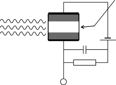
Figure 5.8 shows a diagram of a typical semiconductor detector. The radia-
tion interacts with the detector, perhapscausing ionization and, therefore, free
charges, which are accelerated by the imposed electric field. The charge cre-
ated is then collected by the polarization electrodes, generating an electrical
signal.
The incident photons are absorbed at the pn junction of the semiconductor
crystal, which is affected by a high-voltage difference, creating a large number
of electron–hole pairs. For each electron–hole pair produced, approximately
3–5 eV are expended on average, and the total number of pairs is proportional
to the gamma photon energy. With NaI (Tl) crystal, about 30 eV are needed to
create one ionization and to produce one scintillation within the crystal. The
number of electron–hole pairs produced is about 6–10 times greater than the
amount of scintillation.
Radiation Detectors and Image Formation 147
Signal
Depletion region
R
C
V
n
p
FIGURE 5.8
Equivalent circuit diagram of a semiconductor detector. The detector is an inversely polarized pn
junction. When the gamma radiation produces an electron–hole, the charge is conducted through
the sensitive region (depletion region) generating a measurable signal.
The energy resolution of the CZT gamma camera is approximately 5%,
compared with about 14% for the NaI (Tl) gamma camera. The fact that the
CZT gamma camera does not use photomultiplier tubes (PMT) is also an
advantage.
The most recent CZT crystals are slightly more efficient than NaI (Tl). The
intrinsic spatial resolution of CZT gamma cameras is also greater, being
approximately 2–3 mm compared with 3–4 mm for the NaI (Tl) gamma
cameras, at 140 keV.
In addition, the collection time for the electron–hole pairs is at least 100
times shorter than the decay time of the scintillation crystal NaI (Tl), which
allows for an increase in the counting speed (250,000 count/s).
The CZT camera weighs about 100 times less, is considerably smaller than
the scintillation camera, and can, therefore, be easily moved between different
hospital departments.
These differences result in several advantages for image quality, such
as improved contrast due to greater efficiency, higher energy resolution,
and accuracy of position determination (intrinsic resolution), which is also
enhanced as an effect of the modular structure [6].
5.1.2.3 Scintillation Detectors
Scintillators convert high-energy gamma photons into photons with wave-
length in the visible range, which, in turn, are detected using PMT. The PMT
collect the light created in the crystal by the γ rays, generating electrical sig-
nals that contain information about the energy of the interactions taking place
in the crystal.