Kounadis A.N., Gdoutos E.E. (Eds.) Recent Advances in Mechanics
Подождите немного. Документ загружается.


Recent Advances in Microelectromechanical Systems and Their Applications 259
such, is critical to implementation of this methodology for development of MEMS
as discussed herein.
Therefore, to minimize this influence, a number of algorithms for determination
of Ω were developed. Some of these algorithms require multiple recordings of
each of the two states, in the case of double-exposure method, of the object being
investigated with introduction of a discrete phase step between the recordings
[3,33]. For example, the intensity patterns of the first and the second exposures,
I
n
(x,y) and I’
n
(x,y), respectively, in the double-exposure sequence, can be
represented by the following equations [7]:
() ()()
()
[]
()
[]
{}()
[]
{}
nro
ron
yxyxIyxI
yxIyxIyxI
θϕ
+Δ+
++=
,cos,,2
,,,
2/1
(6)
and
() ()() ()
[]
()
[]
{}
()
[]
(){}
,,,cos
,,2,,,
2/1
'
yxyx
yxIyxIyxIyxIyxI
n
roron
Ω++Δ×
×++=
θϕ
(7)
where I
o
(x,y) and I
r
(x,y) denote the object and the reference beam intensities,
respectively, with (x,y) representing spatial coordinates, Δφ(x,y) = φ
o
(x,y)- φ
r
(x,y)
is the optical phase difference based on φ
o
(x,y), denoting random phase of the light
reflected from an object, and φ
r
(x,y), denoting the phase of the reference beam, θ
n
represents the discrete applied n
th
phase step, and Ω(x,y) is the fringe-locus
function relating to the displacements/deformations that an object incurred
between the first and the second exposures; Ω is what we need to determine.
When Ω is known, it is used in Eq. 2 to find L.
In the case of the 5-phase-steps algorithm with θ
n
=0, π/2, π, 3π/2, and 2π, the
distribution of the values of Ω(x,y) can be determined using [7]
()
() ()
[]
()()()
.
,,,2
,,2
tan,
513
42
1
⎭
⎬
⎫
⎩
⎨
⎧
−−
−
=Ω
−
yxIyxIyxI
yxIyxI
yx
(8)
Results produced by Eq. 8 depend on capabilities of the illuminating, the
imaging, and the processing subsystems of the OEH system used in a specific
application. Developments in laser, fiber optic, CCD camera, and computer
technologies have led to advances in the OEH methodology; in the past, these
advances have almost paralleled the advances in the image recording media [34].
These developments resulted in educational procedures [2] and led to MEMS
education alliance [35].
In response to the needs of the emerging MEMS technology, an optoelectronic
laser interferometric microscope (OELIM) system for studies of objects with
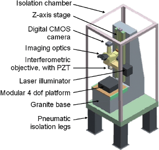
micron size features was developed [36,37], Fig. 12.
260 R.J. Pryputniewicz
Fig. 12. OELIM configuration used herein.
3.3.1 OELIM System
In the OELIM system, Fig. 12, light beam produced by a laser illuminator is
directed into a directional beam splitter cube, which produces an object beam that
is sent into an interferometric objective with PZT phase stepper controlled
microscope lens. The lens, in turn, illuminates MEMS being investigated. The
particular characteristic of the configuration shown is that its specially designed
interferometric objective has a long working distance providing ample space for
installation of an environmental chamber and/or other loading device(s), as
needed to characterize various MEMS.
It should be noted that in the implementation of the OELIM system used in this
study, the environmental chamber permitted simultaneous control of pressure/
vacuum, temperature (heating and cooling), as well as dynamic excitation (needed
for vibrations) of the test samples being characterized/developed.
In the configuration of Fig. 12 the object beam reflected by the MEMS passes
back through the objective to the beam splitter cube where it is combined with a
reference beam. The two beams, recombined at the beam splitter, are imaged onto
the sensing element of a CCD camera, which digitally records intensity
distributions of the resulting interference patterns. These patterns are transferred
to the system computer for subsequent quantitative processing to determine Ω(x,y)
according to Eq. 8, which is needed to determine L based on the use of Eq. 2.
Recent Advances in Microelectromechanical Systems and Their Applications 261
4 Representative Results
The optoelectronic methodology described in the preceding Section was used to
determine displacements and deformations of the MEMS samples described in the
Section 2. Results of these determinations are summarized in Sections 4.1 to 4.4,
respectively.
4.1 Motions of HRS Microengine
Using the analytical model [8,13,32], forces acting on the microengine during its
operation were calculated to be a nonlinear function of rpm indicating that the
force increases at an increasing rate as the rotational speed of a microengine
increases; for example this function indicates that at 6,000 rpm magnitude of the
force acting on a connecting pin is 4 nN while at 500,000 rpm it is 27 μN.
Forces generated during operation of a microengine, load the drive gear and make
it wobble as it rotates around its shaft. A unique capability to measure this wobble is
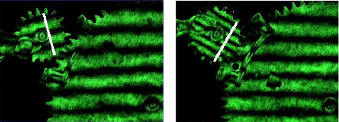
provided by the OELIM methodology. Typical results obtained for two different
positions in a rotation cycle of the drive gear are shown in Fig. 13, where fringe
patterns vividly display changes in magnitude and direction of the displacements of
the microgears. These displacements, based on the fringe patterns of Fig. 13 vary in
magnitude from 0.8 μm to 1.7 μm, respectively; it should be noted that, in
comparison with these displacements, thickness of gears is about 2 μm. These
variations in displacements are due to kinematics and kinetics caused by impulsive
loading forces generated by the input signals during rotational/operational cycle. In
addition, the experimental results show that the wobble depends on the angular
position in the rotation cycle, which can be related to the forces exerted on the drive
gear by the pin during a typical operational cycle.
Fig. 13. Representative OELIM fringe patterns recorded during the study of dynamic
characteristics of microengines, at two different positions in a rotation cycle. White lines
indicate locations (a) and (b) where measurements of displacements, quoted in the text,
were made.
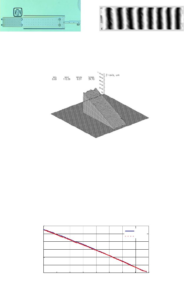
Operational functionality of a micromirror system depends also on the quality
of motions of section AB of the hinged micromirror, Fig. 14. OELIM was used to
measure these motions by recording fringe patterns, Fig. 15, which were, in turn,
interpreted to determine deformations/motions of the section AB of the
micromirror, Fig. 16.
(a) (b)
262 R.J. Pryputniewicz
AB
__
100 µm
Fig. 14. Measurements were made on the
AB section, 100 μm wide and about 400 μm
long, of a hinged micromirror.
Fig. 15. Representative OELIM fringe pattern
of the AB section of a hinged micromirror,
shown in Fig. 14.
Fig. 16. Wireframe representation of absolute shape and deformations/motions of the
section AB of a hinged micromirror, corresponding to the upright position displayed in Fig.
3. Measurements show that the micromirror displacements range from 0 μm at hinge B to
113 μm at hinge A at which there is also a tilt of 18 mrad, based on results of Fig. 17.
Using Fig. 16, detailed information about deformations/motions of a
micromirror can be obtained, Fig. 17. This figure displays traces that were made
parallel to the long edges of section AB of the micromirror. Noticeable
differences between the two traces were measured and led to estimate of a tilt of
18 mrad at the hinge A.
0
20
40
60
80
100
120
0 50 100 150 200 250 300 350 400
X- P O S I TIO N, µ m
Z-POSITION, µ
m
y=4 µm
y=95 µm
Fig. 17. Vertical displacements (Z-POSITION) of section AB as a function of position
along the length (X-POSITION) of a micromirror as determined from traces parallel to the
long edges of the wireframe display of Fig. 16, resulting tilt of 18 mrad was determined at
hinge A (on the left side) of section AB shown in Fig. 14.

Recent Advances in Microelectromechanical Systems and Their Applications 263
4.2 Deformations of a Microgyroscope
Deformations of proof masses/shuttles were measured during operation of a
microgyroscope. In this application, interferograms were recorded stroboscopically
while microgyros were driven at their operating frequencies. To facilitate these
recordings, the optoelectronic system was set up to be sensitive to the out-of-plane
motions. Representative interferograms, corresponding to deformations of the left
shuttle, while a microgyro was operating at 10.1 kHz are shown in Fig. 18.
Observation of the fringe patterns of this figure clearly indicates asymmetry in
deformations of the proof mass(es) of a microgyroscope. This can be related to
structural design and suspension of the shuttles as well as to the way that
electrostatic forces affect their motions and deformations. A representative
display of deformations of the left shuttle of a microgyro operating at 10.1 kHz,
during a specific instant in a vibration cycle, is given in Fig. 19, indicating
deformations ranging up to 212 nm, which ideally should not exist. However, the
deformations/motions were measured, in this case, to be orders of magnitude
greater than typical (magnitudes of) motions of the proof masses due to the
Coriolis forces.
Fig. 18. Representative OELIM fringe patterns of the
left shuttle, at different times in a vibration cycle,
while a microgyro is operating at 10.1 kHz.
Fig. 19. The out-of-plane 212 nm
deformation component of the left
shuttle, based on Fig. 18.
Accuracy and precision of a microgyro depends on the quality of its
suspension. This suspension is provided by folded springs attached, at one end, to
proof masse/shuttle and, at the other end, to a post forming a part of a substrate,
Fig. 20a. Any deformations of the springs that are not in response to functional
operation of a sensor will cause an incorrect (i.e., erroneous) output. For example,
thermomechanical distortions of a package affect shape of posts and these, in turn,
lead to undesired deformations of the springs and erroneous results produced by a
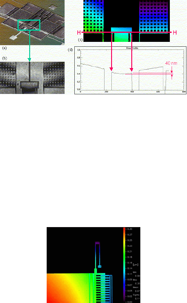
sensor supported by these springs [3]. Because of the nanoscale of these
deformations and microsize objects over which they take place, it was not until the
advancement of optoelectronic metrology that such deformations were quantified
in the FFV, Fig. 20. This figure shows that the thermomechanical deformations of
a post are on the order of 40 nm [37].
Functional operation of MEMS microgyros (usually) depends on motion of a
proof mass in response to an applied load. The proof masses of a microgyro are
(typically) suspended by folded springs: one spring in each corner of a proof
264 R.J. Pryputniewicz
Fig. 20. OELIM measurements of thermomechanical deformations of a post in a
microgyro: (a) dual shuttle configuration with the rectangle indicating one of the posts, (b)
interference fringe pattern over the post section selected in part (a), (c) contour
representation of deformations corresponding to the fringe pattern shown in part (b) -
horizontal line HH indicates the trace along which deformations of the post were
determined, (d) deformations determined along the line HH of part (c).
mass/shuttle, Fig. 5. Because of advances in design, suspension springs that have
several folds (or turns) were implemented. These multi-fold spring configurations
allow compact design of MEMS, which facilitates a fast response. Figure 21
displays representative deformations of the upper-right folded spring supporting
the left proof mass of a microgyro, as measured using the OELIM methodology
[38]. These deformations are about 300 nm, over the section of the microgyro
displayed in the figure. More specifically, the folded spring, shown in Fig. 21,
deforms approximately 126 nm between the point where it is attached to the post
and the point of its attachment to the proof mass. The proof mass itself has the
deformation of about 174 nm. To mitigate adverse effects of packaging, new
design/fabrication approaches are being developed [39].
Fig. 21. OELIM measured thermomechanical deformations of the upper-right section of the
left proof mass of a MEMS gyroscope, Fig. 5, maximum deformation is 300 nm: 2D
contour representation.
Recent Advances in Microelectromechanical Systems and Their Applications 265
4.3 Deformations of a Pressure Sensor
Using the specially designed test fixture, the MEMS PPSs were subjected to high
pressure side (HPS) and low pressure side (LPS) loads [17,40]. These loads
ranged from the rest (i.e., reference) pressure, set at atmospheric, up to 100 psig
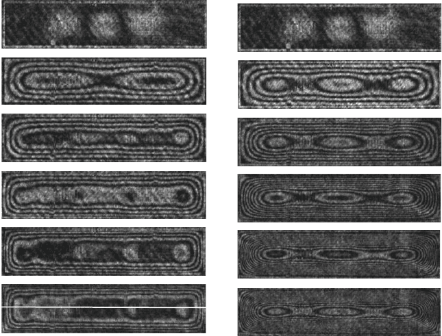
[41]. Representative OELIM fringe patterns, corresponding to deformations of the
diaphragms subjected to these loads, are shown in Figs 22 and 23.
It should be noted that the absolute shapes of the diaphragms at rest, Figs 22a
and 23a, influence their response to the applied pressures. That is, deformed
shapes of a specific diaphragm are different under HPS and LPS loads of the same
magnitude as, e.g., can be seen comparing Figs 22b and 23b. Both of these figures
show OELIM fringe patterns of the diaphragms subjected to the loads having the
magnitude of 10 psig. Based on previous studies [17], deformations of the
diaphragms due to HPS and LPS loads of this magnitude are unobstructed. Yet,
the fringe patterns vividly indicate different deformation patterns because of
influence that the initial shape, due to the residual stresses that developed while
fabricating these MEMS, has on their operational performance.
Clearly, as the load magnitudes increase so do the deformations of the diaphragms.
(a
)
(b
)
(c
)
(d
)
(e
)
(f
L
L
(a
)
(b
)
(c
)
(d
)
(e
)
(f
Fig. 22. Representative OELIM fringe patterns
corresponding to the HPS loadings of: (a) 0
psig (rest state), (b) 10 psig, (c) 20 psig, (d) 40
psig, (e) 80 psig, and (f) 100 psig.
Fig. 23. Representative OELIM fringe patterns
corresponding to the LPS loadings of: (a) 0
psig (rest state), (b) 10 psig, (c) 20 psig, (d) 40
psig, (e) 80 psig, and (f) 100 psig.
266 R.J. Pryputniewicz
Figure 22c shows that at the HPS load of 20 psig the diaphragm has already
reached the bottom of the cavity and rests on it. Increasing pressure beyond 20
psig flattens the diaphragm and makes its sides steeper as displayed by
corresponding fringe patterns. Also, the diaphragm begins to fill the etch holes
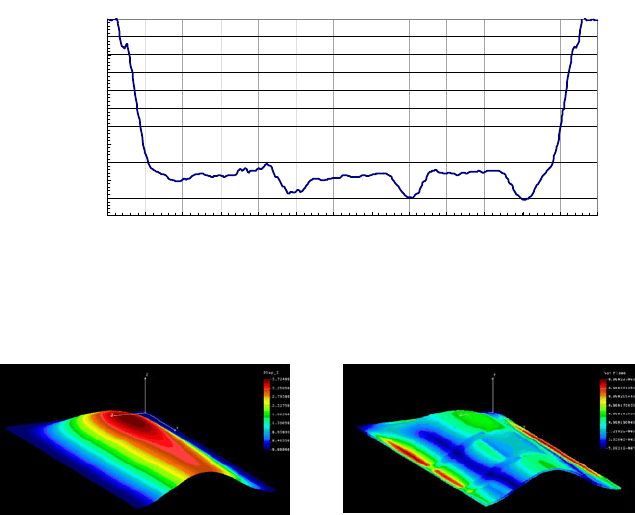
located at the bottom of the cavity, as can be seen from the fringe patterns. This is
also illustrated in Fig. 24 showing deformations measured along the longitudinal
line LL through the center of the diaphragm subjected to the HPS load of 100 psig,
for which the OELIM fringe pattern is displayed in Fig. 22f.
Examination of Fig. 23 shows that, because there is no mechanical stop on the
LPS, the diaphragm deforms without any obstructions reaching maximum
deformation/displacement of 3.458 μm at the LPS load of 100 psig (Fig. 23f).
This result is in good correlation with the maximum deformation/displacement of
3.724 μm determined computationally using the FEM model, Fig. 25;
representative von Mises stress field, based on the FEM half-model, is displayed
in Fig. 26.
-1.1
-1
-0.9
-0.8
-0.7
-0.6
-0.5
-0.4
-0.3
-0.2
-0.1
0
0 50 100 150 200 250 300 350 400 450 500 550 600 650
POSITION ALONG THE DIAPHRAGM, µm
DEFORMATION, µm
Fig. 24. Deformations of a DP diaphragm along the longitudinal line LL through the center
of a diaphragm, corresponding to the HPS load of 100 psig (see Fig. 22f).
Fig. 25. Representative 3D deformations of
a DP diaphragm subjected to the LPS load
of 100 psig, based on the FEM analysis,
half-model representation was used because
of the design symmetry of the sensor.
Fig. 26. Representative von Mises stress field
of a multilayer DP diaphragm subjected to
the pressure of +10 psig, based on the FEM
analysis, half-model representation was used
because of the design symmetry of the
sensor.
Recent Advances in Microelectromechanical Systems and Their Applications 267
Previous results, determined along the longitudinal lines through the center of
the diaphragm, indicate that the deformations at rest range from –20 nm to +90
nm, for the PPSs considered [40]. Furthermore, at the positive and the negative
differential pressures of the magnitude of 10 psig, these deformations are +813 nm
and –792 nm, respectively, i.e., they display a 21 nm difference, although
(according to the fundamental theories) they should be identical, i.e., the
difference should be 0. This data is essential for proper quantitative interpretation
of the signals produced by a MEMS PPS.
Using OELIM methodology, deformations of a PPS diaphragm can be
measured as a function of increments in pressure, both, along the longitudinal and
transverse lines, LL and TT, respectively, to facilitate their correlation [40].
FEM model of a MEMS PPS was developed in this study [40]. This model
incorporates the multilayer structure of a diaphragm and accounts for material
properties of each layer. It also incorporates the strain gages and their operational
characteristics. Because of the design symmetry of the sensor, half-model of the
diaphragm was used to facilitate/speed up the solution of cases considered.
The FEM model was used to determine response of a PPS to a variety of the
applied pressure and temperature conditions. It was also used to study the
structure of a diaphragm and the effects that the strain gauges have on its response
to the applied pressure and temperature loads [41]. Comparison of the
computational and experimental results on MEMS PPSs shows good correlation,
well within the uncertainty limits.
4.4 Deformations of a Cantilever Microcontact
MEMS RF switches present a promising technology for high-performance
reconfigurable microwave and millimeter wave circuits [42]. Low insertion loss,
high isolation, and excellent linearity provided by MEMS switches offer
significant improvements over an electrical performance provided by conventional
p-i-n diode and metal-oxide semiconductor field-effect transistor (MOSFET)
switching technologies. These superior electrical characteristics permit design of
MEMS switched high-frequency circuits not feasible with semiconductor
switches, such as high-efficiency broadband amplifiers and quasi-optic beam
steering arrays. In addition, operational benefits arise from low power
consumption, small size and weight, and integration capability of modern RF
MEMS switches.
Effective computational simulation of an RF MEMS switch must
simultaneously combine different loads including, but not limited to, the
following: electromagnetic, electrostatic, thermal, mechanical, and aeroelastic
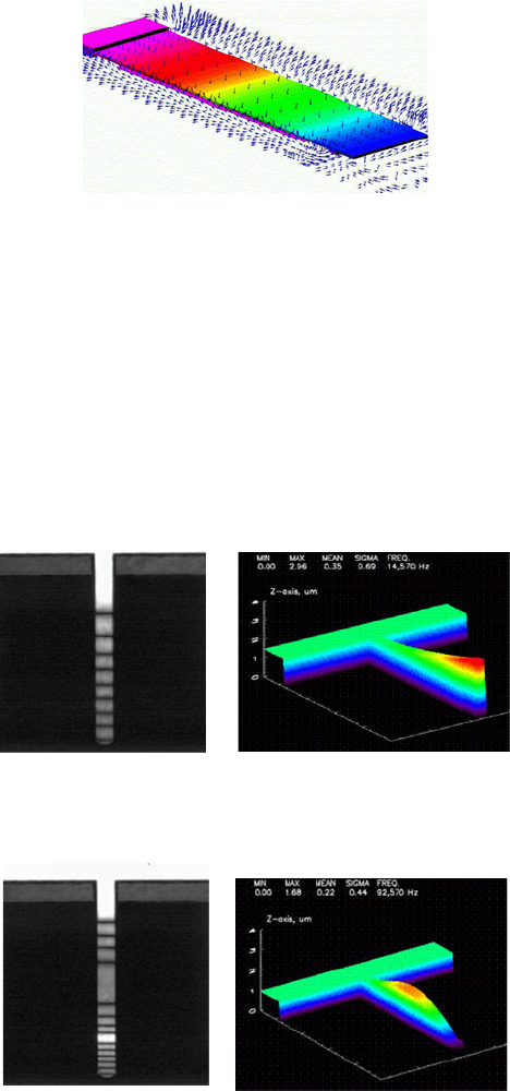
[19]. A representative result of such computational multiphysics modeling is
shown in Fig. 27, which indicates damping effects of air “surrounding” a
microswitch in its package.
In some applications, the damping effects displayed in Fig. 27 help control
switch dynamics and enhance tribological characteristics of the microcontacts; in
others, they adversely affect performance of the microcontacts [23].
268 R.J. Pryputniewicz
Fig. 27. Computational multiphysics simulation of an RF MEMS contact closure at
atmospheric conditions: 3D representation of air damping.
Prototype microcantilever beams were fabricated and their dynamic
characteristics were determined in real-time using optoelectronic methodology
[22]. For example, results were obtained for the 350 μm long microcantilevers.
Representative fringe patterns, corresponding to the first three flexure/bending
modes are shown in parts (a) displayed in Figs 28 to 30, respectively; these figures
exhibit maximum deformations ranging from about 3 μm down to 870 nm as
frequency increases from 14.57 kHz to 261.4 kHz; however using different
samples deformations of picometer (pm) magnitudes were recorded in a previous
study [24].
Fig. 28. OELIM measurements of a vibrating MEMS cantilever – resonating at 14,570 Hz
corresponding to the first flexure mode: (a) time-average fringe pattern, (b) mode shape
based on the fringe pattern of part (a) exhibiting maximum deformation of 2.96 μm.
Fig. 29. OELIM measurements of a vibrating MEMS cantilever – resonating at 92,570 Hz
corresponding to the second flexure mode: (a) time-average fringe pattern, (b) mode shape
based on the fringe pattern of part (a) exhibiting maximum deformation of 1.68 μm.
(b)
(a)
(b)
(a)
