Hawkes P.W., Spence J.C.H. (Eds.) Science of Microscopy. V.1 and 2
Подождите немного. Документ загружается.


Chapter 6 In Situ Transmission Electron Microscopy 465
A
B
Figure 6–10. Deposition of Au on Si observed by
different in situ imaging modes. (A) Step bunching
on vicinal Si(001). A series of REM images obtained
during the deposition of Au at 800°C onto a vicinal
(4° miscut) Si(001) surface shows fi rst the forma-
tion of (001) terraces in (a) and (b). Step bunching
and formation of step bands are shown in (c) and
(d); facet nucleation on the step bands in shown in
(f) and (g). Finally there is a complete transforma-
tion of the entire vicinal surface into a hill-and-
valley structure of (001) superterraces and (119)
and (117) facets (h). (From Minoda et al., 1999 with
kind permission of Taylor and Francis Ltd.) (B) The
Au-induced reconstruction of a fl at Si(001) surface
on heating. The sample was prepared by deposit-
ing Au onto a rough, oxidized Si particle. The
irregular sample geometry means that the tem-
perature is not accurately known, However, on
heating, the Au fi rst agglomerated; further heating
caused the oxide layer to disappear and the Au to
spread over the surface (dark line along the sample
edge), causing localized faceting into (001) and
other terraces. The (001) facets then reconstruct
over the timeframe shown, starting from the
terrace boundary (arrows A and B). (Reprinted
with permission from Kamino et al., © 1997 by the
American Physical Society.)

466 F.M. Ross
Surface diffusion under beam irradiation is evident during profi le
imaging. This has been used to advantage to study narrow wires in
situ. Two adjacent holes are formed in a thin foil and the neck between
them observed as it thins and breaks due to inbuilt stresses. Such
experiments show a variety of interesting non-bulklike structures in
Au (Figure 6–11), such as single chains (Koizumi et al., 2001) and helical
multishell wires (Kondo and Takayanagi, 2000; Oshima et al., 2003a),
with some of the structures related to shear (Oshima et al., 2003b).
Beam-induced atom migration reduces the dimensions one layer at a
time (Oshima et al., 2002). Unusual wire structures also form in Pt
(Oshima et al., 2002). The surface diffusion of single atoms, for example
W on MgO, can be imaged in TEM (N. Tanaka et al., 1998).
Controlled environment and UHV TEM thus has an excellent track
record for creating and observing surface reconstructions and observ-
ing step motion and surface diffusion. We now focus on some specifi c
applications where the ability to characterize and modify surfaces in
situ has led to particularly interesting and signifi cant advances.
3.2 Catalysis
Controlled environment TEM has enabled pioneering studies of the
structural details of reactions during heterogeneous catalysis (Gai,
2002a; Sharma, 2001, 2005). High resolution imaging can be carried out
at high temperature and under a controlled gas environment, up to
several millibar of, say, H
2
, CO, or O
2
. Catalyst surface structure has
been related to reactivity, intermediate phases have been determined,
and changes in catalyst structure have been visualized during activa-
tion and poisoning. Several controlled environment TEMs are in opera-
Figure 6–11. Nano-
structures formed by
surface mobility.
Images of stable Au
nanowires observed
during the electron
beam thinning of a
specimen. The diame-
ters of the wires are
(A–D) 1.3, 1.1, 0.8, and
0.6 nm, respectively.
The wire images are
wavy, especially the
thinnest, and can be
modeled with helical
structures. (Reprinted
with permission from
Kondo and Takaya-
nagi, © 2000, AAAS.)
Chapter 6 In Situ Transmission Electron Microscopy 467
tion in industrial laboratories, and we suspect that the many important
results remain proprietary!
Most studies have focused on catalysts consisting of metal particles
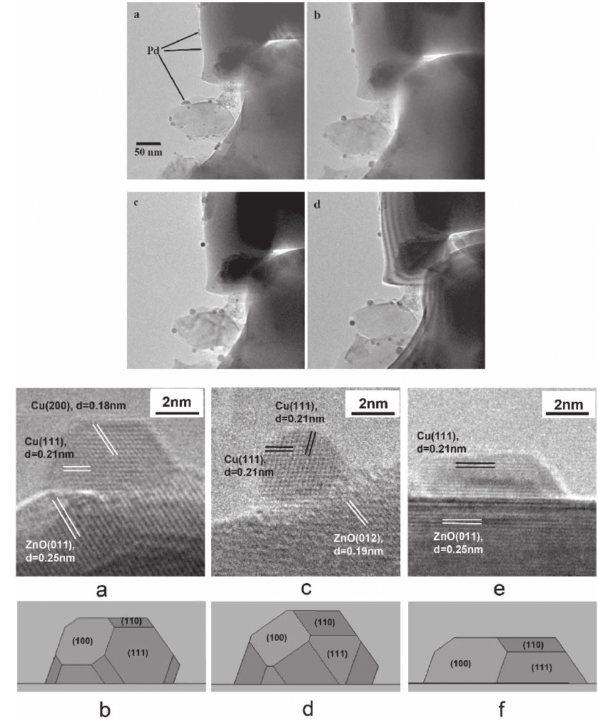
on an oxide substrate (Figure 6–12). Gai et al. (1990) fi rst examined
shape changes in Cu particles in oxidizing and reducing environments,
and observed the stability of Pt and Ru particles on TiO
2
(Gai 1998; Gai
et al., 2000). Hansen et al. examined the effect of Ba promoters on
surface structures in Ru particles (2001), and used the shapes of Cu
particles to determine relative surface energies under oxidizing and
reducing conditions (2002; Figure 6–12B). Regeneration processes are
important in such catalysts, and here too in situ studies have proven
useful. For example, during regeneration of Pd/Al
2
O
3
catalyst, sinter-
ing also takes place. The sintering behavior of “used” Pd particles,
studied using analytical TEM as well as controlled environment
heating, is affected by hydrocarbons which build up during use of the
catalyst (R.-J. Liu et al., 2004; Figure 6–12A).
A wide variety of other materials and reactions have also been inves-
tigated under a controlled environment. Gai and Kourtakis (1995)
observed a glide shear rearrangement in vanadium pyrophosphate
during reduction, and developed a model for the surface activity of
this material, which is important in butane catalysis. Sharma et al.
(2004a) examined structural changes during reduction of CeO
2
cata-
lyst, and interestingly used in situ energy loss spectroscopy to deter-
mine oxidation states as a function of temperature. Even the growth of
polymeric reaction products in situ has been observed (Crozier et al.,
2001; Gai, 2002b). Other reactions include intercalation in some inter-
esting layered structures (Diebolt et al., 1995; Sidorov et al., 1998b), the
nitridation of zirconia (Sharma et al., 2001), and de- and rehydroxyl-
ation of the lamellar material Mg(OH)
2
, which is important in CO
2
sequestration (McKelvy et al., 2001). The reaction of MgO with water
vapor has also been observed in situ (Sharma et al., 2004b; Gajdardziska-
Josifovka et al., 2005).
Finally, photocatalysis can be studied in situ if a UV light source is
brought into the specimen area. High resolution in situ imaging of the
decomposition of hydrocarbons deposited on a TiO
2
fi lm (Yoshida et
al., 2005) provides information on the mechanism of the process. These
exciting results suggest that in situ studies will continue to have an
important impact in the future development of catalysts and other
functional materials.
3.3 Oxidation of Surfaces
Corrosion of metals has signifi cant impact on industry, so it is impor-
tant to gain a fundamental understanding of oxidation and reduction
by comparing controlled observations with theoretical predictions. For
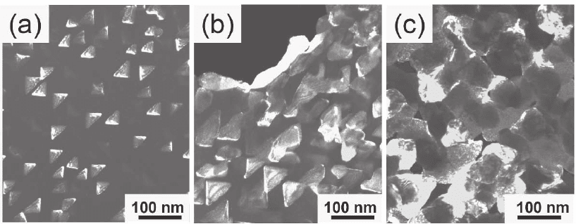
copper, oxidation was found to proceed via nucleation, growth, and
coalescence of oxide islands (Figure 6–13). This result allowed the
development of oxidation theories beyond simple models that had
assumed a continuous oxide fi lm (Yang et al., 1998, 2002; Zhou and
Yang, 2002, 2003). Other than Cu and its alloys (Wang and Yang, 2005),
468 F.M. Ross
A
B
Figure 6–12. In situ imaging of catalysts. (A) Fresh Pd/A l
2
O
3
catalyst (used for hydrogenation of acety-
lene) (a) in the as-received condition (room temperature), and (b–d) after heating in 500 m Torr steam
at 700ºC for 1, 4, and 7 hours. Catalysts are regenerated by heating in steam to remove hydrocarbon
buildup, but this causes sintering of the metal particles, reducing activity. In situ experiments show
that, for fresh catalysts, sintering is by conventional Ostwald ripening, while movement and coales-
cence occurs for used catalysts. (Reprinted with permission from R.-J. Liu et al., © 2004 AAAS.) (B)
Images of a Cu/ZnO catalyst (the methanol synthesis catalyst) in various environments at 220ºC,
together with the corresponding Wulff constructions of the Cu nanocrystals. (a, b) 1.5 mbar H
2
at 220ºC;
(c, d) in a mixture of H
2
and H
2
O with ratio 3 : 1 at a total pressure of 1.5 mbar; (e, f) in a mixture of
95% H
2
, 5% CO at a total pressure of 5 mbar. These images allow the relative surface energies to be
determined as a function of environment. (From Hansen et al., © 2002. Courtesy of Cambridge Uni-
versity Press.)
Chapter 6 In Situ Transmission Electron Microscopy 469
metal oxidation remains largely unstudied, but in situ experiments
could clearly offer the possibility of improving corrosion resistance
through alloying or surface processing.
Silicon oxidation is another industrially signifi cant process, as a
defect-free Si/SiO
2
interface is fundamental to transistor operation. For
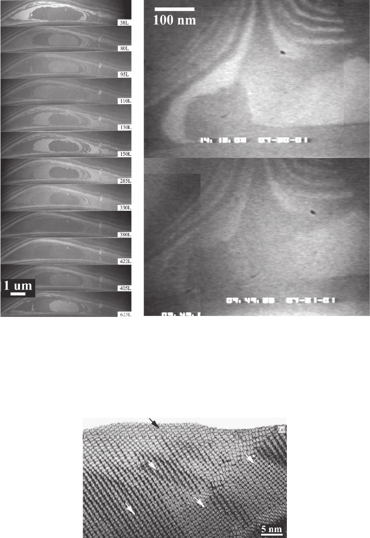
Si(111) (Figure 6–14A), forbidden-refl ection imaging showed that steps
do not move during oxidation, meaning that any surface roughness
remains during processing (Ross and Gibson, 1991; Ross et al., 1994b).
For Si(001), the same result is seen (Figure 6–14B). Forbidden refl ection
experiments are useful in their ability to probe the buried Si/SiO
2
interface, and are complementary to results obtained by in situ scan-
ning refl ection electron microscopy (Ichikawa, 1999).
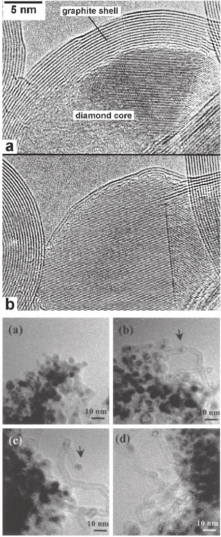
High resolution imaging provides insights into reactions in more
complex materials. By oxidizing and reducing niobium oxides, Say-
agues and Hutchison (1996, 2002) showed the formation of a series of
block structures with changing stoichiometry (Figure 6–15). The com-
bination of analytical techniques with imaging would undoubtedly
lead to further useful insights into oxidation and related reactions.
3.4 Growth of Carbon Nanostructures
The growth of carbon nanostructures has been extensively studied in
situ since the discovery of these interesting materials by TEM. It is rela-
tively easy to form carbon structures in situ with a controlled environ-
ment plus a catalyst or a graphitic precursor (Figure 6–16). Beam effects
provide an important ingredient in the synthesis, especially if catalysts
are not used. The beam interacts with the atmosphere above the speci-
men producing a plasma that can generate fullerenes (Burden and
Hutchison, 1998). Alternatively, irradiation of graphitic materials
Figure 6–13. Mechanism of copper oxidation. Dark-fi eld images obtained during oxidation of Cu at
0.1 Torr and 350°C in a UHV TEM. Imaging using the Cu
2
O {110} refl ection showed that oxidation is
not planar, but takes place by Cu
2
O island (a) nucleation (5 min), (b) growth (15 min), and (c) coales-
cence (25 min). The specimen was prepared by fl oating a 60-nm Cu fi lm onto a support and then
removing the surface oxide in situ by annealing at 350°C in methanol vapor for 15–30 min. The area
and number density of the islands grown both at low pressure and at high pressure (shown here)
were modeled using Johnson–Mehl–Avrami–Kolmogorov theory to give surface diffusion parameters.
(Reprinted with permission from Yang et al., © 2002. American Institute of Physics.)
470 F.M. Ross
A
B
Figure 6–14. Mechanism of silicon oxidation. (A) Series of images of an Si(111) sample observed in
plan view during oxidation in 2 × 10
−6
Torr water vapor at 400°C. The time of each frame is given. A
1/3 (422) forbidden refl ection was used to form the images so that the gray levels correspond to ter-
races, with intensities repeating every unit cell (three steps). Steps do not move during oxidation of
several layers showing that step sites are no more reactive than terrace sites. (Reprinted with permis-
sion from Ross and Gibson, © 1991 by the American Plysical Society.) (B) Two images of an Si(001)
sample observed before and after oxidation in air at room temperature. A 1/4 (220) forbidden refl ec-
tion was used to form these images. The steps do not move on this surface either.
Figure 6–15. Oxidation of a block oxide structure. High-resolution image of an Nb
22
O
54
crystal after
heating by the electron beam and exposure to 15 mbar oxygen. The partly oxidized structure consists
of microdomains of Nb
10
O
25
(arrowed) in an Nb
22
O
54
matrix. These images have been used to identify
the structure of the Nb
10
O
25
phase and the complete oxidation sequence from Nb
12
O
29
to Nb
10
O
25
has
been determined using in situ experiments. (From Sayagues and Hutchison, 2002 with permission
from Elsevier.)
Chapter 6 In Situ Transmission Electron Microscopy 471
A
B
Figure 6–16. Carbon nanostructure
growth in situ. (A) For mation of diamond
in situ. Poly hedral graphitic particles
were produced by arc-discharge and
were transformed into perfectly spheri-
cal onions by electron beam irradiation
above 600K. The decreasing distance
between shells toward the center showed
that the onions are in a state of high self-
compression. The nucleation of cubic
diamond occurs in the centers of the
onions during irradiation above 900K,
and the diamond grows until, surpris-
ingly, almost all the onion shells are con-
sumed. (a) After 2 h of irradiation at
1.25 MeV and 20 mA cm
−2
. (b) After a
further hour of irradiation. A typical
twin is visible in the diamond. High
pressure appears necessary to nucleate
the diamond, but further growth is by
beam-induced defects. (Reprinted with
Permission from Banhart, © 1997. Amer-
ican Institute of Physics.) (B) Growth of
multiwalled carbon nanotubes by cata-
lytic chemical vapor deposition. Bright-
fi eld images showing an Ni-SiO
2
catalyst
(a) exposed to H
2
at 450°C; (b) after
exposure to acetylene (300 mTorr of an
H
2
–C
2
H
2
mixture), and (d) another part
of the sample after 3 min. The arrows
show an individual Ni particle. At higher
temperatures single-walled tubes
formed but with catalysts present at the
bases rather than the tips of the tubes.
(Reprinted with permission from
Sharma and Iqbal, © 2004. American
Institute of Physics.)
472 F.M. Ross
generates point defects which deform the graphitic sheets, forming
new structures (Ugarte, 1992; Banhart, 1997), while irradiation of mate-
rials such as Cu implanted with C causes graphitic onions to grow (Abe
et al., 2002). Familiar or new C and BN structures, and even formation
of diamond from graphite, can thus be observed in situ (Ugarte, 1992;
Ru et al., 1996; Niihara et al., 1996; Banhart, 1997, 1999, 2003; Bengu and
Marks, 2000; Roddatis et al., 2002; Troiani et al., 2003; Gloter et al., 2004;
Wang et al., 2005).
Carbon nanotubes are of particular interest, and can be grown in situ
by introducing a precursor gas such as methane, propylene, or acety-
lene over a catalyst (Sharma and Iqbal, 2004; Sharma et al., 2005).
During growth, individual catalyst particles change their shape, and
nucleation sites can be identifi ed (Helveg et al., 2004). Once grown,
carbon nanotubes can be modifi ed with the beam (Terrones et al., 2000,
2002) to produce more complex structures.
3.5 Epitaxial and Polycrystalline Thin Film Growth
The experiments in Section 3.4 have shown the exciting possibilities
for controlled environment growth of nanostructures. Continuous thin
fi lms can also be grown in situ, and this allows important processes
such as nucleation, development of surface morphology, and relaxation
to be observed. Although some studies describe polycrystalline fi lm
growth (for example Al; Drucker et al., 1995), most systems examined
in situ have been epitaxial. These include Au on MgO (Kizuka and
Tanaka, 1997a, b), Ge on Si (see below), and silicides on Si (Section 2).
These experiments can provide detailed and quantitative information
if growth conditions such as fl ux and temperature are calibrated
carefully.
The most detailed studies have examined Ge and SiGe epitaxy on
Si. This is a “test system” for studying epitaxial growth phenomena
which also has great relevance to the development of microelectronic
devices. A true UHV environment is required for the experiments, as
the Si substrate foil is cleaned by heating in UHV to above the oxide
desorption temperature. Growth is then carried out by UHV-CVD
using gases such as disilane or digermane. Growth was observed by
Krishnamurthy et al. (1991) in STEM, and by Minoda and Yagi (1996)
and Ichikawa et al. (1998) in REM. But most work in this system has
been carried out using conventional weak beam imaging in plan view,
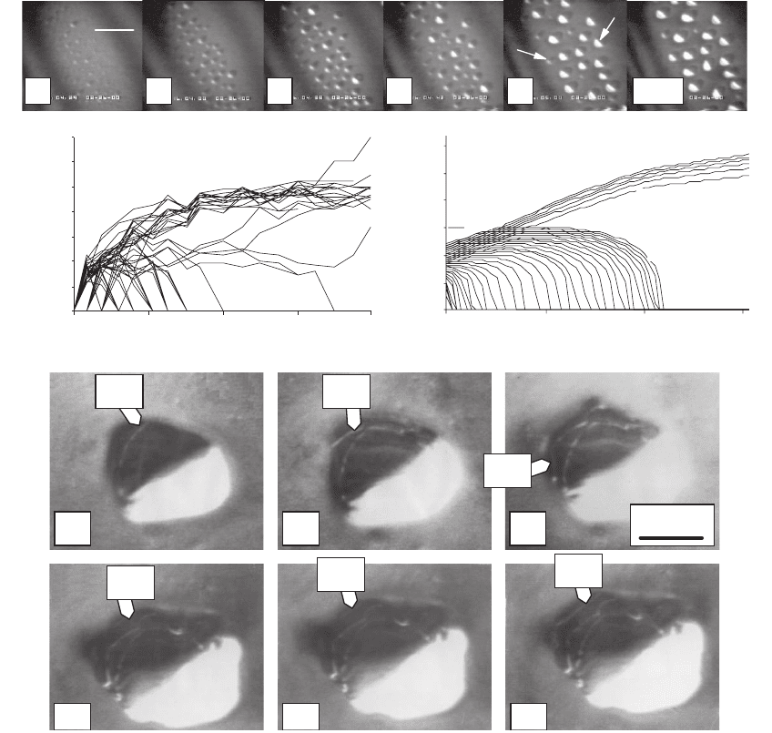
giving the highest sensitivity to strain fi elds (Figure 6–17). LeGoues et
al. (1996) and Hammar et al. (1996) grew Ge on Si(111) and (001) in situ,
clearly imaging the initial surface reconstruction, the nucleation of Ge
islands, and later their growth and coalescence. The structures pro-
duced depend strongly on growth conditions. By varying the parame-
ters, a range of fascinating phenomena now known to be common in
other epitaxial systems was observed, such as the change in island
shape during the introduction of stress-relieving dislocations (LeGoues
et al., 1994, 1995). The range of structures observed in these studies
would have been tedious to capture ex situ, and dynamic phenomena
Chapter 6 In Situ Transmission Electron Microscopy 473
0.0
020406080
0
10
20
30
40
50
60
70
0102030
0.0
0.5
1.0
1.5
2.0
2.5
3.0
V
1
S
L
04
Is
Tim e (seconds)
V
C
Time (seconds) Time step
200nm
34
3 7
12
16
50 sec
P
D
a c
d f
b
e
D2
D3
D2
D3
D3
D1
50nm
P
D
Island diameter (nm)
Island size
A
B
D
C
Figure 6–17. Ge island nucleation, growth, and relaxation. (A) Island coarsening. A series of video
frames showing stages of island growth within a 0.5 µm × 0.5 µm area. Growth conditions were 5 ×
10
−7
Torr Ge
2
H
6
and 650°C. Weak beam images were acquired in a (g, 3g) condition with g = 220. The
time of each frame after “nucleation” (fi rst appearance of islands) is given. (B) The time evolution of
every island within the area. (C) A simulation showing the fate of islands with different initial sizes,
based on a modifi ed Ostwald ripening process in which islands coarsen but also undergo a shape
transition at V
c
. The scale of the plot is chosen to match the data shown in (b). (Reprinted with permis-
sion from Ross et al., © 1998 by the American Physical Society.) (D) The introduction of dislocations
into a partially relaxed island. Images were obtained 59, 94, 96, and 140 min after the beginning of
growth, with the last three images taken within 1 s of each other. Growth conditions were 650°C and
10
−6
Torr of 10 : 1 He : GeH
4
. Only dislocations in the dark part of the image can be seen (D1–D3). (From
Hammar et al., 1996 with permission from Elsevier.)
such as island shape changes and the essential role of Ostwald
ripening (Ross et al., 1998) would not have been detected without the
use of in situ TEM. Changes caused by the presence of surfactants
during growth have also been examined in situ (Maruno et al., 1996;
474 F.M. Ross
Portavoce et al., 2004). It is interesting to note that complementary
studies using in situ LEEM have been important in fully understanding
growth in the SiGe system, as LEEM is more sensitive to surface struc-
ture (e.g., Ross et al., 1999b).
When low Ge content (say 15%) SiGe is grown on Si, islands are not
seen, but instead a continuous fl at layer forms. When suffi ciently thick,
this fi lm relaxes by introduction of dislocations. The motion of these
dislocations can be measured during fi lm deposition and compared
with dislocation dynamics during post-growth annealing, which will
be discussed in Section 5. Interestingly, the parameters governing dis-
location motion are different during growth, where the surface is H
terminated, versus during annealing, where the surface is oxidized
(Stach et al., 1998b, 2000). A higher kink nucleation rate under the oxi-
dized surface, perhaps due to surface stress or increased point defects,
is the probable cause. This is important for modeling relaxation during
device processing, and shows once again the unique information that
can be obtained when materials are observed during growth rather
than ex situ.
3.6 Crystal Growth on Patterned Surfaces
An interesting extension of the growth studies described above is the
study of crystal growth on a non-uniform substrate. By carrying out
growth on substrates which have been patterned to create areas of dif-
ferent reactivity, strain, or topographic contrast, the effect of these
parameters on growth may be visualized directly and even quantita-
tively, if kinetic data is obtained.
Again, most work has been done in the SiGe system, motivated by
an interest in controlling island self-assembly for fabricating novel
electronic devices. It is well known that if Ge is deposited on patterned
Si, islands form at positions aligned with the topography. In situ mea-
surement of nucleation times at different locations (Ross et al., 2004)
showed that this is controlled by competition between edge adsorption
of adatoms and terrace nucleation. Patterns may also be created with
a focused ion beam. At low doses, this forms a shallow topography
(Figure 6–18A) that is suffi cient to control nucleation and alter wetting
layer thickness (Kammler et al., 2003; Portavoce et al., 2006). In these
experiments the focused ion beam gun was installed in a chamber
connected to the TEM by UHV. The inclusion of surface processing
tools that are not in situ (i.e., in the polepiece) but are within the
microscope’s vacuum system enables a wider range of processes to be
carried out controllably.
A second example also relates to semiconductor nanostructures:
vapor-liquid solid growth of nanowires. Here, a droplet of liquid eutec-
tic catalyzes growth to form elongated wirelike structures. This process
has been imaged in situ in plan view, allowing wire growth to be
observed qualitatively, in Si/Au (Wu and Yang, 2001), Si/Fe (Zhou et
al., 2002), and GaN (Stach et al., 2003). In GaAs/Au (Persson et al.,
2004), post-growth heating of wires was used to deduce an alternative
mechanism, vapor-solid-solid growth. If experiments are performed in
