Hawkes P.W., Spence J.C.H. (Eds.) Science of Microscopy. V.1 and 2
Подождите немного. Документ загружается.

Chapter 6 In Situ Transmission Electron Microscopy 495
Activation energies and prefactors were measured for dislocation
nucleation and propagation. Note that a well calibrated system is neces-
sary if TEM-derived parameters such as activation energy are to be
meaningful. In this case, the sample temperature was calibrated using
Si regrowth (Section 2.1.1), and fi nite element analysis was used to
determine the conditions under which sample bending could be
neglected (Hull and Bean, 1994). The parameters determined in situ
were eventually used in a processing model for microelectronic device
design (Hull et al., 1989).
A similar experimental approach allows other features of the relax-
ation process to be examined as well. Dislocation nucleation has been
studied in SiGe/Si implanted with F (Stach et al., 1998a) and with He,
which forms platelets and bubbles (Follstaedt et al., 1997; Hueging et
al., 2005). Although most work has been in the SiGe/Si system, a few
other epitaxial systems have been studied as well, such as BaTiO
3
on
SrTiO
3
(Sun et al., 2004), ZnSe on GaAs (Lavagne et al., 2001), and Al
on Al
2
O
3
(Dehm et al., 2002). Clearly, many other materials systems
could yield useful information with this technique.
We fi nally note that dislocation confi gurations in thin fi lms, such as
in Figure 6–27A, are somewhat random. However, in well controlled
geometries—relaxed epitaxial islands, or surfaces with modulated
stress fi elds—dislocation locations can be predicted accurately (Liu et
al., 2000; Kammler et al., 2005). This suggests opportunities for in situ
TEM to provide quantitative information on dislocation nucleation and
growth in fi nite nanostructures with built in strain, such as epitaxial
islands or composite wires or ribbons.
5.3 Mechanical Properties of Nanostructures, Thin Films,
and Surfaces
TEM is particularly appropriate for studying the mechanical properties
of small volumes of material. In the work discussed so far, the same
stimulus (strain, heat) is applied to the entire specimen. By applying
the stimulus to only a small part of the specimen, the correlation
between mechanical input and structural response can hopefully be
made more precise. In this section we discuss experiments in which
small volumes of a specimen are mechanically deformed (nanoinden-
tation), the surface is probed, or nanostructures are deformed. These
experiments make use of scanning probe techniques to bring a tip near
the sample for controlled deformation of an area under observation.
5.3.1 In Situ Indentation of Thin Films
By integrating a nanoindenter into a specimen holder, it is possible to
examine localized deformation of single crystals, polycrystalline mate-
rials, and layered structures. Nanoindentation holders have been
described by Wall and Dahmen (1998), Stach et al. (2001), Minor et al.
(2001), Bobji et al. (2003) and Ii et al. (2004). The design must include
some way of making sure the indent occurs in an electron transparent
region of the specimen. In the design of Wall and Dahmen, for example,
a Si sample (mounted vertically) is etched to form a ridge which proj-
ects out into the beam. Elastic deformation followed by dislocation
496 F.M. Ross
formation is visible in this ridge during indentation. Using this sample
geometry, the motion of dislocations and grain boundaries under the
indenter tip has been studied in a variety of materials deposited onto
the substrate. In ultra fi ne grained Al, for example, grain boundary
motion occurs under the tip (Jin et al., 2004). This does not occur in
Al-Mg, suggesting that solute drag is important (Soer et al., 2004).
Similarly, in Ni, deformation proceeds by diffusion-controlled grain
boundary-mediated processes rather than dislocation motion within
grains (Shan et al., 2004). Si shows dislocation plasticity on room tem-
perature nanoindentation (Minor et al., 2005). Nanoindentation of mar-
tensitic steel is shown in Figure 6–28 (Ohmura et al., 2004), and the
formation of dislocations and the strain transfer across grain boundar-
ies are visible. As well as dislocation formation and motion, nanoin-
dentation can cause crack propagation. The nature and pathway for
such cracks can be determined (Ii et al., 2004; Matsunaga et al., 2004).
In the future, we expect to see exciting developments in the area of in
situ nanoindentation, driven by the incorporation of sensors that allow
stress-strain curves to be measured during deformation. This suggests
exciting possibilities for quantitative analysis of nanoscale mechanical
properties.
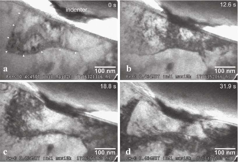
Figure 6–28. Nanoindentation of steel. Series of images of an Fe-C martensite, including a low-angle
grain boundary. (a) Before indentation, (b) at 21 nm penetration depth, showing dislocation emission
beneath the indenter, (c) at 46 nm penetration depth, showing dislocation pileup at the grain boundary,
and (d) at 84 nm penetration depth, demonstrating dislocation emission at the far side of the grain
boundary. (From Ohmura et al., ©2004. Courtesy of Institute of Materials Research Society.)
Chapter 6 In Situ Transmission Electron Microscopy 497
5.3.2 Tribology and Nanomanipulation
Nanoindentation is only one of several interesting experiments that
can be carried out in holders incorporating a scanning tip with piezo-
electric actuators. For example, the tip can be used for fundamental
studies of tribology by scraping it across a surface. Tip-substrate inter-
actions were observed in refl ection mode geometry as a graphite speci-
men was imaged using STM (Spence et al., 1990; Lo and Spence, 1992),
and changes in the surface were attributed to shearing and abrasion.
Using a similar holder in a UHV TEM, Naitoh et al. (2000) correlated
the atomic confi guration at a tip surface with the resolution of STM
images it produced. Fujisawa and Kizuka (2003a) and Ohnishi et al.
(1998a) observed the motion of a tip across a stepped surface and deter-
mined the effects of rastering and surface topography on lateral dis-
placement. This sort of i n f o r m at io n i s n at u r a l l y important in interpreting
scanning probe images.
Alternatively, an in situ STM tip can be used to form small necks or
grain boundaries by touching it to the surface, deforming both materi-
als (Figure 6–29). The structure of these necks can then be observed at
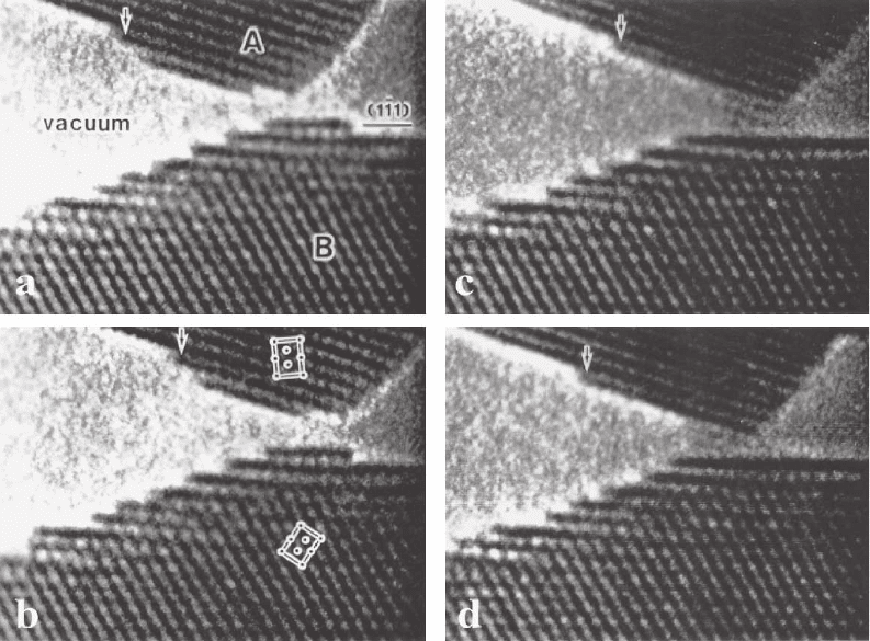
Figure 6–29. STM surface manipulation. Series of high-resolution images of atomic-scale removal type
mechanical processing of an Au surface. A region six atomic columns wide on the fi xed side (B) is
removed by the Au tip on the mobile side (A). On both sides the beam is parallel to the [110] axis. The
time is (a) 0 s, (b) 1.2 s, (c) 3.5 s, and (d) 5.8 s. Boxed circles show the unit cell of Au. These images give
a visual impression of events that may occur during STM operation as well as phenomena associated
with friction. (From Kizuka et al., © 1998c. Courtesy of Cambridge University Press.)
498 F.M. Ross
high resolution. Kizuka and Hosoki (1999) recorded the interactions as
two oxidized Si tips came into contact, observing the strength of the
boundaries formed, and Naitoh et al. (2000) observed twins in necks
of Si formed between clean Si and a W tip. Most work, however, has
involved Au. Kizuka (1998a, b) showed formation of a neck between
Au contacts and observed compression, shear, deformation, slip, and
twinning. These videos give a stunning visual impression of the inter-
action of the tip with a surface during scanning, and allow a study of
friction at the nanoscale (Fujisawa and Kizuka, 2003b). Naturally, the
electrical properties of such necks can also be studied, and this will be
described in Section 6.
5.3.3 Mechanical Properties of Nanostructures
The mechanical properties of elongated nanostructures are a natural
subject for in situ studies. For carbon nanotubes, mechanical parame-
ters such as Young’s modulus were fi rst measured by observing the
vibration of tubes which extend out as cantilevers (Krishnan et al.,
1998). These tubes vibrate because of coupling to motion in the stage.
However, the mechanical properties of tubes can also be measured by
bending them with an STM tip. Individual CNTs can be bent and
broken (Kuzumaki et al., 2001) and stress and strain can be measured
during deformation (Asaka and Kizuka, 2005). The welding of CNTs
to a tip can be seen (Hirayama et al., 2001; Kuzumaki et al., 2004). A
tip can even be used to operate a bearing made of telescoping CNTs
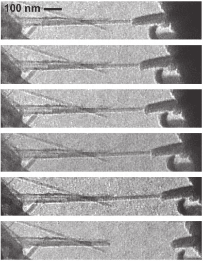
(Cumings and Zettl, 2000; Figure 6–30). Such experiments can use the
Figure 6–30. Mechanical properties of a
carbon nanotube. Selected frames of a video
recording of the in situ telescoping of a multi-
walled nanotube. In the fi rst fi ve frames, the
core nanotubes are slowly withdrawn to the
right. In the sixth image, which occurred one
video frame after the core was released, the
core has fully retracted into the outer nanotube
housing as a result of the attractive van der
Waals force. (Reprinted with permission from
Cumings and Zettl, © 2000, AAAS.)
Chapter 6 In Situ Transmission Electron Microscopy 499
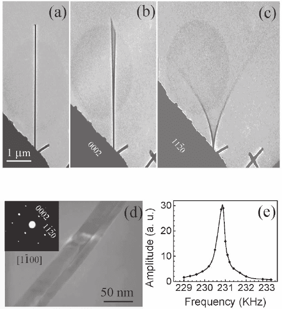
Figure 6–31. Mechanical properties of a nanobelt. A ZnO nanobelt at (a) stationary, (b) the fi rst-har-
monic resonance in the x direction, frequency 622 kHz, and (c) the fi rst- harmonic resonance in the y
direction, frequency 691 kHz. (d) An enlarged image of the nanobelt and its electron diffraction pattern
(inset). The projected shape of the nanobelt is apparent. (e) The FWHM of the resonance peak mea-
sured from another ZnO nanobelt. The resonance occurs at 230.9 kHz. (Reprinted with permission
from Bai et al., © 2003. American Institute of Physics.)
TEM for more than just imaging; for example, Suenaga et al. (2001)
were able, using EELS, to probe changes in electronic structure during
bending of multiwalled and bundled single walled CNTs, and correlate
these changes with deformation.
By using a stage with piezo drives to induce an alternating electrical
fi eld between a nanowire and an electrode, controlled frequency vibra-
tions can be set up in the nanowire (Wang et al., 2001, 2002a). For
example, in ZnO wires of rectangular cross section, each direction of
vibration has its own resonances from which the modulus and time
constant or Q factor can be derived (Bai et al., 2003a; Figure 6–31). Such
measurements of bending modulus can be related to defects in indi-
vidual structures (Gao et al., 2000). In fact, the mechanical resonance
depends so sensitively on the structure that modulus measurements
have potential use for measuring small masses. A less quantitative
application (at present) is a stage developed for stretching chains of
nanoparticles, of interest for their use as reinforcing fi llers and their
500 F.M. Ross
presence in diesel exhausts (Suh et al., 2004). It will be exciting to see
these mechanical techniques applied to more complex structures such
as composite nanowires or fi lled CNTs.
5.4 Summary
Mechanical deformation has been successfully examined in situ using
several innovative techniques. The future challenge in mechanical
testing is to make its results even more quantitative and to minimize
or account for thin foil effects. Customised design of specimens using
MEMS technology, integrating for example tensile testers, tweezers,
notches, or other structures, will certainly become more widespread
for thin fi lm experiments. Measurement of stress-strain curves during
nanoindentation will provide accurate information on the mechanical
response of a system, for example as single dislocations are introduced.
Deposition of a fi lm of interest, perhaps with an engineered boundary,
onto a crystalline membrane may become useful in some cases, since
the substrate deformation can be measured accurately from its strain
contrast. Integration of such experiments with controlled atmosphere
TEM will allow materials to be tested under the most realistic condi-
tions. Elegant results on nanostructures have already been achieved
using nanomanipulation with a tip. There is no doubt that these types
of experiments are already bringing our understanding of the mechan-
ical properties of small volumes of materials to a new level of
precision.
6 Correlation of Structural and Electrical Properties
of Materials
We have shown that fascinating data can result from the correlation
between an applied stimulus, such as temperature, environment, or
strain, and a microstructural change. Extending this approach, if we
measure the electrical properties of a material while also observing or
changing its structure, we can investigate structure-electrical property
relationships in a unique way. The material under study can have a
large volume, perhaps most or all of the TEM sample. Alternatively,
structure-property relationships can be derived for individual
nanostructures.
These interesting experiments all require electrical biasing holders,
but not necessarily video rate recording, since the sample itself may
change only slowly, or not at all. Examples include measuring the con-
ductivity of individual nanowires as a function of their diameter, mea-
suring changes in resistance as voids form during electromigration,
measuring the potential distribution across p-n junctions as a function
of bias, or measuring conductivity after dislocations are introduced.
6.1 Electrical Measurements on TEM Samples: Complete Samples
as Devices
Many important processes can be studied by applying a voltage across
a bulk or patterned specimen in situ. We have already described the
Chapter 6 In Situ Transmission Electron Microscopy 501
use of an applied voltage to generate an electric fi eld for ferroelectric
switching (Section 4.3), and now consider other possibilities. One inter-
esting example is the measurement of electric fi elds across p-n junc-
tions. This has been a favorite topic from the early days (Darlington
and Valdre, 1975). More recently, a varying bias has been applied in
situ across a FIB-prepared p-n junction, using holography to measure
the potential distribution (Twitchett et al., 2002, 2004). The eventual
aim of such studies is to understand the complex fi elds within real
transistors, although quantitative image matching shows that surface
effects must fi rst be understood. Similar biasing experiments can be
useful probes of other materials too. For example, the potential distri-
bution across the boundary in a ferroelectric bicrystal was mapped by
holography (Johnson and Dravid, 1999, 2000), showing breakdown and
the presence of trap states associated with dopants.
In situ biasing also allows resistivity to be measured, which can then
be correlated with a structural transformation. Thus, the amorphous
to crystalline transformation for phase-change memory materials
(Section 2.1) can be correlated with resistivity, as shown in Figure 6–
32A (Verheijen et al., 2004). Similarly, phase transformations in TiNi
shape memory alloys can be related to resistivity (Ma and Komvopou-
los, 2005). Another interesting application of in situ resistivity measure-
ment is the observation of conductivity changes during ion or electron
beam irradiation to determine the cross section and threshhold energy
for Frenkel pair production (King et al., 1981; Haga et al., 1986).
In situ resistivity measurements have also been used to probe the
electrical properties of dislocations (Ross et al., 1993). In this experi-
ment, dislocations are formed progressively in a p-n junction diode by
heating a metastable SiGe layer (Section 5.2) in situ. Measurement of
the diode reverse leakage current as a function of dislocation density
yielded the leakage current per length of dislocation, useful in device
modeling. In this experiment, however, leakage was measured through
the whole device, while dislocation density was measured only in the
electron transparent area. Imaging of the whole device would have
been more precise. Mathes et al. (2003) were, in fact, able to thin the
entire active region of a laser structure by FIB, and observed degrada-
tion by dislocation formation during device operation. Such biasing
studies could be combined with laser excitation in situ to examine
degradation mechanisms and photoplasticity.
Current fl ow through narrow metal lines results in electromigration.
Due to its importance and its strong dependence on microstructure,
electromigration has been studied intensively in situ (Figure 6–32B).
Current is passed through an Al or Cu line patterned onto an oxide
substrate, with the aim of observing void formation and dynamics at
microstructural features such as grain boundaries and precipitates.
There are two important experimental concerns in these experiments.
Passivation of the metal surface is known from SEM studies to alter
failure lifetimes (Doan et al., 2001); passivating the lines makes the
experimental results more relevant to real life, but it is then harder to
see void shapes and dynamics. Joule heating in the lines can be another
problem (Shih and Green, 1995), especially since elevated temperatures
502 F.M. Ross
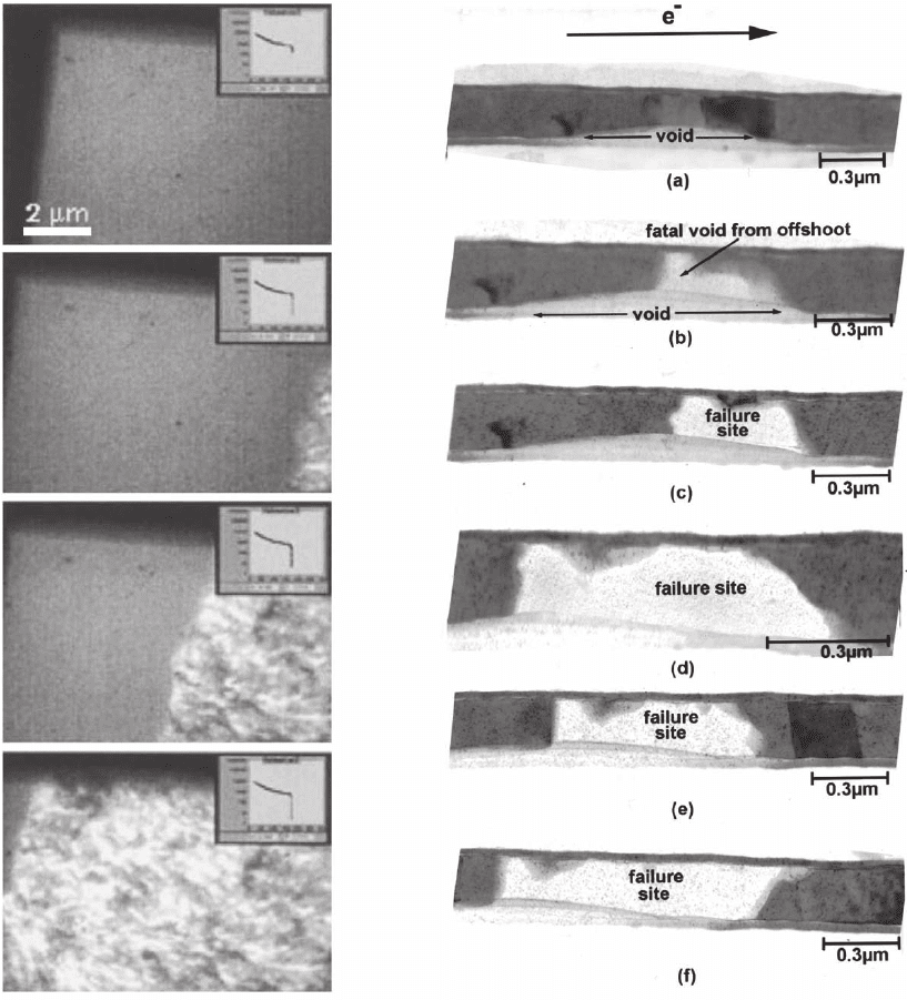
A
B
Figure 6–32. Correlation of resistivity with structure. (A) Video images taken at 15 s time intervals
simultaneously displaying the crystallization of an Al–Ge fi lm at 450K and the accompanying drop
in electrical resistance (insets). The crystallization front can be seen to proceed from the right- to the
left-hand side. (Reprinted with permission from Verheijen et al., © 2004. American Institute of Physics.)
(B) Evolution of a 300 nm wide Al (0.5 wt% Cu) interconnect line, 400 nm thick and 150 mm long on a
20 nm TiN underlayer. Lines are deposited on a SiN/SiO
2
bilayer membrane to minimise changes in
the stress state on heating. 100 nm oxide passivation is added, and the lines are then annealed to form
the bamboo structure (i.e., all grain boundaries run perpendicularly across the line). In situ stressing
is carried out at 320ºC and a current density of 2 × 10
6
Acm
−2
, for (a) 3.5, (b) 4.0, (c) 4.1, (d) 4.5, (e) 4.6
and (f) 5.5 hours. (Reprinted with permission from Lau et al., © 1998 by the American Physical
Society.)
Chapter 6 In Situ Transmission Electron Microscopy 503
and current densities above 10
6
Acm
-2
are used for accelerated testing,
so in some experiments, on-chip heat sink structures are integrated
into the samples (Prybyla et al., 1998).
These studies show that electromigration-induced voids nucleate
well before complete failure of the lines (Riege et al., 1996), and void
dynamics depend on the local grain boundary structure. The failure
mechanism depends on temperature, since at high temperature voids
unpin from grain boundaries while at lower temperatures they grow
at their nucleation site (Prybyla et al., 1998). Interestingly, when TiN
barrier layers are present, voids do not migrate, presumably due to
changes in surface diffusion (Lau et al., 2000). Even thin oxide fi lms
alter electromigration kinetics. Surface diffusion is in fact the domi-
nant failure mechanism if grain boundary motion is hindered (Vook,
1994; Chang and Vook, 1995).
Since a thick passivation layer may be essential for meaningful
results, in some studies the sample is mounted vertically and imaged
in cross section at high voltage (Okabayashi et al., 1996; H. Mori et al.,
1997). Such experiments show mass transport through Al and TiN
layers, as well as vertical void and whisker growth. The measurement
of local strain by CBED during electromigration (Nucci et al., 2005) is
an exciting recent development that promises to relate these in situ
results more closely to models.
6.2 Electrical Measurements on Individual Nanostructures
The experiments described above, where electrical biasing is applied
to a relatively large volume of the specimen, probe several important
phenomena. At the nanoscale, equally interesting information is pro-
vided by biasing individual nanostructures using STM technology.
Commercial TEM/STM holders are in fact becoming increasingly
common for both electrical and mechanical applications (www.
nanofactory.com, www.gatan.com).
As with the mechanical experiments in Sections 5.3.2 and 5.3.3,
carbon nanotubes and Au wires are favored for electrical studies. We
fi rstly discuss CNTs. One can bias a tip on which a tube has been
placed or grown, or equivalently bias the tip and approach a tube on
the substrate. This allows observation of the electric fi eld distribution
at the tip of a biased tube (Cumings et al., 2002), and structural changes
during fi eld emission (Wang et al., 2002b; Kuzumaki et al., 2004; Jin et
al., 2005). The work function of CNTs can be measured and related to
structure (Gao et al., 2001; Bai et al., 2003b; Xu et al., 2005a, b) and CNT
growth can be observed in the gap between a biased tip and the sub-
strate (Yamashita et al., 1999).
If an individual tube is contacted, its conductivity can of course be
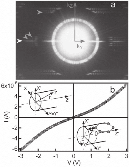
measured. Kociak et al. (2002) were even able to correlate the chiral
indices of double walled tubes, measured using diffraction, with their
transport properties (Figure 6–33). Conductivity measurements show
that CNTs are ballistic conductors at room temperature (Poncharal
et al., 2002), and that the telescoping multiwalled CNTs mentioned in
Section 5.3.3 behave as near-ideal rheostats (Cumings and Zettl, 2004).
504 F.M. Ross
Figure 6–33. Simultaneous structure analy-
sis and measurement of transport properties
for a double-walled nanotube (DWNT). (A)
Experimental diffraction pattern of a DWNT.
The iris-like ring is an artifact. Note the
layered line structure of the diffraction
pattern. The white arrow indicates the equa-
torial line, and the gray ones indicate some
other intensity lines. (B) Current-voltage
characteristic of the same tube. Ohmic behav-
ior is visible up to 0.5 V. Insets: Diffraction
geometry. The upper inset shows the elec-
tron beam oriented along X with (X′, Y′, Z′)
the frame of reference of the MWNT. The
diffraction pattern is recorded in the YZ
plane. In the lower inset, a carbon atom (gray
dot) is characterized by a translation distance
Z
f
o
and a rotation angle Φ
f
o
with respect to
the tube axis. (Reprinted with permission
from Kociak et al., © 2002 by the American
Physical Society.)
Structural changes taking place during current transport have also
been observed (Huang et al., 2005).
The other common material for electrical studies is Au. When thin
wires are formed by touching Au tips to a substrate and then pulling
away, the conductance can be measured and correlated with the struc-
ture. Figure 6–34 demonstrates quantized conductance through single
and double Au chains (Ohnishi et al., 1998b). Single chains in fact show
a metal-insulator transition (Kizuka et al., 2001a). Conductance and
structure change together, showing the dynamic nature of the system
(Kizuka et al., 2001b; Oshima et al., 2003c). Catalytically grown nanow-
ires (Section 3.6) provide another interesting subject for study. Although
Larsson et al. (2004) measured the conductivity of GaAs nanowires,
nanowire electrical properties have generally not been examined in as
much detail as Au wires or CNTs.
For any nanostructure studied in situ, the nature of the contact, for
example how the STM tip is cleaned, is important in ensuring that the
measurements relate to the structure rather than the contact. A drop
of Hg can be used (Poncharal et al., 1999; Wang et al., 2001; Kociak et
al., 2002) to measure properties like work function and quantum con-
ductance, but there are still real issues in creating ohmic contacts to
nanostructures (Larsson et al., 2004) which must be solved before
extending these experiments to a wider range of materials systems.