Hawkes P.W., Spence J.C.H. (Eds.) Science of Microscopy. V.1 and 2
Подождите немного. Документ загружается.

1172 R.E. Dunin-Borkowski et al.
However, the contrast of these fringes decreases as their spacing is
reduced, and the recording process is also dominated by Poisson-
distributed shot noise (Lichte et al., 1987). These parameters are affected
by the illumination diameter, exposure time, and biprism voltage. The
fi nal “phase resolution” (Harscher and Lichte, 1996) and “spatial reso-
lution” are always inherently linked, in the sense that a small phase
shift can be measured with high precision and poor spatial resolution,
or with low precision but high spatial resolution. In each of the exam-
ples described above, the recorded phase images were always smoothed
slightly to remove noise, and the spatial resolution of the magnetic
information was estimated typically to be between 10 and 20 nm. This
procedure is necessarily subjective, and great care is required to ensure
that artifacts are not introduced. Higher spatial and phase resolution
might possibly also be achieved by recording several holograms of
each area of interest and subsequently averaging the resulting phase
images.
4 Measurement of Electrostatic Fields
In this section, the application of electron holography to the character-
ization of electrostatic fi elds is reviewed. Initial examples are taken
from the characterization of electrostatic fringing fi elds outside electri-
cally biased nanowires. The challenges that are associated with imaging
dopant contrast at depletion layers in semiconductors are then
described, before discussing the characterization of interfaces at which
both charge redistribution and changes in chemistry are possible.
4.1 Field-Emitting Carbon Nanotubes
Early experiments on tungsten microtips demonstrated that electron
holography could be used to measure electrostatic fringing fi elds in
biased samples (Matteucci et al., 1992). Further studies were made on
pairs of parallel 1-µm-diameter Pt wires held at different potentials
(Matteucci et al., 1988) and on single conducting wires (Kawasaki
et al., 1993), and simulations were presented for electrostatic phase
plates (Matsumoto and Tonomura, 1996). A more recent example
involves the use of electron holography to map the electrostatic poten-
tial around the end of an electrically biased multiwalled carbon nano-
tube (Cumings et al., 2002). Nanotubes were mounted on a three-axis
manipulation electrode using conducting epoxy and positioned approx-
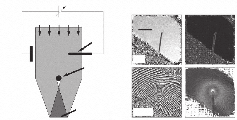
imately 6 µm from a gold electrode, as shown in Figure 18–18a. Depend-
ing on the applied bias, electrons were emitted from the nanotube. The
left hand column of Figure 18–18b shows contoured phase images
recorded before a bias V
b
was applied to the specimen, and for a bias
above the threshold for fi eld emission (approximately 70 V). The upper
phase shift map (V
b
= 0) is featureless around the nanotube, whereas
the lower map (V
b
= 120 V) shows closely spaced 2π phase contours. The
right hand column in Figure 18–18b shows the corresponding phase
gradient for each image. When V
b
= 0, the phase gradient is featureless
around the nanotube, whereas it is concentrated around the nanotube
Chapter 18 Electron Holography 1173
tip when V
b
= 120 V. The images shown in Figure 18–18b were inter-
preted by comparison with simulations, calculated on the assumption
that the nanotube could be approximated by a line charge, where the
charge distribution was varied until a close fi t to the data was found.
The fi t to the 120 V phase data in Figure 18–18b provided a value of
1.22 V/nm for the electric fi eld at the nanotube tip. This fi eld was stable
over time, even when the emission current varied.
4.2 Dopant Potentials in Semiconductors
One of the most elusive yet tantalizing challenges for electron holog-
raphy has been the quest for a reliable, quantitative approach to the
characterization of electrostatic potentials associated with charge
redistribution at depletion regions in doped semiconductors. Attempts
to tackle this problem have been made since the 1960s using many
forms of electron interferometry, both experimentally (e.g., Titchmarsh
et al., 1969; Frabboni et al., 1987) and theoretically (e.g., Pozzi and Vanzi,
1982; Beleggia et al., 2000). It is now recognized that TEM specimen
preparation can have a profound effect on the contrast visible in holo-
graphic phase images of doped semiconductors, either because of
physical damage to the specimen surface or because of the implanta-
tion of dopant ions such as Ar or Ga during ion milling. An electrically
inactive surface layer and/or a doped layer, with a thickness depend-
ing on the specimen preparation method, may form at the sample
surface. In addition, the specimen may charge up during observation,
to such an extent that all dopant contrast is lost. The effects of specimen
V
b
Electron Beam
Nanotube
Biprism
Image Plane
Phase Phase Gradient
ba
200 nm
0 V
120 V
Figure 18–18. (a) Schematic diagram of the experimental set-up used to record electron holograms of
fi eld-emitting carbon nanotubes. (b) Phase shift and phase gradient maps determined from electron
holograms of a single multiwalled carbon nanotube at bias voltages of 0 and 120 V. The phase gradient
indicates where the electric fi eld is strongest. Note the concentration of the electric fi eld at the nanotube
tip when the bias voltage is 120 V. (Reprinted from Cumings et al., 2002.)
1174 R.E. Dunin-Borkowski et al.
preparation, and in particular the electrical state of near-surface regions,
most likely account for many of the anomalous results in early experi-
ments. Recent studies indicate that it may be possible to resolve these
problems.
The fi rst unequivocal demonstration of two-dimensional mapping
of the electrostatic potential in an unbiased doped semicon -
ductor using electron holography was achieved for metal–oxide–
semiconductor (MOS) Si transistors (Rau et al., 1999). The source and
drain regions were visible in phase images with a spatial resolution of
10 nm and an energy resolution of close to 0.10 eV. Differential thinning
was discounted as a cause of the observed phase shifts, and an optimal
specimen thickness of 200–400 nm was identifi ed for such experiments.
The transistors were prepared for TEM examination using conven-
tional mechanical polishing and Ar ion milling. A 25-nm-thick electri-
cally altered layer was identifi ed on each surface of the specimen,
which resulted in measured built-in voltages of 0.9 ± 0.1 V across each
p–n junction, which was lower than the value of 1.0 V predicted for the
specifi ed dopant concentration.
More recently, electron holography studies of transistors have been
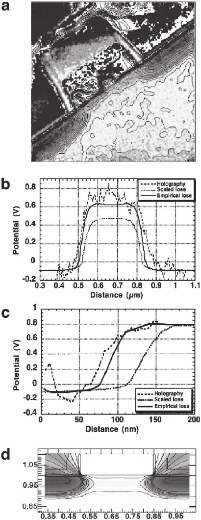
compared with process simulations (Gribelyuk et al., 2002). Figure
18–19a shows a contoured image of the electrostatic potential associ-
ated with a 0.35-µm Si device inferred from an electron hologram,
where the contours correspond to potential steps of 0.1 V. The B-doped
source and drain regions are delineated clearly. In this study, the speci-
men was prepared primarily using tripod wedge-polishing, followed
by limited low-angle Ar ion milling at 3.5 kV. Signifi cantly, no electri-
cally dead surface layer had to be taken into account to quantify the
results. Figure 18–19b and c shows a comparison between line profi les
obtained from Figure 18–19a and simulations, both laterally across the
junction and with depth from the Si surface. Simulations for “scaled
loss” and “empirical loss” models, which account for B-implant segre-
gation into the adjacent oxide and nitride layers, are shown. The scaled
loss model, which leads to stronger B diffusion, assumes uniform B
loss across the device structure, whereas the empirical loss model
assumes segregation of the implanted B at the surfaces of the source
and drain regions. In both Figure 18–19b and Figure 18–19c, the empiri-
cal loss model provides a closer match to the experimental results.
Figure 18–19d shows a simulated electrostatic potential map for the
same device based on the “empirical loss” model, which matches
closely with the experimental image in Figure 18–19a. Overall, this
study demonstrated successful mapping of the electrostatic potential
in 0.13-µm and 0.35-µm device structures with a spatial resolution of
6 nm and a sensitivity of 0.17 eV.
In early applications of electron holography to dopant delineation,
which were carried out on chemically thinned Si samples under condi-
tions of reverse bias (e.g., Frabboni et al., 1985), differences between
phase images recorded at different bias voltages were used to visualize
external electrostatic fringing fi elds close to the positions of p–n junc-
tions. Electrostatic potential profi les have recently been measured
for reverse-biased Si p–n junctions that were prepared for TEM
Chapter 18 Electron Holography 1175
Figure 18–19. (a) Reconstructed maps of the electrostatic potential distribu-
tion in a 0.35-µm semiconductor device structure, with a contour step of 0.1 V,
recorded at an accelerating voltage of 200 kV using a Philips CM200 FEGTEM.
(b) Lateral and (c) depth profi les obtained from the image shown in (a). Predic-
tions from process simulations for “scaled loss” and “empirical loss” models
are also shown. (d) Two-dimensional simulated map of the potential based on
the “empirical loss” model, with a contour step of 0.1 V. The dimensions are
in micrometers. (Reprinted from Gribelyuk et al., 2002.)
1176 R.E. Dunin-Borkowski et al.
examination using focused ion beam milling (Twitchett et al., 2002,
2004, 2005). It is signifi cant to note here that focused ion beam milling
is currently the technique of choice for preparing TEM specimens from
site-specifi c regions of integrated circuits. It is therefore important to
establish whether holography results obtained from unbiased speci-
mens prepared by focused ion beam milling are reliable. It is also
useful to develop a specimen geometry that allows electrical currents
to be passed through TEM specimens prepared using this technique.
Specimens for in situ electrical biasing were prepared by using a 30-
kV FEI 200 focused ion beam workstation to machine parallel-sided
electron-transparent membranes at the corners of 1 × 1-mm 90° cleaved
squares of wafer, as shown schematically in Figure 18–20a. This geom-
etry allowed electrical contacts to be made to the front and back sur-
faces of each specimen using a modifi ed single-tilt holder, as shown in
Figure 18–20b. Care was taken to expose the region of interest to the
focused beam of Ga ions only at a glancing angle to its surface. Figure
18–20c shows a representative holographic phase image recorded from
an unbiased Si p–n junction sample prepared by focused ion beam
milling. The crystalline thickness was measured independently to be
550 nm using convergent beam electron diffraction. The p-type and n-
type regions are delineated clearly as areas of darker and lighter con-
trast, respectively. The additional “gray” band at the specimen edge is
likely to be associated with the presence of an electrically altered layer,
which is visible in cross section but is thought to extend around the
entire specimen surface. No electrostatic fringing fi eld is visible outside
the specimen, indicating that its surface must be an equipotential. Line
profi les across the junction were obtained from phase images acquired
with different reverse bias voltages applied to a specimen of 390 nm
crystalline thickness (Figure 18–20d), as well as from several unbiased
specimens. Each profi le in Figure 18–20d is qualitatively consistent
with the expected potential profi le for a p–n junction in a specimen of
uniform thickness. The height of the potential step across the junction,
∆φ, increases linearly with reverse bias voltage V
appl
, as shown in Figure
18–20e. This behavior is described by the equation
∆φ = C
E
(V
bi
+ V
appl
)t
active
(25)
where C
E
is defi ned in Eq. (7) and the p–n junction is contained in an
electrically active layer of thickness t
active
in a specimen of total thick-
ness t. Measurement of the gradient of Figure 18–20e, which is equal
to C
E
t
active
, provides a value for t
active
of 340 ± 10 nm, indicating that 25
± 5 nm of the crystalline thickness on each surface of the TEM speci-
men is electrically inactive. The intercept with the vertical axis is
C
E
V
bi
t
active
, which provides the expected value for the built-in voltage
across the junction of 0.9 ± 0.1 V. Depletion widths across the junction
measured from the line profi les are higher than expected, suggesting
that the electrically active dopant concentration in the specimen is
lower than the nominal value. These experiments also show that elec-
trical biasing reactivates some of the dopant that has been passivated
by specimen preparation (Dunin-Borkowski et al., 2002). Figure 18–20f
shows a four-times-amplifi ed phase image obtained from a 90° cleaved
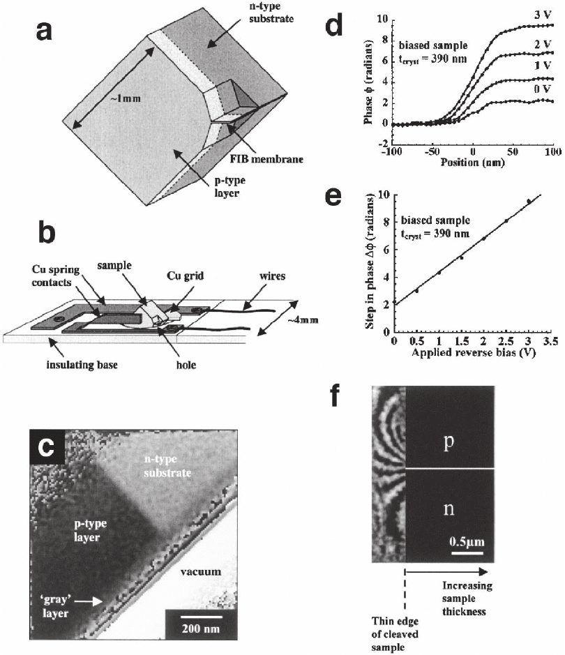
Figure 18–20. (a) Schematic diagram showing the specimen geometry used for applying external
voltages to focused ion beam milled semiconductor device specimens containing p–n junctions in situ
in the TEM. In the diagram, focused ion beam (FIB) milling has been used to machine a membrane
of uniform thickness that contains a p–n junction at one corner of a 90° cleaved wedge. (b) Schematic
diagram showing the specimen position in a single tilt electrical biasing holder. The specimen is glued
to the edge of a Cu grid using conducting epoxy and then clamped between two spring contacts on
an insulating base. (c) Reconstructed phase image acquired from an unbiased Si sample containing a
p–n junction. Note the “gray” layer running along the edge of the specimen, which is discussed in the
text. No attempt has been made to remove the 2π phase “wraps” at the edge of the specimen. (d) Phase
shift measured across a p–n junction as a function of reverse bias for a single sample of 390 nm crystal-
line thickness (measured using convergent beam electron diffraction). (e) The height of the measured
step in phase across the junction is shown as a function of reverse bias. (f) Four times-amplifi ed
reconstructed phase image, showing the vacuum region outside a p–n junction in a 2-V reverse-biased
cleaved wedge sample that had not been focused ion beam milled. (Reprinted from Twitchett et al.,
2002.)
1178 R.E. Dunin-Borkowski et al.
wedge that had not been prepared by focused ion beam milling, for an
applied reverse bias of 2 V, where an external electrostatic fringing fi eld
is visible. Such fringing fi elds were never observed outside unbiased
cleaved wedges or any focused ion beam milled specimens, indicating
that the surfaces of the present TEM specimens prepared by focused
ion beam milling are equipotentials under applied bias.
The importance of minimizing and assessing damage, implantation,
and specimen thickness variations when examining focused ion beam
milled TEM specimens that contain p–n junctions has been highlighted
by results from unbiased samples (Wang et al., 2002a–c, 2005). The
most elegant of these experiments involved the use of focused ion
beam milling to form a 45° specimen thickness profi le, from which
both the phase change across the junction and the absolute phase shift
relative to vacuum on each side of the junction could be plotted as a
function of specimen thickness. The slopes of the phase profi les were
then used to determine the built-in voltage across the junction, the
mean inner potentials on the p and n sides of the junction, and the
electrically altered layer thickness. Using this approach, the built-in
voltage across a junction with a dopant concentration of approximately
10
15
cm
−3
was measured to be 0.71 ± 0.05 V, while the mean inner poten-
tials of the p and n sides of the junction were measured to be 11.50 ±
0.27 and 12.1 ± 0.40 V, respectively. The electrically altered layer thick-
ness was measured to be approximately 25 nm on each surface of the
specimen.
The electrical nature of the surface of a TEM specimen that contains
a doped semiconductor can be assessed by comparing experimental
holography results with simulations. Such a comparison, performed
using commercial semiconductor process simulation software
(Beleggia et al., 2001), suggests that electron beam-induced positive
charging of the surface of a TEM specimen, at a level of 10
13
–10
14
cm
−2
,
creates an inversion layer on the p-side of the junction. This layer may
explain the absence of electrostatic fringing fi elds outside the specimen
surface, which would otherwise dominate the observed phase contrast
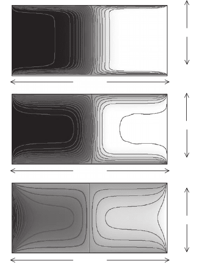
(Dunin-Borkowski and Saxton, 1996). Figure 18–21 shows the results
of an alternative set of numerical simulations, in which semiclassical
equations are used to determine the charge density and potential in a
parallel-sided Si sample that contains a p–n junction. The Fermi level
on the surface of the specimen is set to a single value to ensure that it
is an equipotential (Somodi et al., 2005). The simulations in Figure 18–
21 are for symmetrical junctions with dopant concentrations of 10
18
,
10
17
, and 10
16
cm
−3
. Contours of spacing 0.05 V are shown in each fi gure.
As either the dopant concentration or the specimen thickness decreases,
a correspondingly smaller fraction of the specimen retains electrical
properties that are close to those of the bulk device. In the simulations,
the average step in potential across the junction through the thickness
of the specimen, which is insensitive to the surface state energy, is
reduced from that in the bulk device. This reduction is greatest for low
sample thicknesses and low dopant concentrations. In practice, as a
result of additional complications from oxidation, physical damage,
and implantation, the simulations shown in Figure 18–21 are likely to
Chapter 18 Electron Holography 1179
be an underestimate of the full modifi cation of the potential from that
in the original device.
The ways in which the sample preparation technique of “wedge-
polishing” affects both the dead layer thickness and specimen charg-
ing have been explored experimentally for a one-dimensional p–n
junction in Si by McCartney et al. (2002). A specimen was prepared
from a p-type wafer that had been subjected to a shallow B implant
and a deeper P implant, resulting in the formation of an n-type well
and a p-doped surface region. Phase images were obtained before and
after coating one side of the specimen with approximately 40 nm of
carbon. Profi les obtained from the uncoated sample showed an initial
increase in the measured phase going from vacuum into the specimen,
then dropping steeply and becoming negative at large thicknesses.
This behavior was not observed after carbon coating, suggesting that
it is associated with sample charging that results from the electron
beam-induced emission of secondary electrons.
Similar charging effects can be seen directly in two dimensions in
Figure 18–22. Figure 18–22a shows a bright-fi eld image of a linear array
300 nm
300 nm
300 nm
a
b
c
n
p
n
p
n
p
150 nm
700 nm
1500 nm
Figure 18–21. Simulations of electrostatic potential distributions in parallel-
sided slabs of thickness 300 nm containing abrupt, symmetrical Si p–n junc-
tions formed from (a) 10
18
, (b)10
17
, and (c) 10
16
cm
−3
of Sb (n-type) and B (p-type)
dopants. The potential at the specimen surfaces is 0.7 eV above the Fermi level,
and contours of spacing 0.05 V are shown. The horizontal scale is different in
each fi gure to show the variation in potential close to the position of the junc-
tion. The simulations were generated using a two-dimensional rectangular
grid. (Reprinted from Somodi et al., 2005.)
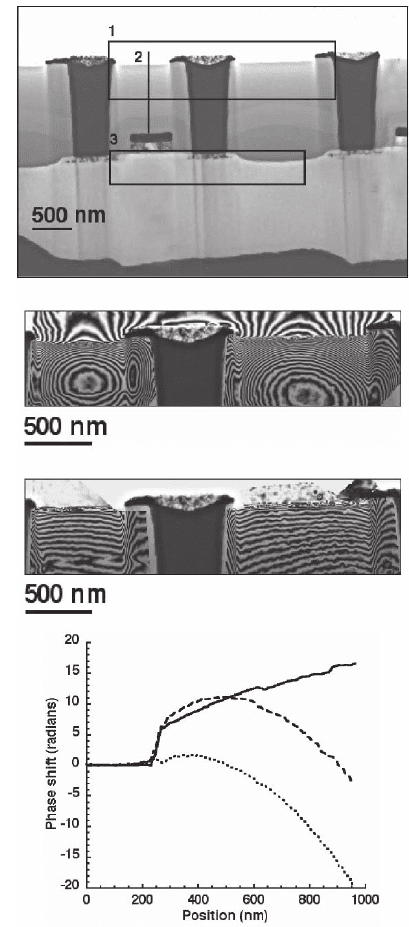
1180 R.E. Dunin-Borkowski et al.
b
c
d
a
Figure 18–22. Results obtained from a cross-
sectional semiconductor device specimen of
nominal thickness 400 nm prepared using con-
ventional “trench” focused ion beam milling. (a)
Bright-fi eld TEM image of a PMOS (0.5-µm gate)
transistor, which forms part of a linear array of
similar transistors, indicating the locations of
the regions analyzed in more detail in the sub-
sequent fi gures. The dark bands of contrast
above the transistors are W contacts. Thickness
corrugations are visible in the Si substrate in
each image. The gates are formed from W sili-
cide, while the amorphous layers above the
gates and between the W plugs are formed from
Si oxides that have different densities. (b) Eight
times-amplifi ed phase contours were calculated
by combining phase images from several holo-
grams obtained across the region marked “1” in
(a) using a microscope accelerating voltage of
200 kV and a biprism voltage of 160 V. Specimen
charging results in the presence of electrostatic
fringing fi elds in the vacuum region outside the
specimen edge, as well as elliptical phase con-
tours within the Si oxide layers between the W
contacts. (c) An equivalent phase image obtained
after coating the specimen on one side with
approximately 20 nm of carbon to remove the
effects of charging. The phase contours now
follow the expected mean inner potential con-
tribution to the phase shift in the oxide layers,
and there is no electrostatic fringing fi eld outside
the specimen edge. (d) One-dimensional line
profi les obtained from the phase images in (b)
and (c) along the line marked “2” in (a). The
dashed and solid lines were obtained before
and after coating the specimen with carbon,
respectively. The dotted line shows the differ-
ence between the solid and dashed lines.
(Reprinted from Dunin-Borkowski et al., 2005.)
of transistors, which were originally located ∼5 µm below the surface
of a wafer and separated from its surface by metallization layers. Such
transistors present a signifi cant but representative challenge for TEM
specimen preparation for electron holography both because the metal-
lization layers are substantial and can result in thickness corrugations
in the doped regions of interest and because these overlayers must, at
least in part, be removed to provide a vacuum reference wave for elec-
tron holography. An additional diffi culty results from the possibility
that the overlayers, which contain silicon oxides, may charge during
Chapter 18 Electron Holography 1181
examination in the electron microscope. Conventional “trench” focused
ion beam milling (Park, 1990; Szot et al., 1992) was used to prepare the
specimen, which has a nominal thickness of 400 nm. Figure 18–22b
shows eight-times-amplifi ed phase contours obtained from the region
marked “1” in Figure 18–22a. Instead of the expected phase distribu-
tion, which should be proportional to the mean inner potential multi-
plied by the specimen thickness, elliptical contours are visible in each
oxide region, and an electrostatic fringing fi eld is present outside the
specimen (at the top of Figure 18–22b). Both the elliptical contours and
the fringing fi eld are associated with the build-up of positive charge
in the oxide layer. The elliptical contours are centered is several hun-
dreds of nanometers from the specimen edge. Figure 18–22c shows a
similar phase image obtained after coating the specimen on one side
with approximately 20 nm of carbon. The effects of charging are now
absent, there is no fringing fi eld outside the specimen edge, and the
phase contours follow the change in specimen thickness. One-dimen-
sional phase profi les were generated from the phase images used to
form Figure 18–22b and c along the line marked “2” in Figure 18–22a,
and are shown in Figure 18–22d. The dashed and solid lines corre-
spond to results obtained before and after coating the specimen with
carbon, respectively, while the dotted line shows the difference between
the solid and dashed lines. If the charge is assumed to be distributed
through the thickness of the specimen, then the electric fi eld in the
oxide is approximately 2 × 10
7
V/m. Th i s value is just below the break-
down electric fi eld for thermal SiO
2
of 10
8
V/m (Sze, 2002). Equivalent
results obtained from a specimen of 150 nm nominal thickness show
that the elliptical contours are closer to the specimen edge. The effect
of specimen charging on the dopant potential (in the source and drain
regions of the transistors) is just as signifi cant. The phase gradient
continues into the substrate, and the dopant potential is undetectable
before carbon coating, whether or not a phase ramp is subtracted from
the images. If focused ion beam milling from the substrate side of the
wafer (Schwarz et al., 2003) is used, then specimen charging no longer
occurs, presumably as a result of Si redeposition onto the specimen
surface. McCartney et al. (2003) provide an overview of this and other
techniques for the preparation of semiconductor devices for electron
holography.
Although questions still remain about phase contrast observed at
simple p–n junctions, electron holographic data have been interpreted
from more complicated semiconductor device structures, in which
changes in composition as well as doping concentration are present.
One example is a strained n-Al
0.1
Ga
0.9
N/In
0.1
Ga
0.9
N/p-Al
0.1
Ga
0.9
N hetero-
junction diode, in which strong piezoelectric and polarization fi elds
are used to induce high two-dimensional electron gas concentrations
(McCartney et al., 2000). To interpret experimental measurements of
the potential profi le across the heterojunction, after corrections for
specimen thickness changes (assuming a linear thickness profi le and
neglecting contributions to the measured phase from variations in
mean inner potential), additional charge had to be added to simula-
tions. In particular, a sheet of negative charge was included at the
