Hawkes P.W., Spence J.C.H. (Eds.) Science of Microscopy. V.1 and 2
Подождите немного. Документ загружается.

1162 R.E. Dunin-Borkowski et al.
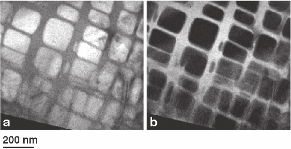
of closely spaced crystals. Figure 18–12 shows chemical maps of a
crystalline region of a naturally occurring magnetite–ulvöspinel
(Fe
3
O
4
–Fe
2
TiO
4
) mineral specimen, which has exsolved during slow
cooling to yield an intergrowth of magnetite-rich blocks separated by
nonmagnetic ulvöspinel-rich lamellae (Price, 1981). The Fe and Ti
chemical maps shown in Figure 18–12 were obtained using three-
window background-subtracted elemental mapping with a Gatan
imaging fi lter. Exsolution lamellae subdivide the grain into a fairly
regular array of magnetite-rich blocks. The specimen thickness
increases from 70 nm at the top of the region to 195 nm at the bottom.
The magnetite blocks are, therefore, roughly equidimensional. Rema-
nent magnetic states were recorded by tilting the specimen in zero fi eld
and then turning the objective lens on fully to saturate the sample, to
provide a known starting point from which further fi elds could be
applied. The objective lens was then turned off, the specimen tilted in
zero fi eld in the opposite direction, and the objective lens was excited
partially to apply a known in-plane fi eld component to the specimen
in the opposite direction. The objective lens was switched off and the
sample tilted back to 0° in zero fi eld to record each hologram. This
a
d
b
c
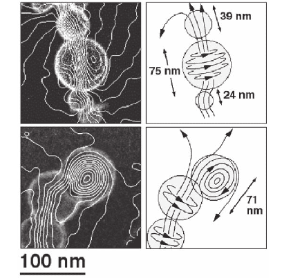
Figure 18–11. (a and b) Experimental phase contours showing the strength of
the local magnetic induction (integrated in the electron beam direction) in two
different chains of Fe
0.56
Ni
0.44
particles, recorded with the electron microscope
objective lens switched off. The particle diameters are (a) 75 nm between two
smaller particles and (b) 71 nm at the end of a chain. Contours, whose spacings
are 0.083 and 0.2 radians for images (a) and (b), respectively, have been over-
laid onto oxygen maps of the particles recorded using a Gatan imaging fi lter.
The mean inner potential contribution to the measured phase shift has been
removed from each image. (c and d) Schematic representations of the magnetic
microstructure in the chains. Magnetic vortices spinning about the chain axis
are visible in (c) and (d). A vortex spinning perpendicular to the chain axis is
also visible in (d). (Reprinted from Dunin-Borkowski et al., 2004b.)
Chapter 18 Electron Holography 1163
procedure was repeated for a number of different applied fi elds
(Harrison et al., 2002). Mean inner potential contributions to the
measured phase shifts were removed using a procedure different from
that used for the chains and rings of nanoparticles described above.
Although both thickness and composition vary in the magnetite–
ulvöspinel specimen, the different compositions of magnetite and
ulvöspinel are compensated by their densities in such a way that their
mean inner potentials are exactly equal. As a result, only a thickness
correction is required. The local specimen thickness across the region
of interest was determined in units of inelastic mean free path by using
energy-fi ltered imaging. This thickness measurement was then used
to determine the mean inner potential contribution to the phase shift,
which was in turn used to establish the magnetic contribution to the
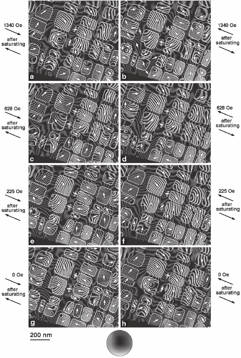
phase. Figure 18–13 shows eight of the resulting remanent magnetic
states recorded after applying the in-plane fi elds indicated. The black
contour lines provide the direction and magnitude of the magnetic
induction in the plane of the sample, which can be correlated with the
positions of the magnetite blocks (outlined in white). The direction of
the induction is also indicated using colors and arrows, according to
the color wheel shown at the bottom of the fi gure. Figure 18–13 shows
that the magnetic domain structure in this sample is extremely complex.
In Figure 18–13, the smallest block observed to form a vortex is larger
than the predicted minimum size of 70 nm for vortices to form in
isolated cubes of magnetite. The abundance of single domain states
implies that they have lower energy than vortex states in the presence
of strong interactions. The demagnetizing energy, which normally
destabilizes the single domain state with respect to the vortex state in
isolated particles, is greatly reduced in an array of strongly interacting
particles.
Figure 18–12. Three-window background-subtracted elemental maps
acquired from a naturally occurring titanomagnetite sample with a Gatan
imaging fi lter using (a) the Fe L edge and (b) the Ti L edge. Brighter contrast
indicates a higher concentration of Fe and Ti in (a) and (b), respectively.
(Reprinted from Dunin-Borkowski et al., 2004b.)
1164 R.E. Dunin-Borkowski et al.

Chapter 18 Electron Holography 1165
3.3.5 Lithographically Patterned Magnetic Nanostructures
Specimen preparation presents a challenge for many samples of inter-
est that contain nanostructured magnetic materials. One example is
provided by nanomagnet arrays that have been fabricated directly onto
an Si substrate using interferometric lithography (Ross, 2001). Figure
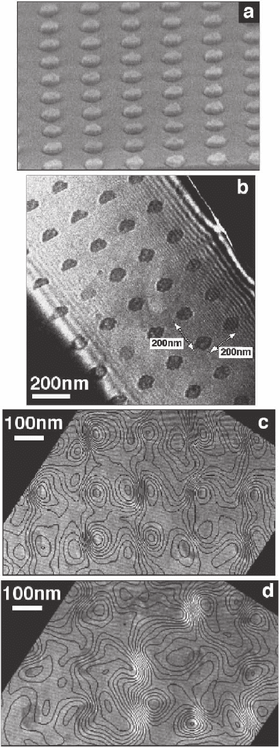
18–14a shows a scanning electron microscope image of nominally 100-
nm-diameter 20-nm-thick Co dots fabricated on Si in a square array of
side 200 nm. The dots were prepared for TEM examination using
focused ion beam milling in plan-view geometry, by micromachining
a trench from the substrate side of the specimen to leave a free-
standing 10 × 12-µm membrane of crystalline Si, which was approxi-
mately 100 nm in thickness and contained over 3000 Co dots. Figure
18–14b shows an off-axis electron hologram recorded from part of the
electron-transparent membrane containing the dots. The specimen was
tilted slightly away from zone axis orientations of the underlying Si
substrate to minimize diffraction contrast. The specimen edge is toward
the bottom left of the fi gure (Dunin-Borkowski et al., 2001). Figure 18–
14c and d shows contours of spacing 0.033 ≈ π/94 radians that have
been added to the (slightly smoothed) magnetic contribution to the
holographic phase, for two different remanent magnetic states of the
Co dots. In Figure 18–14c, which was recorded after saturating the dots
upward and then removing the external fi eld, the dots are oriented
magnetically in the direction of the applied fi eld. In contrast, in Figure
18–14d, which was formed by saturating the dots upward, applying a
382 Oe downward fi eld and then removing the external fi eld, the dots
are magnetized in a range of directions. The experiments show that
the dots are sometimes magnetized out of the plane (e.g., at the bottom
left of Figure 18–14d). The measured saturation magnetizations are
smaller than expected for pure Co, possibly because of oxidation or
damage sustained during specimen preparation. Similar electrode-
posited 57-nm-diameter 200-nm-high Ni pillars arranged in square
arrays of side 100 nm, which were prepared for TEM examination using
focused ion beam milling in a cross-sectional geometry, have also been
examined. Despite their shape, not all of the Ni pillars were magne-
tized parallel to their long axes. Instead, they interacted with each
other strongly, with two, three, or more adjacent pillars combining to
form vortices.
Figure 18–13. Magnetic phase contours from the region shown in Figure 8–12,
measured using electron holography. Each image was acquired with the speci-
men in magnetic fi eld-free conditions. The outlines of the magnetite-rich
regions are marked in white, while the direction of the measured magnetic
induction is indicated both using arrows and according to the color wheel
shown at the bottom of the fi gure (red = right, yellow = down, green = left,
blue = up). Images (a), (c), (e), and (g) were obtained after applying a large
(>10,000 Oe) fi eld toward the top left, then the indicated fi eld toward the
bottom right, after which the external magnetic fi eld was removed for holo-
gram acquisition. Images (b), (d), (f), and (h) were obtained after applying
identical fi elds in the opposite directions. (Reprinted from Harrison et al.,
2002.) (See color plate.)
䉳
1166 R.E. Dunin-Borkowski et al.
Figure 18–14. (a) Scan-
ning electron micro-
scope image of 100-nm-
diameter 20-nm-thick
Co dots fabricated on
Si in a square array of
side 200 nm using inter-
ferometric lithography.
(b) Off-axis electron
hologram of part of an
electron-transparent
membrane containing
the dots, prepared using
focused ion beam
milling. The hologram
was acquired at 200 kV
using a Philips CM200
FEGTEM, a biprism
voltage of 160 V, a holo-
graphic interference
fringe spacing of 3.05 nm,
and an overlap width of
1.04 µm. (c and d) Mag-
netic con tributions to
the measured electron
holographic phase shift
for two remanent mag-
netic states. The contour
spacing is 0.033 radians:
(c) was formed by satu-
rating the dots upward
and then removing the
external fi eld; (d) was
formed by saturating
the dots upward, apply-
ing a 382 Oe downward
fi eld, and then removing
the external fi eld.
(Reprinted from Dunin-
Borkowski et al., 2001.)
Chapter 18 Electron Holography 1167
Results similar to those shown in Figure 18–14 have been obtained
from a wide range of larger lithographically patterned structures,
many of which show multidomain behavior (Dunin-Borkowski et al.,
2000; Hu et al., 2005; Heumann et al., 2005). Few phase contours are
visible outside such elements when they support magnetic fl ux closure
states. Electron holography has also been used to provide information
about magnetic interactions between closely separated ferromagnetic
layers within individual Co/Au/Ni spin-valve elements (Smith et al.,
2000). The presence of two different contour spacings at different
applied fi elds in such elements is associated with the reversal of the
magnetization direction of the Ni layer in each element before the
external fi eld is reduced to zero as a result of fl ux closure associated
with the strong fringing fi eld of the magnetically more massive and
closely adjacent Co layer.
3.3.6 Co Nanowires
An important question relates to the minimum size of a nanostructure
in which magnetic fi elds can be characterized successfully using elec-
tron holography. This point is now addressed through the character-
ization of 4-nm-diameter single crystalline Co nanowires (Snoeck
et al., 2003). The diffi culty of this measurement results from the fact
that the mean inner potential contribution to the phase shift at the
center of a 4-nm wire relative to that in vacuum is 0.57 radians (assum-
ing a value for V
0
of 22 V), whereas the step in the magnetic contribu-
tion to the phase shift across the wire is only 0.032 radians (assuming
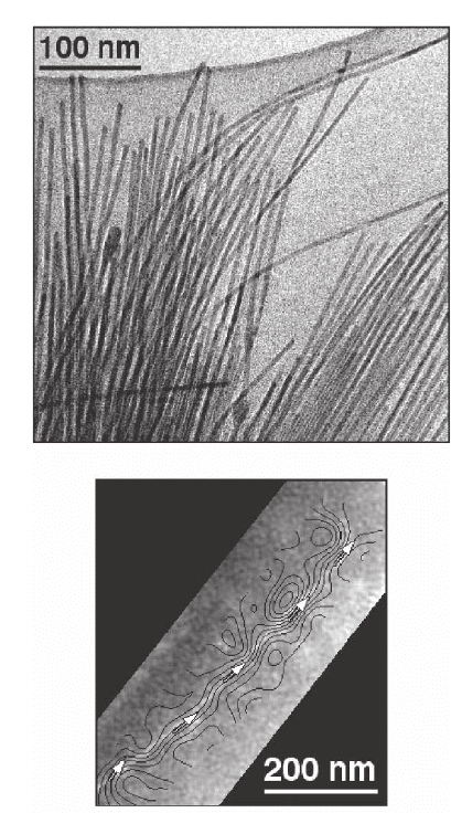
a value for B of 1.6 T). Figure 18–15a shows a bright-fi eld TEM image
of a bundle of 4-nm-diameter Co wires, which are each between a few
hundred nanometers and several hundred micrometers in length.
Magnetic contributions to the phase shift were obtained by recording
two holograms from each area of interest, where the wires were mag-
netized parallel and then antiparallel to their length by tilting the
sample by ±30° about an axis perpendicular to the wire axis and using
the conventional microscope objective lens to apply a large in-plane
fi eld to the specimen. The lens was then switched off and the sample
returned to zero tilt to record each electron hologram. This procedure
relies on the ability to reverse the magnetization in the sample exactly,
which is a good assumption for these narrow and highly anisotropic
wires. Figure 18–15b shows the magnetic contribution to the measured
phase shift for an isolated wire, in the form of contours that are spaced
0.005 radians apart. The contours have been overlaid onto an image
showing the mean inner potential contribution to the phase shift, so
that they can be correlated with the position of the wire. The magnetic
signal is weak and noisy, and was smoothed before forming the con-
tours. The closely spaced contours along the length of the wire confi rm
that it is magnetized along its axis. The fact that they are not straight
is intriguing. However, this effect may result from smoothing of the
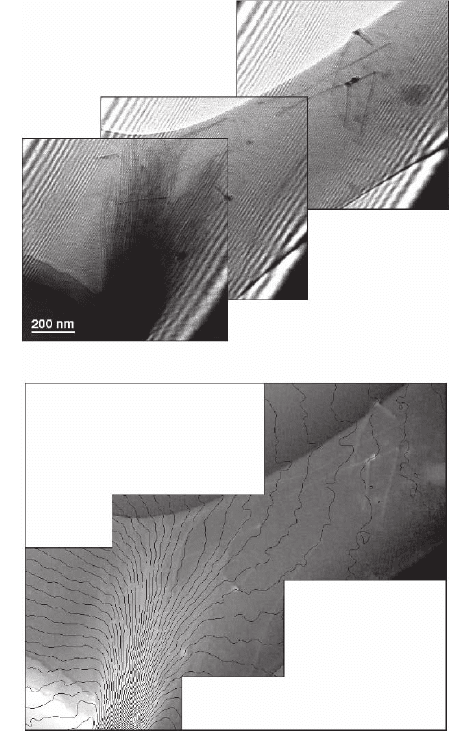
signal, which is noisy and weak. Figure 18–16a shows a montage of
three holograms obtained close to the end of a bundle of Co wires,
which was magnetized approximately parallel to its length. The
magnetic contribution to the measured phase shift is shown in Figure
1168 R.E. Dunin-Borkowski et al.
18–16b in the form of contours, which are spaced 0.25 radians apart.
The wires channel the magnetic fl ux effi ciently along their length, and
they fan out as the fi eld decreases in strength at the end of the bundle.
Although the signal from the bundle appears overall to obscure that
from individual wires and junctions, these details can be recovered by
increasing the density of the contours (Snoeck et al., 2003). The slight
asymmetry between the contours on either side of the bundle in Figure
18–16b may result from the fact that the reference wave is affected by
the magnetic leakage fi eld of the bundle, which acts collectively as
though it were a single wire of larger diameter. The step in phase across
the bundle is (9.0 ± 0.2) radians, which is consistent with the presence
of (280 ± 7) ferromagnetically coupled wires.
a
b
Figure 18–15. (a) Bright-fi eld image of the end of a bundle of Co nanowires
adjacent to a hole in a carbon support fi lm. (b) Contours (0.005 radian spacing)
generated from the magnetic contribution to the phase shift for a single iso-
lated Co nanowire, superimposed onto the mean inner potential contribution
to the measured phase shift. (Reprinted from Snoeck et al., 2003.)
Chapter 18 Electron Holography 1169
3.3.7 Cross-Sectional Specimens
One of the most challenging problems for electron holography of mag-
netic materials is the quantitative measurement of the magnetic prop-
erties of nanometer-scale magnetic layers when examined in cross
section. The primary diffi culty is the presence of rapid and unknown
variations in both the composition and the thickness of the specimen,
from which the weak magnetic signal must be separated. In a cross-
sectional sample, the effects of variations in specimen thickness on the
measurements cannot be eliminated by using the normalized ampli-
tude of the hologram [Eq. (14)], both because the mean free path in
each material in such a cross-sectional specimen is usually unknown
a
b
Figure 18–16. (a) Montage of three electron holograms acquired from the end of a bundle of Co
nanowires. The biprism voltage is 210 V, the acquisition time for each hologram 16 s, the holographic
interference fringe spacing is 3.9 nm, and the holographic overlap width is 1160 nm. No objective aper-
ture was used. (b) Magnetic remanent state, displayed in the form of contours (0.25 radian spacing),
generated from the measured magnetic contribution to the electron holographic phase shift after satu-
rating the wires in the direction of the axis of the bundle. The contours are superimposed onto the
mean inner potential contribution to the phase shift. (Reprinted from Snoeck et al., 2003.)
1170 R.E. Dunin-Borkowski et al.
and because the amplitude image is in general noisy and may contain
strong contributions from diffraction and Fresnel contrast. However,
by rearranging Eqs. (8) and (16), it can be shown that specimen thick-
ness effects may be removed by plotting the difference in the phase
gradient between images in which the magnetization has reversed
divided by the average of their phases, multiplied by a constant and
by the value of the mean inner potential of each magnetic layer sepa-
rately. Formally, this procedure can be written
CVxy
e
dxydx
xy
E
,,
,
0
(
)
(
)
[]
(
)
∆φ
φ
==
(
)
−
(
)
[]
{}
(
)
(
)
⊥
⊥
∫
∆Bxy
eC V x y B xytxydx
,
,,,
E
1
0
ttxy,
(
)
(23)
According to Eq. (23), by combining phase profi les and their gradients
(evaluated in a direction perpendicular to the layers) from successive
holograms with the magnetization direction reversed, the specimen
thickness profi le can be eliminated and the magnetic induction in each
layer determined quantitatively. Both the magnitude and the sign of
∆B
⬜
(x,y) = 2B
⬜
(x,y) are obtained exactly using Eq. (23) if the magnetiza-
tion reverses exactly everywhere in the sample. (The denominator on
the right-hand side of the equation is then unity.) Furthermore, nonzero
values are returned only in regions where the magnetization has
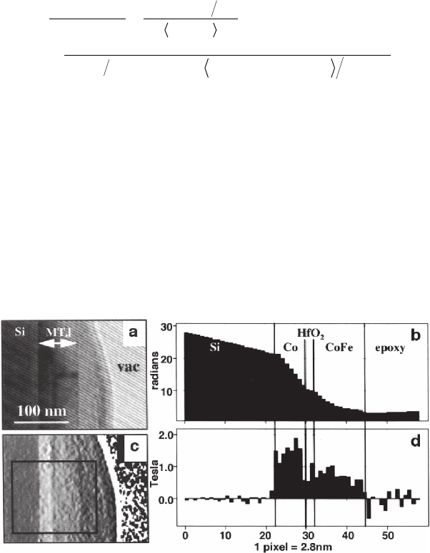
changed. Figure 18–17 illustrates the application of Eq. (23) to a cross-
sectional magnetic tunnel junction that contains a layer sequence of
22 nm Co/4 nm HfO
2
/36 nm CoFe on an Si substrate (McCartney and
Figure 18–17. (a) Off-axis electron hologram obtained from a magnetic tunnel
junction containing a 4-nm HfO
2
tunnel barrier. (b) Measured phase profi le
across the layers in the tunnel junction structure. (c) Image formed by record-
ing two holograms with opposite directions of magnetization in the specimen,
and subsequently taking the difference between the recorded phase gradients
(calculated in a direction perpendicular to the layers) and dividing by the
average of the two phases. (d) Measured magnetic induction in the tunnel
junction sample, generated by multiplying a line profi le obtained from image
(c) by a constant (see text for details), with the vertical scale now plotted in
units of Tesla. (Reprinted from McCartney and Dunin-Borkowski, 1998.)

Chapter 18 Electron Holography 1171
Dunin-Borkowski, 1998). Two holograms were obtained, similar to that
shown in Figure 18–17a, between which the magnetization directions
of the Co and CoFe layers in the specimen were reversed in situ in the
electron microscope. Figure 18–17b shows an unwrapped phase profi le
obtained from the hologram in Figure 18–17a by taking a line profi le
in the direction perpendicular to the layers. Phase profi les from the
two holograms appeared almost identical irrespective of the direction
of magnetization. The application of Eq. (23) to the two phase images
results in the image shown in Figure 18–17c. The line profi le in Figure
18–17d was obtained by averaging Figure 18–17c parallel to the direc-
tion of the layers. As predicted, Figure 18–17d, which should by now
be independent of variations in composition and specimen thickness,
is nonzero only in the magnetic layers and yields a value for the mag-
netic induction in the Co layer of 1.5 T (assuming a mean inner poten-
tial of 25 V). In a similar experiment, holograms of La
0.5
Ca
0.5
MnO
3
have
recently been acquired both above and below the Curie temperature
of the material to remove specimen thickness and mean inner potential
contributions from the measured phase (Loudon et al., 2003).
3.4 Quantitative Measurements, Micromagnetic Simulations,
and Resolution
A particular strength of electron holography is its ability to provide
quantitative information about magnetic properties. For example, the
magnetic moment of a nanoparticle can be obtained from the
relation
m
ey
xydxdy
x
x
x
y
y
=
()
()
=−∞
=+∞
=−∞
=+∞
∫∫
∂
∂
φ
mag
,
(24)
where φ
mag
is the magnetic contribution to the phase shift and y is a
direction perpendicular to x in the plane of the specimen. According
to Eq. (24), the magnetic moment in a given direction can be obtained
by measuring the area under the fi rst differential of φ
mag
evaluated in
the perpendicular direction. The contribution of stray magnetic fi elds
to the moment is included in this calculation if the integration is carried
out over a large enough distance from the particle.
The need to compare electron holographic measurements with
micromagnetic simulations results from the sensitivity of the magnetic
domain structure in nanoscale materials and devices to their detailed
magnetic history. Differences in the starting magnetic states on a scale
that is too small to be distinguished visually, as well as interelement
coupling and the presence of out-of-plane magnetic fi elds, are all
important for the formation of subsequent domain states, and, in par-
ticular, to the sense (the handedness) with which magnetic vortices
unroll (Dunin-Borkowski et al., 1999). The sensitivity of the domain
structure to such effects emphasizes the need to correlate high quality
experimental holographic measurements with micromagnetic
simulations.
The spatial resolution that can be achieved in phase images is deter-
mined primarily by the spacing of the holographic interference fringes.
