Guozhong Cao. Nanostructures & Nanomaterials: Synthesis, Properties & Applications
Подождите немного. Документ загружается.

3
06
Nanostructures and Nanomaterials
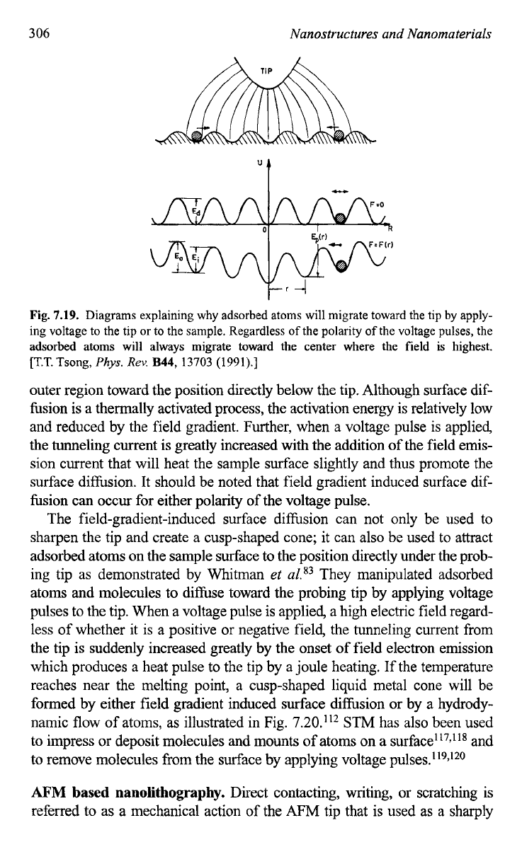
Fig.
7.19.
Diagrams explaining why adsorbed atoms will migrate toward the tip by apply-
ing voltage to the tip
or
to the sample. Regardless
of
the polarity
of
the voltage pulses, the
adsorbed atoms will always migrate toward the center where the field is highest.
[T.T.
Tsong,
Phys.
Rev.
B44,
13703
(1991).]
outer region toward the position directly below the tip. Although surface dif-
hsion is a thermally activated process, the activation energy is relatively low
and reduced by the field gradient. Further, when a voltage pulse is applied,
the tunneling current is greatly increased with the addition of the field emis-
sion current that will heat the sample surface slightly and thus promote the
surface diffusion. It should be noted that field gradient induced surface dif-
hsion can occur for either polarity of the voltage pulse.
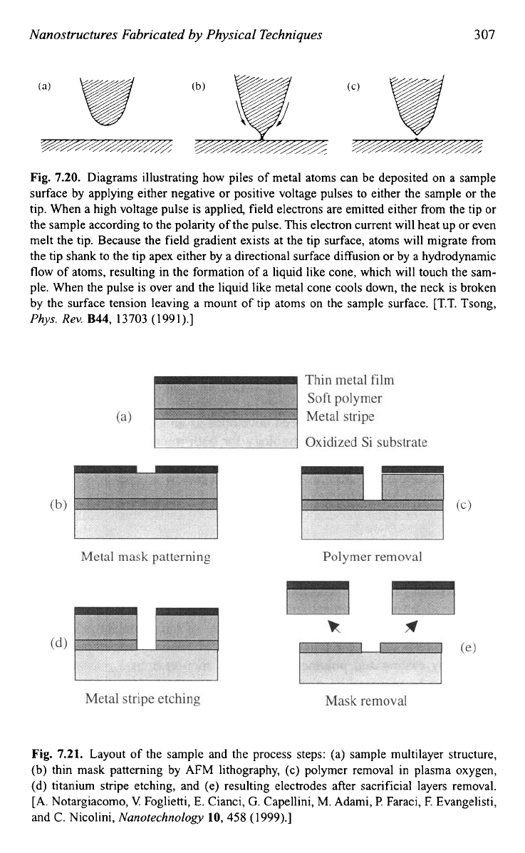
The field-gradient-induced surface diffusion can not only be used to
sharpen the tip and create a cusp-shaped cone; it can also be used to attract
adsorbed atoms on the sample surface to the position directly under the prob-
ing tip as demonstrated by Whitman
et
aLE3
They manipulated adsorbed
atoms and molecules to diffuse toward the probing tip by applying voltage
pulses to the tip. When a voltage pulse is applied, a high electric field regard-
less of whether
it
is a positive or negative field, the tunneling current from
the tip is suddenly increased greatly by the onset of field electron emission
which produces a heat pulse to the tip by a joule heating. If the temperature
reaches near the melting point, a cusp-shaped liquid metal cone will be
formed by either field gradient induced surface diffusion or by a hydrody-
namic
flow
of atoms, as illustrated in Fig.
7.2O.lI2
STM has also been used
to impress or deposit molecules and mounts of atoms on a surface117J18 and
to remove molecules from the surface
by
applying voltage
pulse^."^^'*^
AFM
based
nanolithography.
Direct contacting, writing, or scratching is
referred to as a mechanical action of the
AFM
tip that is used as a sharply
Nanostructures Fabricated by Physical Techniques
3
07
Fig.
7.20.
Diagrams illustrating how piles of metal atoms can be deposited on a sample
surface by applying either negative
or
positive voltage pulses to either the sample
or
the
tip. When a high voltage pulse
is
applied, field electrons are emitted either from the tip
or
the sample according to the polarity of the pulse. This electron current will heat up
or
even
melt the tip. Because the field gradient exists at the tip surface, atoms will migrate from
the tip shank to the tip apex either by a directional surface diffusion
or
by a hydrodynamic
flow of atoms, resulting in the formation of a liquid like cone, which will touch the sam-
ple. When the pulse is over and the liquid like metal cone cools down, the neck is broken
by the surface tension leaving a mount of tip atoms on the sample surface.
[T.T.
Tsong,
Phys.
Rev.
B44,
13703
(1991).]
Fig.
7.21.
Layout of the sample and the process steps: (a) sample multilayer structure,
(b) thin mask patterning by AFM lithography, (c) polymer removal in plasma oxygen,
(d) titanium stripe etching, and (e) resulting electrodes after sacrificial layers removal.
[A. Notargiacomo,
V
Foglietti,
E.
Cianci, G. Capellini, M. Adami,
P.
Faraci, F. Evangelisti,
and
C.
Nicolini,
Nanotechnology
10,
458
(1999).]
308
Nanostructures and Nanomaterials
pointed tool in order to produce fine grooves
on
sample ~urfaces.~~~-'~~
Although direct scratching creates grooves with high precision, low quality
results are often obtained due to tip wear during the process.
An
alternative
approach is to combine scratching on a soft resist polymer layer, such as
PMMA or polycarbonate, as a mask for the etching process and subsequent
etching to transfer the pattern to the sample surface. This method ensures
reduced tip damage, but also precludes
an
accurate alignment to the structures
underneath. A two-layer mask has been investigated as a hrther improvement.
For example, a mask coating consisting
of
a thin layer of polycarbonate of
50-100m
and a film of easy-to-deform and fusible metal such as indium or
tin was used to create
50nm
wide structures.125 Figure
7.21
is the typical
layout of the sample and the process steps with AFM lith~graphy.'~~
7.4.
Soft
Lithography
Soft lithography is a general term describing a set of non-photolithographic
techniques for microfabrication that are based on the printing of
SAMs
and
molding of liquid precursors.
Soft
lithography techniques include contact
printing, micromolding in capillaries, microtransfer molding and replica
molding. Soft lithography has been developed as an alternative to photoli-
thography and a replication technology for both micro- and nanofabrica-
tion. The techniques of soft lithography were developed at Whitesides'
group and have been summarized in excellent review articles.12c128 In this
section, only a brief introduction to the method will be presented.
7.4.1.
Microconfact printing
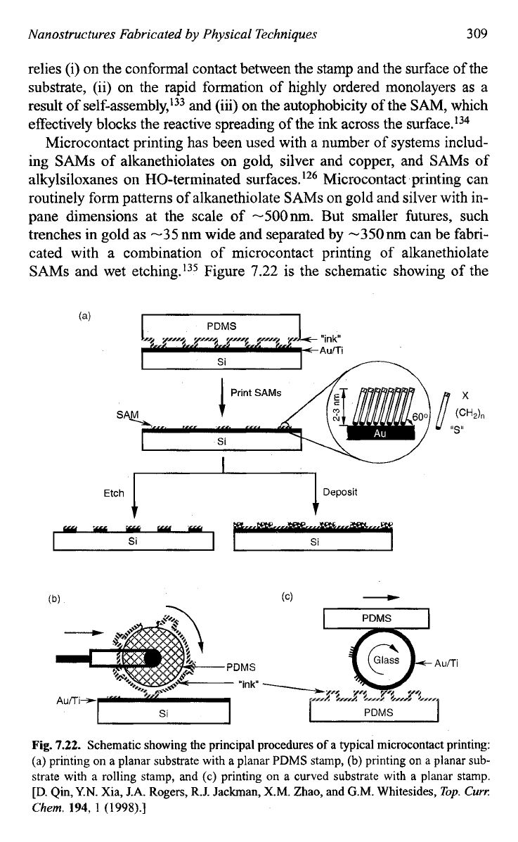
Microcontact printing is a technique that uses an elastomeric stamp with
relief
on
its surface to generate patterned
SAMs
on the surface of both pla-
nar and curved ~ubstrate.'*~~*~~ The procedure
of
microcontact printing is
experimentally simple and inherently parallel. The elastomeric stamp is fab-
ricated by casting and polymerizing
PDMS
monomer in a master mold,
which can be prepared by photolithography or other relevant techniques.
The stamp with a desired pattern is brought in contact with "ink", a solution
to form a SAM on the surface of the stamp. The inked stamp then contacts
a substrate and transfers the
SAM
onto the substrate surface with patterned
structure. A very important advantage that the microcontact printing offers
over other patterning techniques is the capability to fabricate a patterned
structure on a curved ~urface.'~','~* The success
of
microcontact printing
Nanostructures Fabricated by Physical Techniques
309
relies (i) on the conformal contact between the stamp and the surface of the
substrate, (ii) on the rapid formation of highly ordered monolayers as a
result
of
self-a~sembly,'~~ and (iii) on the autophobicity
of
the
SAM,
which
effectively blocks the reactive spreading of the ink across the surface.134
Microcontact printing has been used with a number of systems includ-
ing
SAMs
of alkanethiolates on gold, silver and copper, and SAMs of
alkylsiloxanes on HO-terminated surfaces.
126
Microcontact printing can
routinely form patterns of alkanethiolate SAMs on gold and silver with in-
pane dimensions at the scale
of
-500nm. But smaller futures, such
trenches in gold as -35 nm wide and separated by -350 nm can be fabri-
cated with a combination of microcontact printing of alkanethiolate
SAMs and wet etching.*35 Figure
7.22
is the schematic showing of the
Etch
1
Deposit
I
Fig.
7.22.
Schematic showing the principal procedures
of
a typical microcontact printing:
(a) printing on a planar substrate with a planar PDMS stamp,
(b)
printing on a planar
sub-
strate with a rolling stamp, and
(c)
printing on a curved substrate with
a
planar stamp.
[D. Qin,
Y.N.
Xia, J.A. Rogers, R.J. Jackman, X.M. Zhao, and G.M. Whitesides,
Top.
Cum
Chern.
194,
1
(1998).]
310
Nanostructures and Nanomaterials
principal procedures of a typical microcontact printing: (a) printing on a
planar substrate with a planar
PDMS
stamp,
(b)
printing on a planar sub-
strate with a rolling stamp, and (c) printing on a curved substrate with a
planar stamp.7
7.4.2.
Molding
A
number of molding techniques have been developed for the fabrication
of microstructures, but are also capable of fabricating nanostructures.
These techniques include micromolding in ~apillaries,'~~ microtransfer
molding,'37 and replica m01ding.I~~ An elastomeric
(PDMS)
stamp with
relief on its surface is central to each of these procedures. In micromold-
ing in capillaries, a liquid precursor wicks spontaneously by capillary
action into the network of channels formed by conformal contact between
an elastomeric stamp and a substrate. In microtransfer molding, the
recessed regions of an elastomeric mold are filled with a liquid precursor,
and the filled mold is brought into contact with a substrate. After solidi-
fying, the mold is removed, leaving a micro- or nanostructure on the sub-
strate. Micromolding in capillaries can only be used to fabricate
interconnected structures, whereas microtransfer molding is capable of
generating both isolated and interconnected structures. In replica molding,
micro- or nanostructures are directly formed by casting and solidifying a
liquid precursor against an elastomeric mold. This method is effective for
replicating feature sizes ranging from -30 nm to several centimeters and
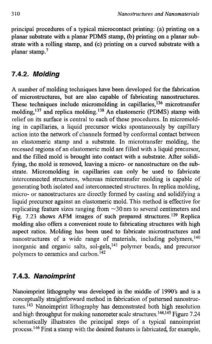
Fig. 7.23 shows AFM images of such prepared structures.139 Replica
molding also offers a convenient route to fabricating structures with high
aspect ratios. Molding has been used to fabricate microstructures and
nanostructures of a wide range of materials, including polymers,'40
inorganic and organic salts, sol-gels,
14'
polymer beads, and precursor
polymers to ceramics and carbon.14*
7.4.3.
Nanoimprint
Nanoimprint lithography was developed in the middle of
1990's
and is a
conceptually straightforward method in fabrication of patterned nanostruc-
tures.
143
Nanoimprint lithography has demonstrated both high resolution
and high throughput for making nanometer scale structures.
144y145
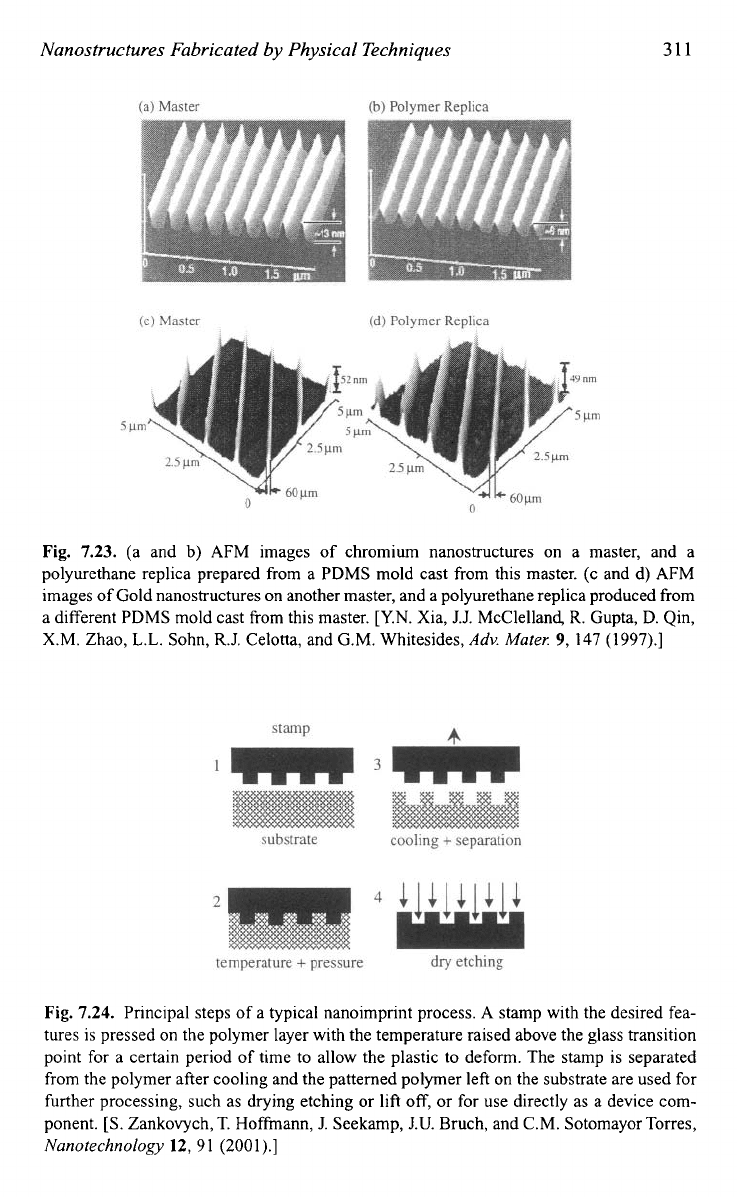
Figure 7.24
schematically illustrates the principal steps of a typical nanoimprint
process.146 First a stamp with the desired features is fabricated, for example,
Nanostructures Fabricated by Physical Techniques
311
Fig.
7.23.
(a and
b)
AFM images of chromium nanostructures on a master, and a
polyurethane replica prepared from a PDMS mold cast from this master. (c and d) AFM
images of Gold nanostructures on another master, and a polyurethane replica produced from
a different PDMS mold cast from this master.
[Y.N.
Xia,
J.J.
McClelland
R.
Gupta, D. Qin,
X.M.
Zhao,
L.L.
Sohn,
R.J.
Celotta, and G.M. Whitesides,
Adv.
Muter
9,
147 (1997).]
Fig.
7.24.
Principal steps of a typical nanoimprint process.
A
stamp with the desired fea-
tures
is
pressed on the polymer layer with the temperature raised above the glass transition
point for a certain period of time to allow the plastic to deform. The stamp
is
separated
from the polymer after cooling and the patterned polymer left on the substrate are used for
further processing, such as drying etching
or
lift off,
or
for use directly as a device com-
ponent.
[S.
Zankovych, T. Hoffinann,
J.
Seekamp,
J.U.
Bruch, and C.M. Sotomayor Torres,
Nanotechnology 12,
91 (2001).]
3
12 Nanostructures and Nanomaterials
by optical or electron beam lithography followed by
dry
etching or reactive
ion etching. The material to be printed, typically a thermoplastic polymer, is
spun onto a substrate where the nanostructures are to be fabricated, The sec-
ond step is to press the stamp on the polymer layer with the temperature
raised above the glass transition point for a certain period of time to allow
the plastic to deform. In the third step, the stamp is separated from the poly-
mer after cooling. The patterned polymer left on the substrate is used for
fur-
ther processing, such as dry etching or lift-off, or for use directly as a device
component. Although the process is technically straightforward, there are
several key issues that require special attention to make the process com-
petitive as a nanofabrication technology as briefly summarized below.
146
The first challenge for the nanoimprint lithography is the multilevel
capability or the ability of exact alignment of multilayers. Various
approaches have been explored to achieve exact alignment including use
of commercially available stepper and aligner.'47-149 Stamp size should be
controlled, since large stamp size may introduce potential drawback, such
as the parallelity of the substrate and stamp and thermal gradients in print-
ing.I5O The
flow
of the displaced polymer could set a limit to the feature
density that imprinting stamps can achieve. Imprint of
50
nm features sep-
arated by
50
nm spaces within an area
of
200
X
200
Fm2 has been demon-
~trated.'~~ Sticking is another challenge to the nanoimprint lithography.
Ideally, there should be no sticking at all between the polymer layers to be
imprinted and the stamp. The choice of printing temperature, the visco-
elastic properties of the polymer and the interfacial energy are among the
key fa~t0rs.I~~
Processing control includes printing temperature and pressure and cur-
ing time. In principle, both temperature and pressure should be chosen as
low as possible in view of the time needed for temperature and pressure
cycling. Pressure is less important, since its application takes only a
minute or
so;
more significant may be the rate at which pressure is
increased, again with respect to the mechanical recovery of the polymer.
Various nanostructured devices have been demonstrated by nanoimprint
lithography. For example, InP/GaInAs two-dimensional electron gas
three-terminal ballistic junction devices were fabricated using NIL.
152
Si02/Si stamps fabricated by electron beam lithography and reactive ion
etching were used to transfer sub-
100
nm features into a high-mobility
InP-based two-dimensional electron gas material. After NIL, the resist
residues are removed in oxygen plasma and followed by wet etching
of InP/GaInAs to create the desired three-terminal junctions devices.
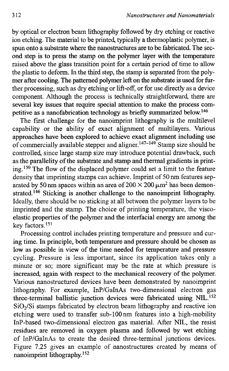
Figure
7.25
gives an example of nanostructures created by means of
nanoimprint lithography.
152
Nanostructures Fabricated by Physical Techniques
313
Fig.
7.25.
SEM image
of
a device structure in InP/GaInAs with electron waveguide
(A) and three-terminal ballistic junction (B) areas fabricated by nanoimprint lithography.
Electrode (1) is a side gate used to control electron waveguide (2); gate
(3)
controls the
TBJ
(4)
device. The voltages on the TBJ electrodes are denoted
V,, V,,
and
V,.
[I.
Maximov,
I?
Carlberg,
D.
Wallin, I. Shorubalko,
W.
Seifert, H.Q.
Xu, L.
Montelius, and
L.
Samuelson,
Nanotechnology
13,
666
(2002).]
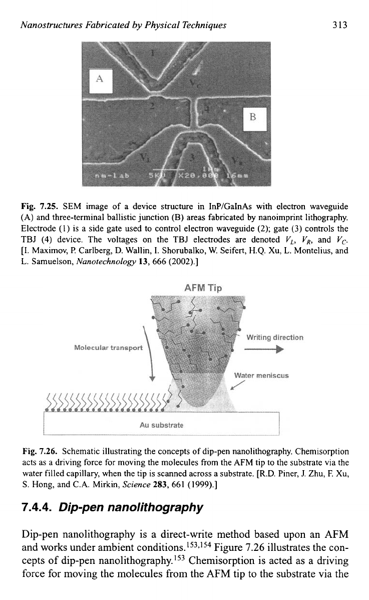
Fig.
7.26.
Schematic illustrating the concepts of dip-pen nanolithography. Chemisorption
acts as a driving force
for
moving the molecules from the AFM tip to the substrate via the
water filled capillary, when the tip is scanned across a substrate.
[R.D.
Piner, J. Zhu,
F.
Xu,
S.
Hong, and C.A. Mirkin,
Science
283,
661
(1999).]
7.4.4.
Dip-pen nanolithography
Dip-pen nanolithography is a direct-write method based upon an AFM
and works under ambient
condition^.'^^,'^^
Figure
7.26
illustrates the con-
cepts of dip-pen nan01ithography.I~~ Chemisorption is acted as a driving
force for moving the molecules from the AFM tip to the substrate via the
3
14
Nanostructures and Nanomaterials
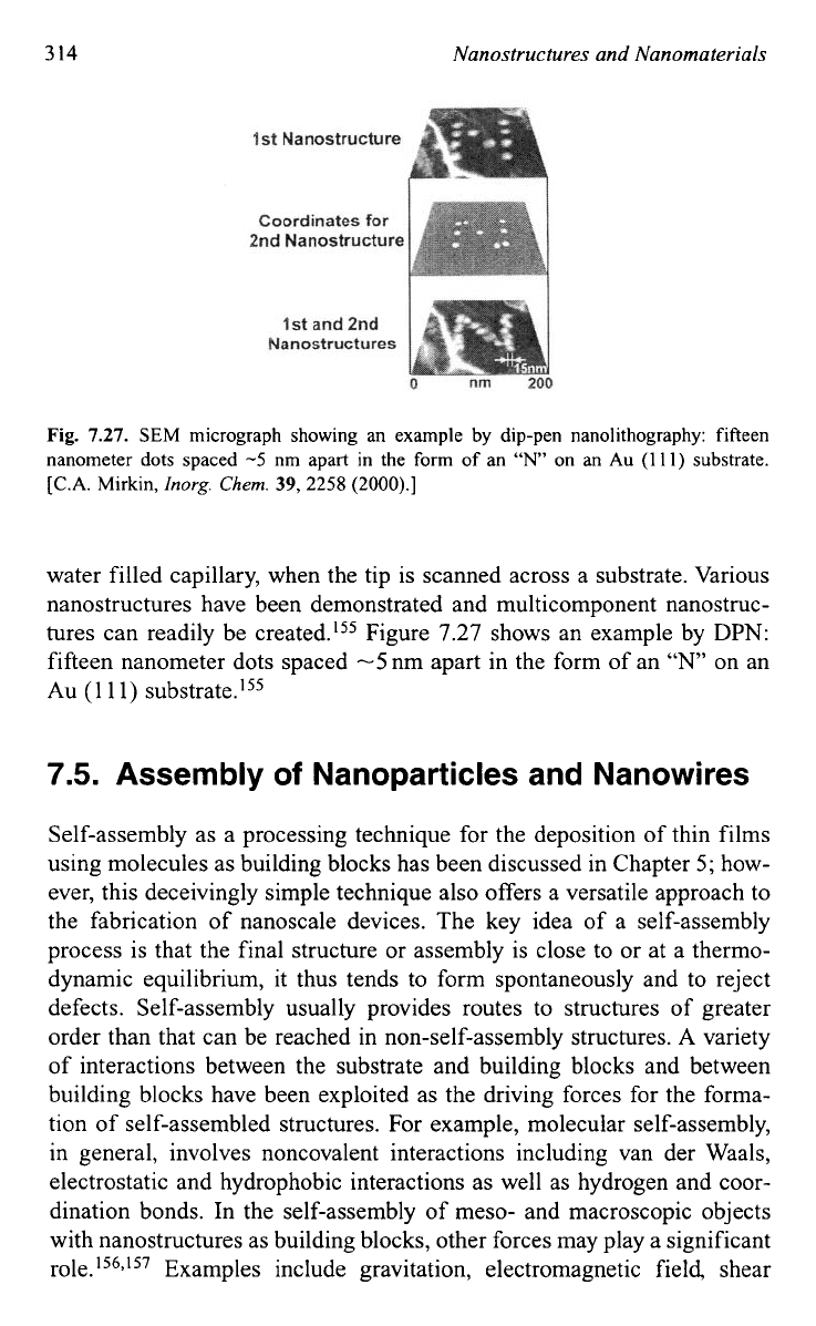
Fig.
7.27.
SEM
micrograph showing an example by dip-pen nanolithography: fifteen
nanometer dots spaced
-5
nm apart in the
form
of an
“N’
on an
Au
(1
11)
substrate.
[C.A.
Mirkin,
Znorg.
Chern.
39,2258
(2000).]
water filled capillary, when the tip
is
scanned across a substrate. Various
nanostructures have been demonstrated and multicomponent nanostruc-
tures can readily be created.’55 Figure
7.27
shows an example by
DPN:
fifteen nanometer dots spaced
-5
nm apart in the form of an
“N”
on an
Au
(1
11)
~ubstrate.’~~
7.5.
Assembly
of
Nanoparticles and Nanowires
Self-assembly as a processing technique for the deposition of thin films
using molecules as building blocks has been discussed in Chapter
5;
how-
ever, this deceivingly simple technique also offers a versatile approach to
the fabrication of nanoscale devices. The key idea of a self-assembly
process is that the final structure or assembly is close to or at a thermo-
dynamic equilibrium, it thus tends to form spontaneously and to reject
defects. Self-assembly usually provides routes to structures of greater
order than that can be reached in non-self-assembly structures.
A
variety
of interactions between the substrate and building blocks and between
building blocks have been exploited as the driving forces for the forma-
tion of self-assembled structures. For example, molecular self-assembly,
in general, involves noncovalent interactions including van der Waals,
electrostatic and hydrophobic interactions as well as hydrogen and coor-
dination bonds. In the self-assembly of meso- and macroscopic objects
with nanostructures as building blocks, other forces may play a significant
ro1e.’56,’57 Examples include gravitation, electromagnetic field, shear
Nanostructures Fabricated
by
Physical Techniques
315
force, capillary and entropy.
158
Although the fabrication of functional
nanoscale devices is still a subject
of
intensive research and many new
techniques are being discovered, the following discussion will provide a
general picture about the most commonly used approaches in the self-
assembly of nanoclusters and nan~crystal'~~-'~' and nanorods.16*
7.5.1.
Capillary
forces
One of the commonly used strategies of self-assembly of nanoparticles into
ordered
2D
arrays is based on the lateral capillary interactions. The origin
of the lateral capillary forces is the deformation of the liquid surface, which
is supposed to be flat in the absence
of
particles. The magnitude of the cap-
illary interaction between two colloidal particles is directly proportional to
the interfacial deformation created by the particles. The capillary interac-
tions between two adjacent particles either floating on the liquid-air
surface or partially immersed into a liquid film on a substrate are briefly
introduced below.
163
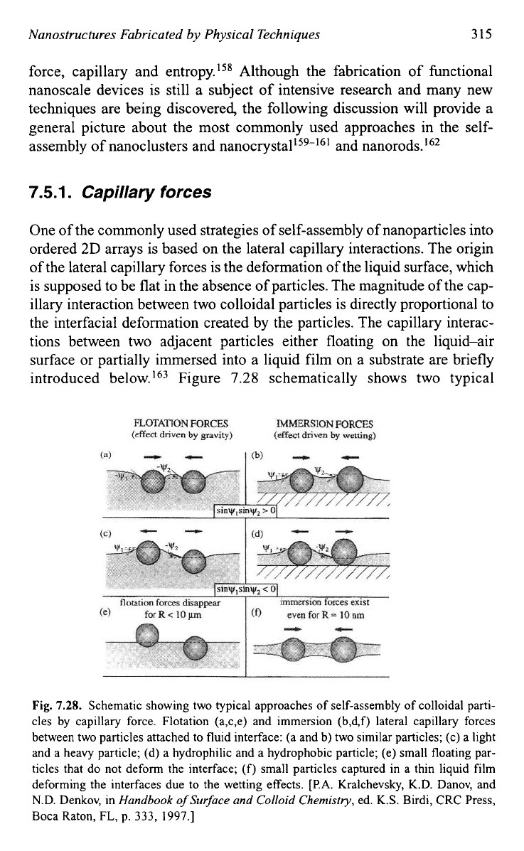
Figure
7.28
schematically shows two typical
Fig.
7.28. Schematic showing two typical approaches of self-assembly of colloidal parti-
cles by capillary force. Flotation (a,c,e) and immersion (b,d,f) lateral capillary forces
between two particles attached to fluid interface: (a and b) two similar particles; (c) a light
and a heavy particle; (d) a hydrophilic and a hydrophobic particle; (e) small floating par-
ticles that do not deform the interface; (f) small particles captured in a thin liquid film
deforming the interfaces due to the wetting effects. [P.A. Kralchevsky, K.D. Danov, and
N.D. Denkov, in
Handbook
of
Surface and
Colloid
Chemistry,
ed.
K.S.
Birdi, CRC Press,
Boca Raton, FL, p.
333,
1997.1