Guozhong Cao. Nanostructures & Nanomaterials: Synthesis, Properties & Applications
Подождите немного. Документ загружается.

286
Nanostructures and Nanomaterials
(ii) electron column (beam forming system), (iii) mechanical stage and
(iv) control computer which is used to control the various machine sub-
systems and transfer pattern data to the beam deflection systems.
Electron sources applicable to electron beam lithography are the same
as those used in conventional electron microscopes. These sources can be
divided into two groups: thermionic and field emission. Thermionic guns
rely on the emission of electrons from a material that
is
heated above a
critical temperature beyond which electrons are emitted from the surface.
These sources are prepared from materials such as tungsten, thoriated
tungsten, or lanthanum hexaboride. Field emission sources use a high
electric field surrounding a very sharp point of tungsten. The electric field
extracts electrons at the tip of the source, forming a Gaussian spot of only
a few tens of angstroms in diameter.
It
is impossible to deflect an electron beam to cover a large area, in a
typical electron beam lithography system, mechanical stages are required
to move the substrate through the deflection field of the electron beam
column. Stages can be operated in a stepping mode in which the stage is
stopped, an area of the pattern written and then the stage moved to a new
location where an adjacent pattern area is exposed. Alternatively, stages
can be operated in a continuous mode where the pattern is written on the
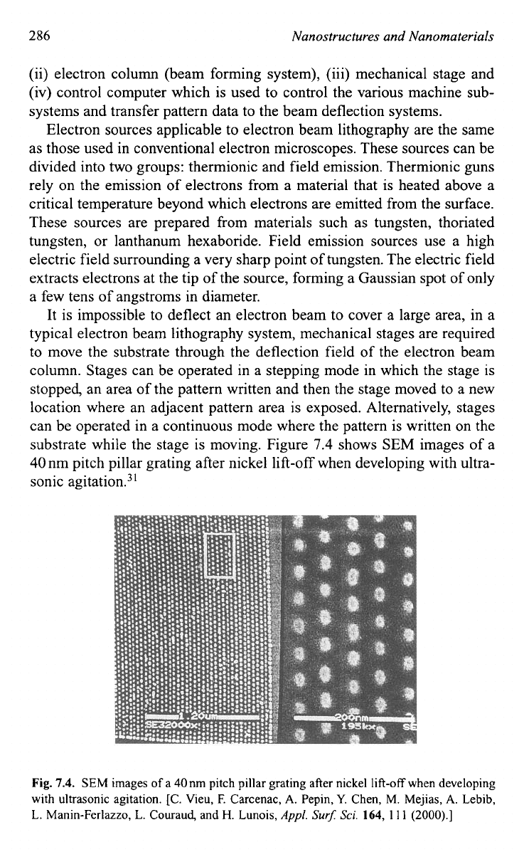
substrate while the stage is moving. Figure
7.4
shows SEM images of a
40
nm pitch pillar grating after nickel lift-off when developing with ultra-
sonic agitati~n.~'
Fig.
7.4.
SEM images
of
a
40
nm pitch pillar grating after nickel lift-off when developing
with ultrasonic agitation. [C. Vieu,
F.
Carcenac,
A.
Pepin,
Y.
Chen, M. Mejias,
A.
Lebib,
L. Manin-Ferlazzo, L. Couraud, and
H.
Lunois,
Appl.
Surf
Sci.
164,
11
1
(2000).]
Nanostructures Fabricated by Physical Techniques
287
7.2.4.
X-ray lithography
X-rays with wavelengths in the range of
0.04
to
0.5
nm represent another
alternative radiation source with potential for high-resolution pattern
replication into polymeric resist materials.33 X-ray lithography was first
demonstrated that to obtain high-resolution patterns using X-ray proxim-
ity printing by Spears and Smith.34 The essential ingredients in X-ray
lithography include:
(1)
A mask consisting of a pattern made with an X-ray absorbing mate-
(2)
An X-ray source of sufficient brightness in the wavelength range of
(3)
An X-ray sensitive resist material.
There are two X-ray radiation sources: (i) electron impact and (ii) syn-
chrotron sources. Conventional electron impact sources produce a broad
spectrum of X-rays, centered about a characteristic line
of
the material,
which are generated by bombardment of a suitable target material by
a
high energy electron beam. The synchrotron or storage ring produces
a broad spectrum of radiation stemming from energy loss of electrons
in motion at relativistic energies. This radiation is characterized by an
intense, continuous spectral distribution from the infrared to the long
wavelength X-ray region. It is highly collimated and confined near the
orbital plane of the circulating electrons, thereby requiring spreading in
the vertical direction of moving the mask and wafer combination with
constant speed through the fan of synchrotron radiation. Synchrotrons
offer the advantage of high power output.
Absorption of an X-ray photon results in the formation of a photoelec-
tron which undergoes elastic and inelastic collisions within the absorbing
material producing secondary electrons which are responsible for the
chemical reactions in the resist film. The range of the primary photoelec-
trons is on the order of
100-200
nm.
A
major limitation is that of penum-
bral shadowing, since the X-ray source is finite in size and separated from
the mask and the edge of the mask does not cast a sharp shadow.
Low
mask contrast is another factor that degrades the pattern resolution. It is
very important to keep the radiation source in a small area in order to min-
imize penumbral shadowing and with a maximum intensity of X-rays
to minimize exposure time. X-ray proximity lithography is known
to
pro-
vide a one to one replica of the features patterned on the mask, and the
resolution limit of the X-ray lithography is
-25
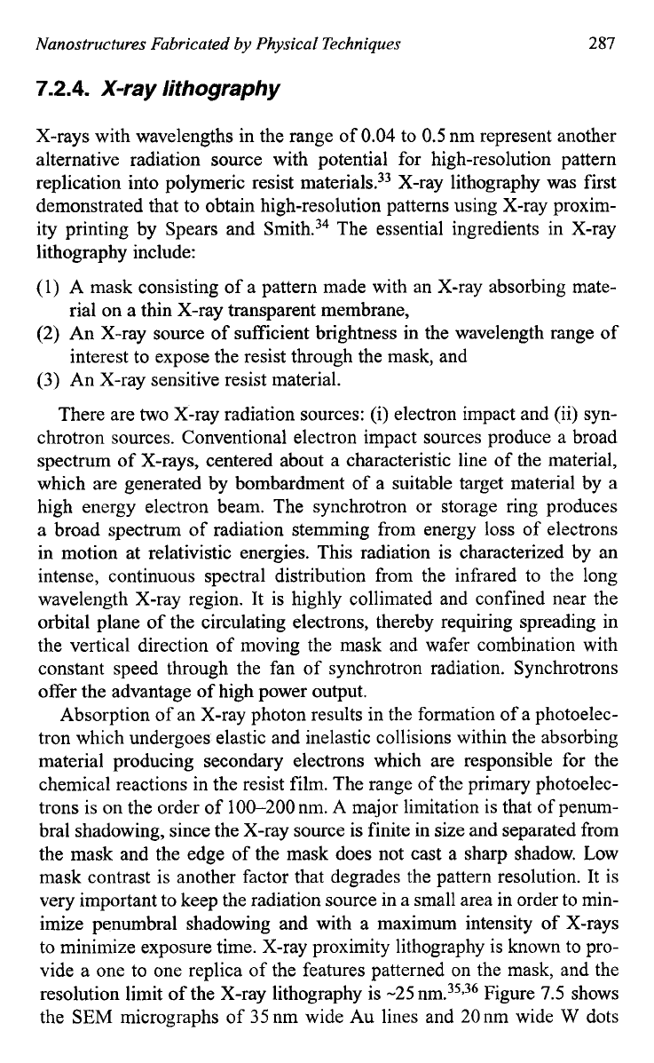
nm.35,36 Figure
7.5
shows
the
SEM
micrographs
of 35
nm wide Au lines and
20
nm wide
W
dots
rial on a thin X-ray transparent membrane,
interest to expose the resist through the mask, and
288
Nanostructures and Nanomaterials
Fig.
7.5.
(a) 35 nm wide
Au
lines grown by electroplating using a template fabricated by
X-ray lithography. The mean thickness is about
450
nm, which corresponds to an aspect
ratio close to 13. (b) 20 nm wide
W
dots obtained after reactive ion etching of 1250nm
thick
W
layer. [G. Simon,
A.M.
Haghiri-Gosnet,
J.
Bourneix, D. Decanini,
Y.
Chen,
F.
Rousseaux, H. Launios, and B. Vidal,
.I
Vac.
Sci.
Techno/.
B15,
2489 (1997).]
fabricated by electroplating and reactive ion etching in combination with
X-ray lith~graphy.~~
7.2.5.
Focused ion beam (FIB) lithography
Since the development of liquid metal ion (LMI) source in
1975,37
focused ion beam has been rapidly developed into a very attractive tool in
lithography, etching, deposition, and doping3* Since scattering of ions in
the MeV range is several orders of magnitude less than that for electrons,
ion beam lithography has long been recognized to offer improved resolu-
tion.39,40 The commonly used FIBS are Ga and Au-Si-Be alloys LMI
sources due to their long lifetime and high ~tability.~',~* FIB lithography
is capable of producing electronic devices with submicrometer dimen-
sion~.~~ The advantages of FIB lithography include its high resist exposure
sensitivity, which is
two
or more orders of magnitude higher than that of
Nanostructures Fabricated by Physical Techniques
289
electron beam lithography, and its negligible ion scattering in the resist
and low back scattering from the substrate.44 However, FIB lithography
suffers from some drawbacks such as lower throughput and extensive sub-
strate damage. Therefore, FIB lithography is more likely to find applica-
tions in fabricating devices where substrate damage is not critical.
FIB etching includes physical sputtering etching and chemical assisted
etching. Physical sputtering etching is straightforward and is to use the
highly energetic ion beams to bombard the area to be etched and to erode
material from the sample. The advantages of this process are simple, capa-
ble of self-alignment, and applicable to any sample material. Chemical
etching is based on chemical reactions between the substrate surface and
gas molecules adsorbed on the substrate. Chemical etching offers several
advantages: an increased etching rate, the absence of redeposition and lit-
tle residual damage. Particularly, the chemical assisted etching rate ranges
10
to
100
folds for various combinations of materials and etchant gases,
and the absence of redeposition permits very high aspect ratios.44
FIB can also be used for depositing. Similar to etching, there are direct
deposition and chemical assisted deposition. Direct deposition uses low
energy ions, whereas chemical assisted deposition relies on chemical reac-
tions between the substrate surface and molecules adsorbed on the sub-
strate. For example, a regular array of
36
gold pillars as shown in Fig.
7.6,
each corresponding to an individual ion beam spot has been created using
chemical assisted FIB depo~ition.~~
Fig.
7.6.
SEM image showing a regular array
of
36
gold pillars in each corresponding to
an individual ion beam spot created using chemical assisted FIB deposition.
[A.
Wargner,
J.P.
Levin,
J.L.
Mauer,
PG.
Blauner,
S.J.
Kirch, and
P.
Longo,J.
Vuc.
Sci.
Technol.
B8,
1557
(1
990).]
290
Nanostructures and Nanomaterials
FIB lithography offers several advantages for the fabrication and pro-
cessing of magnetic nanostructures in comparison with electron beam
lithography. Ions are substantially heavier than electrons, and thus the FIB
is much less influenced by magnetic properties of the material. Another
advantage is its ability of achieving direct etching and/or deposition with-
out using extra patterning steps. Magnetic nanostructures have been fab-
ricated using FIB etching and dep~sition.~~
A
ring-type nanomagnetic
head was fabricated via FIB etching followed by FIB deposition of non-
magnetic tungsten into the etched trenches. Magnetic pole tips each with
a cross-section as narrow as
140
X
60nm2 and with a length as tall as
500nm were protected and supported from all the sides, and had the
desired magnetic properties. FIB doping can be considered essentially the
same as that of conventional ion implantation.
7.2.6.
Neutral atomic beam lithography
In neutral atomic beams, no space charge effects make the beam diver-
gent; therefore, high kinetic particle energies are not required. Diffraction
is no severe limit for the resolution because the de Broglie wavelength of
thermal atoms is less than
1
angstrom. These atomic beam techniques rely
either on direct patterning using light forces on atoms that stick on the
s~rface,4~-~O or on patterning
of
a special re~ist.~*-~~
Interaction between neutral atoms and laser light has been explored for
various applications, such as reduction of the kinetic-energy spread into
the nanokelvin regime, trapping atoms in small regions of space or manip-
ulation of atomic trajectories for focusing and imaging.54-56
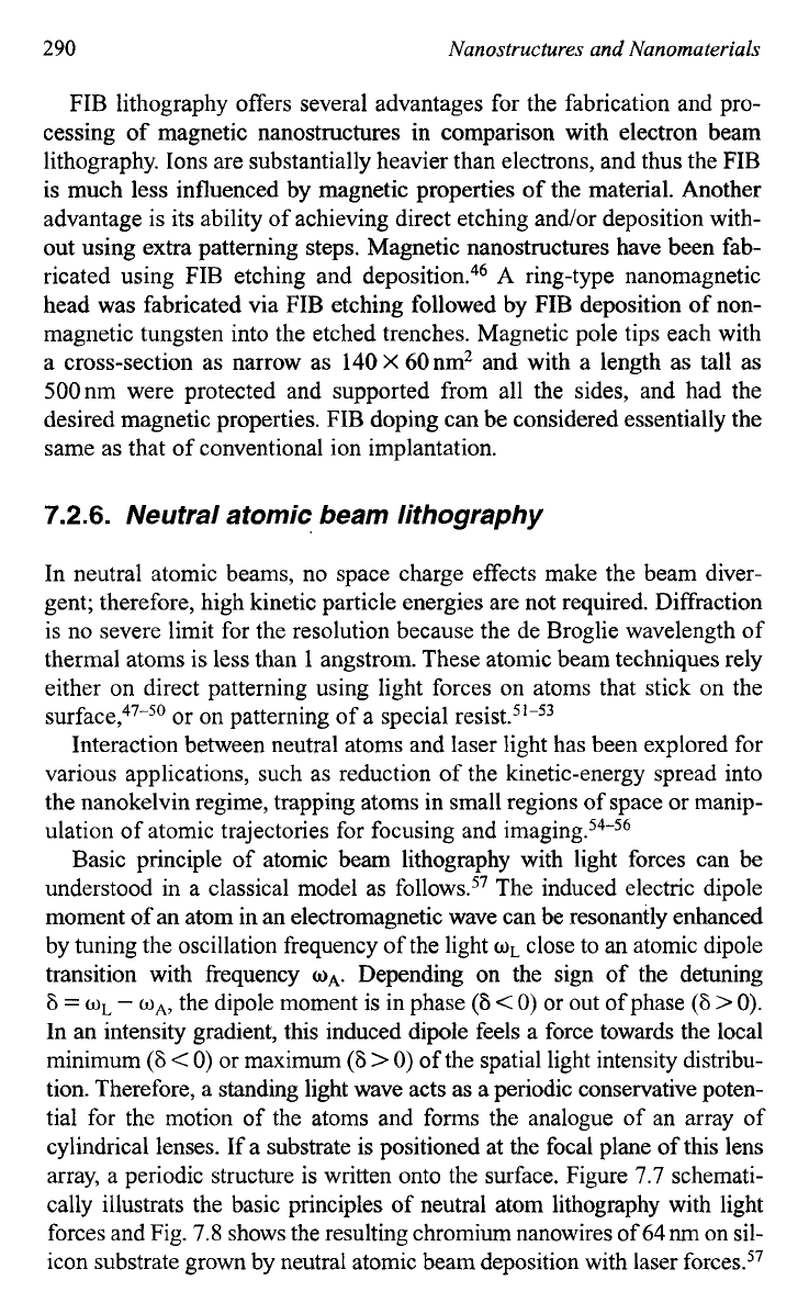
Basic principle of atomic beam lithography with light forces can be
understood in a classical model as follows.57 The induced electric dipole
moment of an atom in an electromagnetic wave can be resonantly enhanced
by tuning the oscillation frequency of the light
oL
close to an atomic dipole
transition with frequency
oA.
Depending on the sign of the detuning
6
=
oL
-
oA,
the dipole moment is in phase
(6
<
0)
or out
of
phase
(6
>
0).
In an intensity gradient, this induced dipole feels a force towards the local
minimum
(6
<
0)
or maximum
(6
>
0)
of the spatial light intensity distribu-
tion. Therefore, a standing light wave acts as a periodic conservative poten-
tial for the motion of the atoms and forms the analogue
of
an array of
cylindrical lenses. If a substrate is positioned at the focal plane of this lens
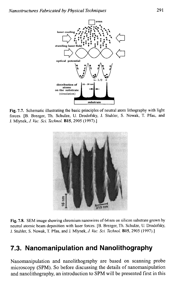
array, a periodic structure is written onto the surface. Figure
7.7
schemati-
cally illustrats the basic principles of neutral atom lithography with light
forces and Fig.
7.8
shows the resulting chromium nanowires of
64
nm
on sil-
icon substrate grown by neutral atomic beam deposition with laser forces.57
Nanostructures Fabricated by Physical Techniques
29
1
optical potential
I-
2.12
-I
atoms
on the substrate
Fig.
7.7.
Schematic illustrating the basic principles of neutral atom lithography with light
forces. [B. Brezger, Th. Schulze,
U.
Drodofsky,
J.
Stuhler,
S.
Nowak,
T.
Pfau, and
J.
Mlynek,
J.
Vac.
Sci.
Technol.
B15,
2905 (1997).]
Fig.
7.8.
SEM image showing chromium nanowires
of
64nm on silicon substrate grown by
neutral atomic beam deposition with laser forces.
[B.
Brezger, Th. Schulze,
U.
Drodofsky,
J.
Stuhler,
S.
Nowak, T. Pfau, and
J.
Mlynek,
J.
Vac.
Sci.
Echnol.
B15,
2905
(1997).]
7.3.
Nanomanipulation and Nanolithography
Nanomanipulation and nanolithography are based on scanning probe
microscopy (SPM).
So
before discussing the details of nanomanipulation
and nanolithography, an introduction to SPM will be presented first in this
292
Nanostructures and Nanomaterials
section.
SPM
differs from other imaging techniques such as scanning
electron microscopy
(SEM)
and transmission electron microscopy
(TEM)
and offers the possibility to manipulate molecules and nanostructures on
a surface.
SPM
consists of two major members: scanning tunneling
microscopy
(STM)
for electrically conductive materials and atomic force
microscopy
(AFM)
for dielectrics. In this section, near-field scanning
optical microscopy and near-field photolithography are also included,
since they share a lot of similarities with
SPM.
7.3.1.
Scanning tunneling microscopy
(STM)
STM
relies on electron tunneling, which is a phenomenon based on quan-
tum
mechanics, and can be briefly explained as follows.58 For more
detailed discussion on the fundamentals, the readers are referred to excel-
lent
book^.^^,^^
Let
us
first consider a situation where
two
flat surfaces of
a metal or semiconductor are separated by an insulator
or
a vacuum as
schematically illustrated in Fig.
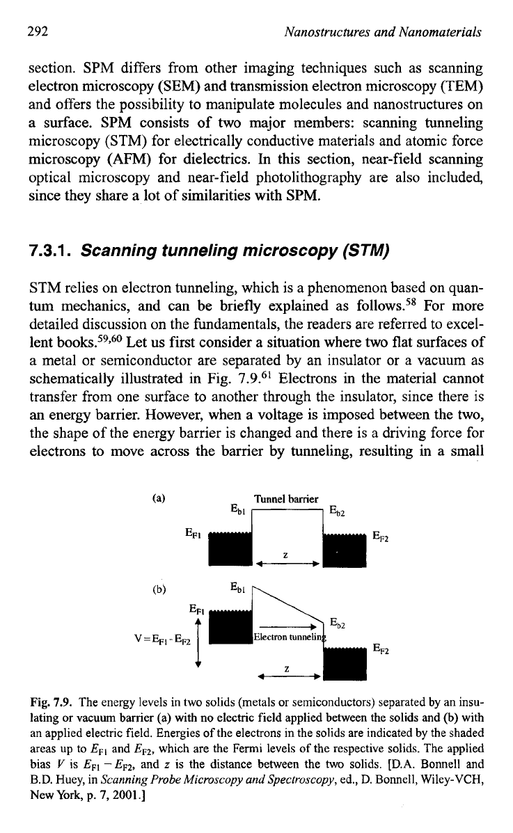
7.9.61 Electrons in the material cannot
transfer from one surface to another through the insulator, since there is
an energy barrier. However, when a voltage is imposed between the two,
the shape of the energy barrier is changed and there is a driving force for
electrons to move across the barrier by tunneling, resulting in a small
(a)
Tunnel
barrier
Fig.
7.9. The energy levels in two solids (metals or semiconductors) separated by an insu-
lating
or
vacuum barrier (a) with no electric field applied between the solids and (b) with
an applied electric field. Energies of the electrons in the solids are indicated by the shaded
areas
up
to
EFI
and
EF2,
which are the Fermi levels
of
the respective solids. The applied
bias
V
is
EF1
-EF2,
and
z
is
the distance between the two solids.
[D.A.
Bonnell and
B.D. Huey, in
Scanning
Probe
Microscopy
and
Spectroscopy,
ed.,
D.
Bonnell, Wiley-VCH,
New
York,
p.
7,2001
.]
Nanostructures Fabricated by Physical Techniques
293
current when the distance is sufficiently small
so
that the electron wave
functions extended from the two surfaces overlap. The tunneling current,
I,
is given by:
Ia
e-2b (7.5)
where
z
is the distance between the
two
metals or the thickness of the insu-
lator and
k
is given by:
2m(V-E)
k=v
h
(7.6)
where
m
is the mass of an electron,
h
is Planck’s constant,
E
is the energy
of electron, and
V
is the potential in the insulator. Similar discussion is
applicable to a tip-planar surface geometry, the configuration of a STM.
However, the tunneling current is then given by:
(7.7)
where
z
is the distance between the tip and the planar surface or sample,
pt
is the tip electronic structure,
ps
is the sample electronic structure, and
C
is a constant dependent on the voltage applied between the tip and the
sample surface. The tunneling current decays exponentially with the tip-
sample distance. For example, a 0.1 nm decrease in the distance will
increase the tunneling current by one order of magnitude. Such a quantum
mechanical property has been utilized in the STM.
In a typical STM, a conductive tip is positioned above the surface of a
sample. When the tip moves back and forth across the sample surface at
very small intervals, the height of the tip is continually adjusted to keep
the tunneling current constant. The tip positions are used to construct a
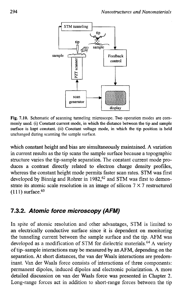
topographic map of the surface. Figure 7.10 schematically depicts a STM
structure. An extremely sharp tip usually made of metals or metal alloys,
such as tungsten or PtIr alloy is mounted on to a three-dimensional posi-
tioning stage made of an array of piezoelectrics. Such a tip would move
above the sample surface in three dimensions accurately controlled by the
piezoelectric arrays. Typically the distance between the tip and the sample
surface falls between
0.2
and 0.6 nm, thus a tunneling current in the scale
of 0.1-lOnA is commonly generated. The scanning resolution is about
0.01 nm in
XY
direction and
0.002
nm in
Z
direction, offering true atomic
resolution three-dimensional image.
STM can be operated in two modes. In constant current imaging, a feed-
back mechanism is enabled that a constant current is maintained while a
constant bias is applied between the sample and tip. As the tip scans over the
sample, the vertical position of the tip is altered to maintain the constant
separation. An alternating imaging mode is the constant height operation in
294
Nanostructures and Nanomaterials
Feedback
Fk]
generator
Fig.
7.10.
Schematic of scanning tunneling microscope. Two operation modes are com-
monly used.
(i)
Constant current mode,
in
which the distance between the tip and sample
surface is kept constant. (ii) Constant voltage mode, in which the tip position
is
held
unchanged during scanning the sample surface.
which constant height and bias are simultaneously maintained.
A
variation
in current results as the tip scans the sample surface because a topographic
structure varies the tip-sample separation. The constant current mode pro-
duces a contrast directly related to electron charge density profiles,
whereas the constant height mode permits faster scan rates.
STM
was first
developed by Binnig and Rohrer in
1982,62
and
STM
was first to demon-
strate its atomic scale resolution in an image of silicon
7
X
7
restructured
(1 1
1)
surface.63
7.3.2.
Atomic force microscopy
(AFM)
In spite of atomic resolution and other advantages, STM is limited to
an electrically conductive surface since it is dependent on monitoring
the tunneling current between the sample surface and the tip. AFM was
developed as a modification of STM for dielectric materials.64
A
variety
of
tipsample interactions may be measured by an
AFM,
depending on the
separation. At short distances, the van der Waals interactions are predom-
inant. Van der Waals force consists of interactions of three components:
permanent dipoles, induced dipoles and electronic polarization. A more
detailed discussion on van der Waals force was presented in Chapter
2.
Long-range forces act in addition to short-range forces between the tip
Nanostructures Fabricated by Physical Techniques
295
and sample, and become significant when the tipsample distance
increases such that the van der Waals forces become negligible. Examples
of such forces include electrostatic attraction or repulsion, current-
induced or static-magnetic interactions, and capillary forces due to the
condensation of water between the sample and tip. Readers are referred to
an excellent book by I~raelachevili~~ for details and insight of interactions
of surfaces and molecules.
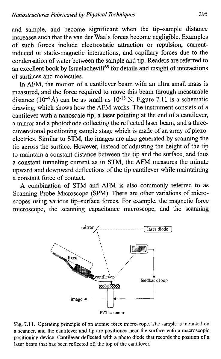
In AFM, the motion of a cantilever beam with an ultra small mass is
measured, and the force required to move this beam through measurable
distance
(104A)
can be as small as
lo-'*
N.
Figure
7.11
is a schematic
drawing, which shows how the AFM works. The instrument consists of a
cantilever with a nanoscale tip, a laser pointing at the end of a cantilever,
a mirror and a photodiode collecting the reflected laser beam, and a three-
dimensional positioning sample stage which is made of an array of piezo-
electrics. Similar to STM, the images are also generated by scanning the
tip across the surface. However, instead of adjusting the height
of
the tip
to maintain a constant distance between the tip and the surface, and thus
a constant tunneling current as in STM, the
AFM
measures the minute
upward and downward deflections of the tip cantilever while maintaining
a constant force of contact.
A
combination of STM and
AFM
is also commonly referred to as
Scanning Probe Microscope
(SPM).
There are other variations of micro-
scopes using various tipsurface forces. For example, the magnetic force
microscope, the scanning capacitance microscope, and the scanning
image
4
I
PZT
scanner
Fig.
7.11.
Operating principle
of
an atomic force microscope. The sample is mounted on
a scanner, and the cantilever and tip are positioned near the surface with a macroscopic
positioning device. Cantilever deflected with a photo diode that records the position
of
a
laser beam that has been reflected
off
the top of the cantilever.