Guozhong Cao. Nanostructures & Nanomaterials: Synthesis, Properties & Applications
Подождите немного. Документ загружается.


276
Nanostructures and Nanomaterials
219. D.W. Murphy, PA. Christian, F.J. Disalvo, and J.V Waszczak,
Inorg.
Chem.
24, 1782
220. R. Clement,
J.
Am. Chem.
SOC.
103,6998 (1981).
221. L.F. Nazar and A.J. Jacobson,
1
Chem.
SOC.
Chem.
Commun.
570 (1986).
222. R. Schollhom,
Physics
of
Intercalation
Compounds,
Springer-Verlag, Berlin, 198 1.
223. R.W. Siegel, S.K. Chang, B.J. Ash,
J.
Stone, PM. Ajayan, R.W. Doremus, and
224. J.P.
Tu,
N.Y. Wang,
Y.Z.
Yang, W.X.
Qi,
F. Liu, X.B. Zhang, H.M. Lu, and
M.S.
Liu,
225. W.V. Kotlensky,
Chem.
Phys.
Carbon
9,
173 (1973).
226.
S.
Vaidyaraman, W.J. Lackey, G.B. Freeman, P.K. Agrawal, and M.D. Langman,
227.
F!
Dupel,
X.
Bourrat, and R. Pailler,
Carbon
33, 1193 (1995).
228. A. Meldrum, R.F. Haglund, Jr., L.A. Boatner, and C.W. White,
Adv.
Muter.
13, 1431
229. W. Caseri,
Macromol.
Rapid Commun.
21, 705 (2000).
(1
985).
L. Schadler,
Scripta Muter.
44, 2063 (2001).
Muter. Lett.
52, 452 (2002).
.I
Muter.
Res.
10,
1469 (1995).
(2001).
Chapter
7
Nanostructures Fabricated by
Physical Techniques
7.1.
Introduction
In the previous chapters, we have discussed various routes for the synthesis
and fabrication
of
a variety of nanomaterials; however, the synthesis routes
applied have been focused mainly on the chemical methods approaches. In
this chapter, we will discuss a different approach: fabrication of nanoscale
structures with various physical techniques. Compared to the general chem-
ical fabrication and processing methods, physical fabrication techniques for
producing nanostructures are derived mainly from the techniques applied for
the fabrication of microstructures in semiconductor industry. Particularly the
hndamentals and basic approaches are mostly based on microfabrications.
In this chapter, the following techniques for the fabrication of nanostructures
and nanopatterns are discussed:
(1)
Lithographic techniques
(a) Photolithography
(b) Phase shifting optical lithography
(c) Electron beam lithography
(d) X-ray lithography
(e) Focused ion beam lithography
(0
Neutral atomic beam lithography
277
278
Nanostructures and Nanomaterials
(2)
Nanomanipulation and nanolithography
(a) Scanning tunneling microscopy (STM)
(b) Atomic force microscopy
(AFM)
(c) Near-field scanning optical microscopy
(NSOM)
(d) Nanomanipulation
(e) Nanolithography
(3)
Soft lithography
(a) Microcontact printing
(b) Molding
(c) Nanoimprint
(d) Dip-pen nanolithography
(4)
Self-assembly of nanoparticles or nanowires
(a) Capillary force induced assembly
(b) Dispersion interaction assisted assembly
(c) Shear force assisted assembly
(d) Electric-field assisted assembly
(e) Covalently linked assembly
(0
Gravitational field assisted assembly
(8)
Template assisted assembly
(5)
Other methods for microfabrication
(a) LIGA
(b) Laser direct writing
(c) Excimer laser micromachining
Although all the above-mentioned processes are discussed in this chapter, not
all methods have the same capability in fabricating nanoscaled structures. In
addition, the hndamentals of various fabrication processes differ signifi-
cantly from each other. Each method offers some advantages over other tech-
niques, but suffers from other limitations and drawbacks. No attempt has
been made to exhaustively list all the methods developed in the literature or
the technical details for fabricating nanostructured devices. Similar to previ-
ous chapters, the attention has been focused mainly on the fundamental con-
cepts and general technical approaches. However, more detailed discussion
has been devoted to
SPM
based nanomanipulation and nanolithography, not
only because the processes are relatively new, but also because they are truly
capable of fabricating nanometer scaled structures and devices.
7.2. Lithography
Lithography is also often referred to as photoengraving, and is the process
of transferring a pattern into a reactive polymer film, termed as resist,
Nunostructures
Fabricated
by Physical Techniques
279
which will subsequently be used to replicate that pattern into an underly-
ing thin film or Many techniques of lithography have been
developed in the last half a century with various lens systems and expo-
sure radiation sources including photons, X-rays, electrons, ions and neu-
tral atoms. In spite of different exposure radiation sources used in various
lithographic methods and instrumental details, they all share the same
general technical approaches and are based on similar fundamentals.
Photolithography is the most widely used technique in microelectronic
fabrication, particularly for mass production of integrated circuit.*
7.2.1.
Photolithography
Typical photolithographic process consists
of
producing a mask carrying
the requisite pattern information and subsequently transferring that
pattern, using some optical technique into a photoactive polymer or pho-
toresist
(or
simply resist). There are two basic photolithographic
approaches:
(i)
shadow printing, which can be hrther divided into contact
printing (or contact-mode printing) and proximity printing, and (ii) pro-
jection printing. The terms “printing” and “photolithography” are used
interchangeably in the literature.
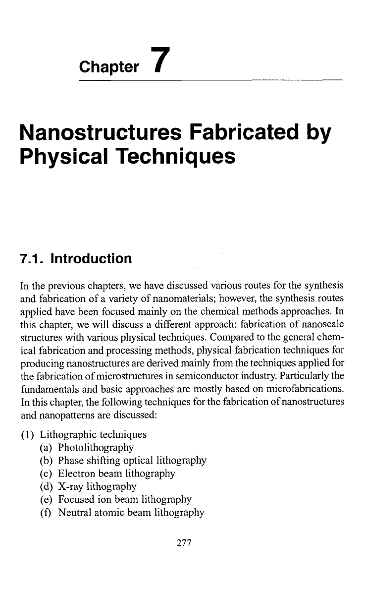
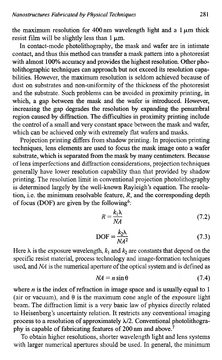
Figure
7.1
outlines the basic steps of the photolithographic process, in
which the resist material is applied as a thin coating over some base and
subsequently exposed in an image-wise fashion through a mask, such that
light strikes selected areas of the resist material. The exposed resist is then
subjected to a development step. Depending on the chemical nature of the
resist material, the exposed areas may be rendered more soluble in some
developing solvent than the unexposed areas, thereby producing a positive
tone image of the mask. Conversely, the exposed areas may be rendered
less soluble, producing a negative tone image of the mask. The effect
of
this process is to produce a three-dimensional relief image in the resist
material that is a replication of the opaque and transparent areas of the
mask. The areas of resist that remain following the imaging and develop-
ing processes are used to mask the underlying substrate for subsequent
etching or other image transfer steps. The resist material resists the etchant
and prevents it from attacking the underlying substrate in those areas
where it remains in place after development. Following the etching
process, the resist is removed by stripping to produce a positive or nega-
tive tone relief image in the underlying substrate.
Diffraction sets the limit
of
the maximum resolution or the minimum
size of the individual elements by photolithography, which can be obtained.
280
Nanostructures and Nanomaterials
,
Resist
Base
llllll
-
-
--Mask
Positive
1
I
Coat
-
Expose
Develop
Etch
-
Strip
-
Fig.
7.1.
Schematic representation
of
the photolithographic process sequences, in which
images in the mask are transferred to the underlying substrate surface.
Diffraction refers to the apparent deviation of light from rectilinear prop-
agation as it passes an obstacle such as an opaque edge and the phenom-
enon of diffraction can be understood qualitatively as follows. According
to geometrical optics, if
an
opaque object is placed between a point light
source and a screen, the edge of the object will cast a sharp shadow on the
screen.
No
light will reach the screen at points within the geometrical
shadow, whereas outside the shadow the screen will be uniformly illumi-
nated. In reality, the shadow cast by the edge is diffuse, consisting of alter-
nate bright and dark bands that extend into the geometrical shadow. This
apparent bending of light around the edge is referred to as diffraction, and
the resulting intensity distribution is called a diffraction pattern.
Obviously diffraction causes the image
of
a perfectly delineated edge
to
become blurred or diffused at the resist surface. The theoretical resolution
capability
of
shadow photolithography with a mask consisting of equal
lines and spaces of width
b
is given by:
where
2b
is the grating period
(1/2b
is the fundamental spatial frequency
v),
s
the gap width maintained between the mask and the photoresist sur-
face,
A
the wavelength of the exposing radiation and
d
the photoresist
thickness. For hard contact printing,
s
is equal to
0,
and from the equation,
Nanostruchtres Fabricated
by
Physical Techniques
28
1
the maximum resolution for 400nm wavelength light and a
1
pm thick
resist film will be slightly less than
1
km.
In contact-mode photolithography, the mask and wafer are in intimate
contact, and thus this method can transfer a mask pattern into a photoresist
with almost
100%
accuracy and provides the highest resolution. Other pho-
tolithographic techniques can approach but not exceed its resolution capa-
bilities. However, the maximum resolution is seldom achieved because of
dust on substrates and non-uniformity of the thickness of the photoresist
and the substrate. Such problems can be avoided in proximity printing, in
which, a gap between the mask and the wafer is introduced. However,
increasing the gap degrades the resolution by expanding the penumbral
region caused by diffraction. The difficulties in proximity printing include
the control of a small and very constant space between the mask and wafer,
which can be achieved only with extremely flat wafers and masks.
Projection printing differs from shadow printing. In projection printing
techniques, lens elements are used to focus the mask image onto a wafer
substrate, which is separated from the mask by many centimeters. Because
of lens imperfections and diffraction considerations, projection techniques
generally have lower resolution capability than that provided by shadow
printing. The resolution limit in conventional projection photolithography
is
determined largely by the well-known Rayleigh’s equation. The resolu-
tion, i.e. the minimum resolvable feature,
R,
and the corresponding depth
of
focus
(DOF)
are given by the following6:
(7.3)
Here
A
is the exposure wavelength,
k,
and
k2
are constants that depend on the
specific resist material, process technology and image-formation techniques
used, and
NA
is the numerical aperture of the optical system and is defined as
NA
=
nsin0
(7.4)
where
n
is the index of refraction in image space and is usually equal to
1
(air or vacuum), and
0
is the maximum cone angle of the exposure light
beam. The diffraction limit is a very basic law
of
physics directly related
to
Heisenberg’s uncertainty relation. It restricts any conventional imaging
process
to
a resolution of approximately
A/2.
Conventional photolithogra-
phy is capable of fabricating features of
200
nm and above?
To
obtain higher resolutions, shorter wavelength light and lens systems
with larger numerical apertures should be used. In general, the minimum
282
Nanostructures and Nanomaterials
feature size that can be obtained is almost the same as or slightly smaller
than the wavelength of light used for the exposure, when a relatively larger
numerical aperture (typically
>0.5)
is used. In such high
NA
lens systems,
the depth of focus becomes very small and
so
the exposure process
becomes sensitive to slight variations in the thickness and absolute posi-
tion of the resist layer.8
Deep Ultra-Violet lithography
(DUV)
based on exposure at wave-
lengths below
300
nm, presents far more difficult technical challenges.
Classical
UV
sources have lower output power in the DUY Excimer lasers
can provide
10
to 20 watts of power at any one of several wavelengths in
the DUV: Of particular interest are the KrCl and
KrF
excimer lasers,
which have outputs at
222
and 249 nm, respectively. High intensity,
microwave powered emission sources provide substantially higher DUV
output than classical electrode discharge mercury lamps9 Light sources
with shorter wavelengths exploited for optical lithography include:
KrF
excimer laser with a wavelength of 249 nm, ArF excimer laser of 193 nm,
F2 excimer laser of 157 nm. With DW, Optical lithography allows one to
obtain patterns with
a
minimal size of -lOOnm.lo~*' Extreme
UV
(EW)
lithography with wavelengths in the range of
11-13
nm has
also
been
explored for fabricating features with even smaller dimensions and is
a
strong candidate for achieving dimensions of 70nm and
be lo^.'^*'^
However,
EUV
lithography meets other problems. The adsorption of light
in this wavelength regime is very strong, and therefore, refractive lens
systems cannot be used. The reflectivity from reflective mirrors is rather
low and, thus, the number of reflective mirrors should be kept
as
low as
possible, not more than six. In addition, an extremely high precision
metrology system is required to make this technique practically viable.I2
Experimentally it is found that when the width of the slit
is
narrower
than the wavelength, the radiation spreads out or is diffracted. Two edges
very close together constitute a slit from which very distinct diffraction
patterns are produced when illuminated with monochromatic light. The
particular intensity distribution observed depends on the distance between
the slit and the screen. For a short distance, the diffraction is Fresnel dif-
fraction, which is the case in shadow printing. For a large distance such as
in projection printing, the diffraction is Fraunhofer diffraction.
In addition to conventional photoresist polymers, Langmuir-Blodgett
films and self-assembled monolayers have been used as resist in photoli-
thography.I4,l5 In such applications, photochemical oxidation, cross-link-
ing, or generation of reactive groups are used to transfer patterns from the
mask to the
mono layer^.'^^'^
Nanostructures Fabricated by Physical Techniques
283
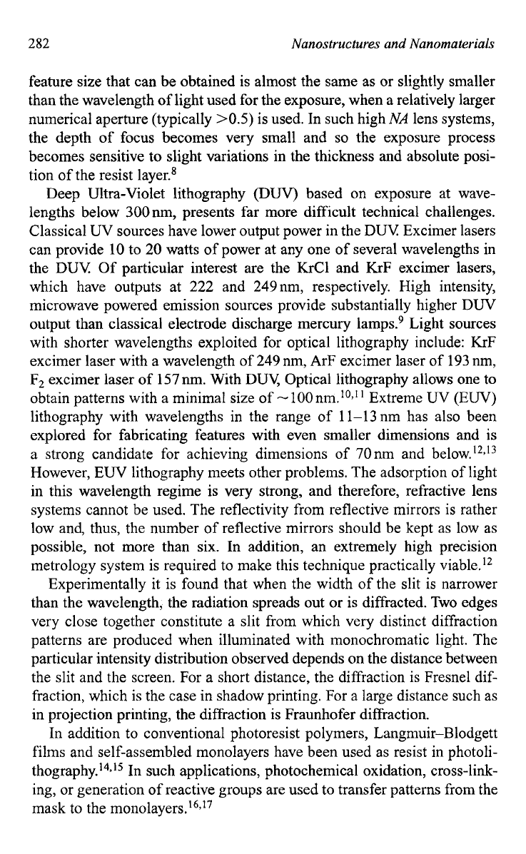
7.2.2.
Phase-shifting photolithography
Phase-shifting photolithography was first developed by Levenson
et
al.
In this method, a transparent mask induces abrupt changes of the phase
of the light
used
for exposure, and cause optical attenuation at desired loca-
tions. These phase masks, also known as phase shifters, have produced
futures of
-
100
nm in photore~ist.'~~~ Figure
7.2
schematically illustrates
the principles of phase-shifting lithography.
A
clear
film,
i.e. a phase shifter
or a phase mask, whose thickness is
A/2(n-
1)
is placed on a photoresist
with conformal contact, the phase angle
of
the exposure light passing
through the
film
shifts by the amount of
T
to the incident light arriving at
the surface of the photoresist. Here
A
is
the wavelength of the exposure
light and
n
is
the index of refraction of the phase mask. Because the light
phase angle
between
the phase shifter and the photoresist is inverted, the
electric field at the phase shifter edge is
0.
So
the intensity of the exposure
light at the surface of the photoresist would
be
zero.
An
image having zero
intensity can
be
formed about the edge of the phase shifter. Phase masks
can be used in both projection and contact-mode photolithographic tech-
niques. For a phase-shifting contact-mode photolithography, there are
two
possible approaches to increase the resolution: (i) reducing the wavelength
of the source of exposure light and (ii) increasing the index of refraction
of
n
b
I
1
I
I
r
Amplitude
at mask
at wafer
Amp'itude
-
O
%
Intensity
at wafer
0
Fig.
7.2.
Schematic illustrating the principles
of
phase shifting lithography, which utilizes
the optical phase change at the phase shifter edge.
2
84
Nanostructures and Nanomaterials
Fig.
7.3. Parallel lines formed in photoresist using near field contact-mode photolithogra-
phy have widths on the order of
100
nm and are
-300
nm in height as imaged
by
(A) AFM
and (B) SEM. [J.A. Rogers,
K.E.
Paul, R.J. Jackman, and G.M. Whitesides,
.J
Vac.
Sci.
Technol.
B16,
59
(1998).]
the photoresist. The achievable photolithographic resolution is roughly of
-Ah/4n,
where
A
is the wavelength of the exposure light and
n
is the refrac-
tive index of the photoresist. Although contact-mode photolithography
with a phase-shifting mask has a higher resolution, conformal contact
between the phase-shifting mask and the photoresist on wafer is difficult to
achieve, due to the presence of dust, non-uniformities in the thickness of
the photoresist, and bowing of the mask or the substrate. However, by intro-
ducing elastomeric phase-shifting masks, conformal contact can be rela-
tively easily achieved and feature lines as narrow as 50nm have been
generated.2’,22 The resolution achieved corresponds approximately to A/5.
An improved approach to conformal near field photolithography is to use
masks constructed from
‘‘soft”
organic elastomeric
polymer^.^^-^^
Figure
7.3
shows a pattern created using such a contact-mode phase-shifting photolith-
ographic process.25
7.2.3.
Electron beam lithography
A finely focused beam of electrons can be deflected accurately and precisely
over a surface. When the surface is coated with a radiation sensitive poly-
meric material, the electron beam can be used to write patterns of very high
resolution.2629. The first experimental electron beam writing systems were
designed to take advantage of the high resolution capabilities in the late
Nunostructures Fabricated by Physical Techniques
285
sixties.30 Electron beams can be focused to a few nanometers in diameter and
rapidly deflected either electromagnetically or electrostatically. Electrons
possess both particle and wave properties; however, their wavelength is on
the order of a few tenths of angstrom, and therefore their resolution is not
limited by diffraction considerations. Resolution of electron beam lithogra-
phy is, however, limited by forward scattering of the electrons in the resist
layer and back scattering from the underlying substrate. Nevertheless, elec-
tron beam lithography is the most powerhl tool for the fabrication of feath-
ers as small as
3-5
nm.31332
When an electron beam enters a polymer film or any solid material,
it
loses energy via elastic and inelastic collisions known collectively as elec-
tron scattering. Elastic collisions result only in a change of direction of the
electrons, whereas inelastic collisions lead to energy
loss.
These scatter-
ing processes lead to a broadening of the beam, i.e. the electrons spread
out as they penetrate the solid producing
a
transverse or lateral electron
flux normal to the incident beam direction, and cause exposure of the
resist at points remote from the point of initial electron incidence, which
in turn results in developed resist images wider than expected. The mag-
nitude of electron scattering depends on the atomic number and density of
both the resist and substrate as well as the velocity of the electrons or the
accelerating voltage.
Exposure of the resist by the forward and backscattered electrons
depends on the beam energy, film thickness and substrate atomic number.
As
the beam energy increases, the energy loss per unit path length and scat-
tering cross-sections decreases. Thus the lateral transport
of
the forward
scattered electrons and the energy dissipated per electron decrease while
the lateral extent of the backscattered electrons increases due to the
increased electron range.
As
the resist film thickness increases, the cumu-
lative effect of the small angle collisions by the forward scattered electrons
increases. Thus the area exposed by the scattered electrons at the resist-
substrate interface is larger in thick films than in thin films. Proper expo-
sure requires that the electron range in the polymer film be greater than the
film thickness in order to ensure exposure of the resist at the interface.
As
the substrate atomic number increases, the electron reflection coefficient
increases which in turn increases the backscattered contribution.
Electron beam systems can be conveniently considered in two broad
categories: those using scanned, focused electron beams which expose the
wafer in serial fashion, and those projecting an entire pattern simultane-
ously onto a wafer. Scanning beam systems can be further divided into
Gausian or round beam systems and shaped beam systems. All scanning
beam systems have four typical subsystems: (i) electron source (gun),