Gersten J.I., Smith F.W. The Physics and Chemistry of Materials
Подождите немного. Документ загружается.

444 CHARACTERIZATION OF MATERIALS
Note that single electron–electron collisions will not produce backscattering, whereas
electron–ion collisions will. At high energies, where core-electron knockout is possible,
it will often be followed by characteristic x-ray emission. Superimposed on this will
be the brehmsstrahlung spectrum due to the rapid deceleration of the electrons. The
energy of the beam spreads out and is deposited over a region ³ 1
µm into the surface.
The easiest electrons to detect are the secondary electrons because they are numerous
and all of low energy. Backscattered electrons are particularly useful because the cross
section for backscattering depends on the atomic number of the target, in accordance
with our understanding of Rutherford scattering. Thus materials with different Z will
produce different amounts of backscattering. This provides a means for contrasting one
type of atom with another.
In the scanning-electron microscope, one may deflect the electron beam so that it
focuses on different parts of the sample. As it rasters over the surface, one detects the
electrons, optical luminescence, or x-rays emitted as a function of the position where
the beam is when these are produced. This often involves the use of a scintillation
counter and photomultiplier tube. The data may be processed and a visual image of
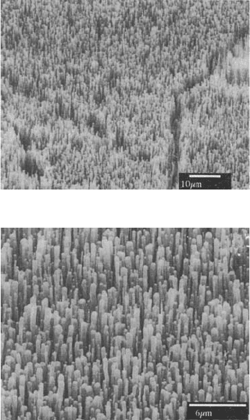
(a)
(b)
Figure W22.16. SEM micrographs of carbon nanotubes on polycrystalline Ni substrates. [From
Z. P. Huang et al., Appl. Phys. Lett., 73, 3845 (1998). Copyright 1998 by the American Institute
of Physics.]
CHARACTERIZATION OF MATERIALS 445
the surface presented. The depth of field and magnification are controlled by varying
the focal lengths. Resolutions ³ 10 nm are achievable.
Instead of gathering the electrons or radiation from the incident surface of the crystal,
it is also possible to use a thin film and gather them from the opposite side of the crystal.
This technique is called scanning-transmission electron microscopy (STEM).
Figure W22.16 illustrates a scanning electron micrograph of highly oriented, multi-
walled carbon nanotubes on a polycrystalline Ni substrate. The nanotubes were grown
by chemical vapor deposition. It is found that growth takes place within the grain
surface but not along the grain boundaries.
W22.13 Transmission-Electron Microscopy
In the transmission-electron microscope (TEM) a thin slice of the material to be studied
(0.1 to 0.5
µm thick) is used and an energetic electron beam (20 to 100 keV) is passed
directly through the sample. One may view either the image of the sample or the
diffraction pattern that is produced on a fluorescent screen. Magnetic lenses are usually
employed because it is possible to achieve short focal lengths with them. A schematic
drawing of the TEM is presented in Fig. W22.17. The filament f heats the needle
like cathode C, which emits electrons thermionically. The beam passes through a hole
(called a wehnelt cap), which causes the beam to converge on and cross the optic axis
(or reach some minimum spot size of radius r
0
c
³ 20 µm for thermionic emitters). The
corresponding point serves as a point source of electrons. The beam is then accelerated
by an anode a and passes through a series of condenser lenses C
i
and apertures A
i
.It
passes through a small portion of the sample and then a series of magnifying lenses
M
i
before it is projected on the fluorescent screen S and recorded on a photographic
plate P. The sample is usually covered with a conductive coating in order to enable it
to discharge electrically.
Typical cathode materials include W and LaB
6
. Their work functions are 4.5 and
2.7 eV, and their operating temperatures are 2800 and ³ 1700 K, respectively. In
some TEMs field emitters are used instead of thermionic emitters. They make use of
Fowler–Nordheim tunneling from very fine cathode tips. Materials used are W and
W covered with ZrO
2
. They may be operated at considerably lower temperatures, so
the thermal spread of electron energies is considerably smaller than the ³ 3eVfor
thermionic emitters. This allows one to obtain a much better minimum spot size (³ 5
to 50 nm). Field-emission sources are brighter than thermionic sources. The respec-
tive brightnesses are typically ³ 10
9
and ³ 10
12
A/m
2
Ð steradian. Typical vacuums
for thermionic-emitter systems range from 10
2
to 10
4
Pa. For field-emitter systems
ultrahigh vacuums are established, typically in the range 10
7
to 10
8
Pa.
sample
fcwa
C
1
A
1
C
2
A
2
A
3
M
1
M
2
M
3
S
p
Figure W22.17. Schematic view of a transmission-electron microscope.

446 CHARACTERIZATION OF MATERIALS
The focal length of a magnetic lens is given by the formula
1
f
D
e
8mV
1
1
B
2
z dz, W22.87
where Bz is the magnetic field along the axis and eV is the energy of the electron
as it passes through the lens. The magnetic lens also rotates the image by an angle
given by
D
e
8mV
1
1
Bz dz. W22.88
The magnetic lenses have aberrations associated with them. These include the impor-
tant spherical aberrations, chromatic aberrations, and astigmatism, as well as the less
important coma and barrel or pincushion distortions. Spherical aberrations are due the
fact that the rays scattered from an object point at small angles ˇ through the lens are
focused at a different image point than rays scattered at larger angles. The net result
is that an object point along the axis is imaged to a disk of radius r
s
rather than to a
point. It may be shown that the size of this disk is given by the formula r
s
D C
s
ˇ
3
,
where C
s
is ³ 1 mm. Unlike in the optical-lens case, there is no simple way to correct
for spherical aberrations.
Chromatic aberrations are due to a variation of focal length with beam energy,
and may be understood in terms of Eqs. (W22.87) and (W22.88). Inelastic losses of
V ³ 5 to 50 eV are common for electrons passing through the sample, due to the
excitation of electron–hole pairs, plasmons, phonons, and so on. The net result is that
an object point is imaged to a disk-of-confusion whose radius is r
c
. It may be shown
that r
c
D C
c
ˇV/V,whereC
c
is a distance characterizing the axial variation of the
magnetic field in the lens.
The imprecision with which magnetic lenses can be constructed leads to asymmetries
being present. Astigmatism is caused by having a different focal length for electrons
deflected in the x direction than in the y direction, the difference being f
A
. A point
source is focused to a disk of minimum size r
A
D ˇf
A
. It may usually be corrected
by employing a balancing astigmatic lens.
The Rayleigh diffraction criterion gives an estimate for the minimum separation of
two resolvable points, r
d
D 0.61(/ˇ,where( is the wavelength of the electrons. One
may obtain an estimate for the instrument resolution by assuming that the spherical
aberration and diffraction dominate. Then
rˇ D
0.61(
ˇ
2
C C
s
ˇ
3
2
.W22.89
There is a competition between the diffraction of the beam and the spherical aberrations
of the lenses. The minimum value of r occurs when ˇ D 0.61(/C
s
p
3
1/4
and its
value is r
min
D 0.91C
1/4
s
(
3/4
. The smaller ( can be made, the better the resolution
will be. Typical optimal instrumental resolutions are of the order of several tenths of a
nanometer. For 100-keV beams r D 0.33 nm is possible, but the samples must be less
than 5 nm in thickness. For 400-keV beams, a resolution of 0.17 nm has been obtained.
By using beams of incoherent rather than coherent electrons and by underfocusing the
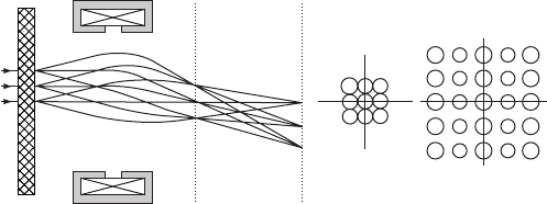
CHARACTERIZATION OF MATERIALS 447
Image
plane
Diffraction
spots
Image
points
Sample
Back
focal
plane
Image
plane
Back
focal
plane
x
y
z
Figure W22.18. A forward-directed beam and diffracted beams are produced when the incident
electron beam passes through the sample. The right figures show the diffraction spots in the
back focal plane and the sample image points in the image plane.
electron beam to compensate partially for spherical aberrations, it has recently been
possible to obtain 0.078-nm resolution with a 300-keV electron beam.
†
After passing through the sample, the diffraction spots create images on the back-
focal plane of the object lens (e.g., C
2
of Fig. W22.17). One may use the magni-
fying lenses to view this diffraction pattern directly on the screen and to produce a
transmission-electron diffraction (TED) micrograph. Alternatively, a real image of the
sample is produced on the image plane of the object lens. This real image may be
magnified and projected on the fluorescent screen.
Emerging from the sample is both a forward-directed transmitted beam of electrons
and diffracted beams of electrons, as illustrated in Fig. W22.18. The aperture A
3
of
Fig. W22.17 may be used to choose one or more of these beams selectively and block
the others. The technique is called selective-area diffraction (SAD). In the method of
bright-field (BF) imaging one allows the forward-directed beam to be imaged on the
screen. In the method of dark-field (DF) imaging, a diffracted beam is selected instead.
The diffraction pattern in the back-focal plane and the image of the sample are depicted
in the right-hand side of Fig. W22.18. The central diffraction spot corresponds to the
forward-directed beam. The other spots correspond to various diffracted beams for a
case where there is fourfold symmetry. As will be seen in Section W22.14, the more
beams that are accepted by the aperture, the higher the resolution will be.
Kikuchi Lines. Diffraction of electrons differs from that of x-rays in two important
respects. First, the samples are thin, so there are only a finite number of atomic layers,
N
z
, perpendicular to the beam. Second, inelastic processes are much more important
for electrons than for x-rays.
Due to the finite value of N
z
³ 1000, instead of there being a pure spot diffraction
pattern, the spots are elongated into streaks of length G
z
³ 2/N
z
d,whered is the
lattice spacing. Thus it is still possible to see a diffraction spot even when the von
Laue condition is not exactly satisfied. One defines the mismatch reciprocal vector s
†
P. D. Nellist and S. J. Pennycook, Phys. Rev. Lett., 81, 4156 (1998).

448 CHARACTERIZATION OF MATERIALS
z
G
∆
G
z
s
k
k'
2q
Ewald sphere
Figure W22.19. Ewald sphere and streaking of diffraction spots.
through the relation k
0
k D G C s. This is illustrated in Fig. W22.19. The vectors k
and k
0
,makinganangle2 with each other, have a common origin and have the same
length. The head of vector k touches the origin of reciprocal-lattice space. The Ewald
sphere passes through this origin. A diffraction spot will still be produced if the head
of vector k
0
also touches the Ewald sphere, but is located a distance s G
z
in the
z direction away from the nearest reciprocal lattice point, G. The extent of G
z
is
denoted by the dashed rectangle in the figure.
Suppose the electron is incident on the lattice in a direction that is far removed from
satisfying the von Laue diffraction condition. Electrons can suffer inelastic collisions,
thereby losing energy and scattering into various directions centered around the incident
direction. Energy losses of up to 50 eV are common. The probability for scattering
through a given angle relative to the forward direction falls rapidly with increasing
angle. An effect of this is illustrated in Fig. W22.20, where an electron suffers an
inelastic collision at point p. For some scattered beams the energy and direction will
be just right to satisfy the Bragg diffraction condition for a set of lattice planes. Two
such planes L and L
0
are illustrated in Fig. W22.20. The beams B and B
0
are able
q
q
q
q
p
L
L'
B'
C'
C
B
k
Figure W22.20. Formation of Kikuchi lines by Bragg diffraction and constructive interference
of beams of inelastically scattered electrons.
CHARACTERIZATION OF MATERIALS 449
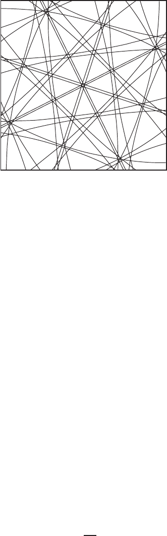
Figure W22.21. Kikuchi line pattern. (Generated using the computer program KOQUA2.2
written by S. Weber and C. Schetelich.)
to interfere with each other, as are the beams C and C
0
. If the Bragg condition is
satisfied for the direction of beams B and B
0
, a bright spot will be produced in that
direction. The intensity comes at the expense of radiation that was in the near-forward
direction, so there will be a corresponding dark spot established along the direction
of beams C and C
0
. The angular spread between the lines C and B is 2, independent
of the angles through which the electrons are scattered. When one takes into account
all possible angles of incidence for the electrons, the beams B and C sweep out the
surfaces of cones. These cones intersect the projection of the Ewald sphere in a pair
of hyperbolas. For high-energy electrons the radius of the Ewald sphere is large and it
looks approximately planar. The intersections of the cones with the plane then produce
a pair of approximately parallel lines. This gives rise to the Kikuchi line pattern.To
each set of lattice planes there is a pair of Kikuchi lines, one dark and one bright.
Furthermore, these lines are parallel to the intersection of the corresponding lattice
planes with the Ewald sphere.
The Kikuchi line pattern shifts if the crystal is tilted. This permits one to orient a
crystal precisely. An example of a Kikuchi line pattern, together with a set of diffraction
spots, is illustrated in Fig. W22.21. Furthermore, at the intersection of Kikuchi lines,
one finds spot patterns. Thus the Kikuchi patterns are used as maps to locate the
orientations of the crystal, which give rise to diffraction-spot patterns.
W22.14 High-Resolution Transmission-Electron Microscopy
In high-resolution transmission-electron microscopy (HRTEM) a beam of high-energy
electrons is passed through a thin sample and focused on an image plane. Suppose that
the sample is a crystal. Recall that the diffraction condition is
G
· k C
G
2
2
D 0.W22.90
If k is much larger than G, this equation can be satisfied only for those lattice planes
whose G vectors are almost perpendicular to k, for that is the only way to keep the
450 CHARACTERIZATION OF MATERIALS
magnitude of the first term comparable to that of the second term. The angles between
k and k
0
are given by
sin D
G
2k
W22.91
and will be small.
As mentioned earlier, magnetic lenses have associated with them spherical aberra-
tions. A beam far from the optical axis will not focus at the same point as a beam
near the optical axis. In conventional microscopy, therefore, it is usually not possible
to focus the Bragg-reflected beams along with the directly transmitted beam. This puts
a limitation on the resolution. However, in HRTEM the Bragg peaks are coming off at
small angles and therefore remain paraxial (i.e., close to the optic axes). The spherical
aberrations are therefore not of major concern and it is possible to focus several Bragg
orders together (Fig. W22.22).
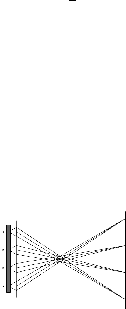
In the figure, the sample is labeled S, the lens, L, the focal plane, F, and the image
plane, I. An electron beam is incident on the sample from the left and is focused on
the image plane. Note that the various Bragg-reflected beams combine with the direct
beam in the image plane. This causes a sharply defined focal spot. The reason for
this is that slightly away from the focal spot the various beams start to interfere with
each other destructively and the intensity decays rapidly with distance away from the
spot. The more diffracted beams that can be collected, the sharper the image. Once
the image is formed on the image plane, further magnification is possible by the use
of additional lenses, as in the case of TEM.
The angular sharpness of the image varies inversely as the number of diffracted
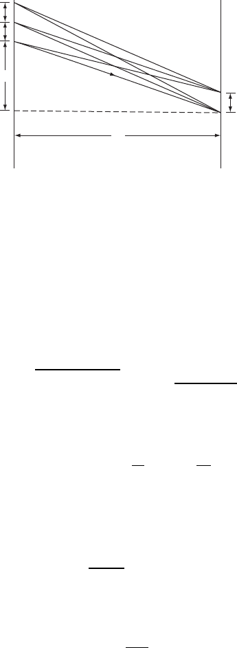
beams in a given direction that may be focused. This is illustrated with a two-
dimensional example. Consider Fig. W22.23, in which a set of N beams passes through
the lens at positions y
i
and is focused at the lower point on the screen. At this point
all the beams arrive in phase with each other:
D
i
C kl
i
,iD 1,...,N, W22.92
LSFI
Figure W22.22. A large number of diffracted beams are focused by the lens L and are combined
to form a high-resolution image of the sample S on the image plane I.
CHARACTERIZATION OF MATERIALS 451
3
2
1
Lens Screen
D
L'
1
L
1
y
1
∆
∆
y
Figure W22.23. Estimation of the angular sharpness of the image.
where the
i
C kl
i
differ by integer multiples of 2. The total amplitude at the point
is therefore
A D
N
iD1
expi D N expi . W22.93
Next consider a point on the screen a distance y above the original point. The phase
that each beam arrives with is now different:
i
D
i
C k
y
i
y
2
C D
2
' k
yy
i
y
2
/2
D
,W22.94
where it is assumed that D is much larger than y
i
. The amplitude at the upper point is
therefore
A
0
D
N
nD1
exp
i
ik
D
yy
n
y
2
2
.W22.95
The points y
n
on the lens are separated from each other by an arbitrary distance .
This amplitude will fall to zero when the phases are spread uniformly over a circle,
that is, when
kyN
D
D 2, W22.96
which shows that y is inversely proportional to N:
y D
(D
N
.W22.97
In the three-dimensional case the diffracted beams will be spread out over an area.
The total number of beams will be denoted by N
2
. Thus the size of the image falls off
as the inverse of the square root of the number of focused diffracted beams.
It is now possible to use HRTEM to obtain spatial resolution approaching 0.1 nm,
if beams of 1 MeV are used, although most conventional HRTEM applications use
lower-energy beams and settle for more modest resolution goals. It is an ideal tool for
studying line defects, planar defects, and interfaces.
452 CHARACTERIZATION OF MATERIALS
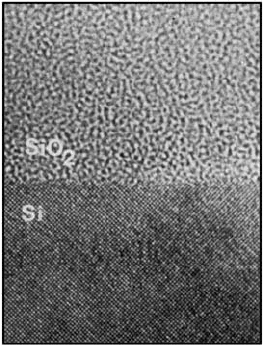
Figure W22.24. HRTEM image of the Si/a-SiO
2
interface. (From J. M. Gibson, High resolution
transmission electron microscopy, Mater. Res. Soc. Bull., Mar. 1991, p. 27.)
An HRTEM image of a Si/a-SiO
2
interface is shown in Fig. W22.24. The individual
atoms of the Si crystal appear in the lower half of the image. The upper half shows
the image of the amorphous silica.
W22.15 Low-Energy Electron Microscopy
Like LEED, low-energy electron microscopy (LEEM), involves forming a diffraction
pattern using elastically scattered electrons from a crystalline surface. Unlike LEED,
however, most of the pattern is discarded. Usually, one diffracted beam is extracted and
imaged on a screen using conventional electron-microscope lenses. Typical energies
used are in the range 100 eV to 3 keV. The resolution is as fine as 2 nm. LEEM is
useful for seeing structure on a mesoscopic size scale. This includes surface steps,
dislocations, imperfections, islands of adsorbates, superlattice structure, grains, and
surface inhomogeneity.
In LEEM the electron beam is directed at the sample with near-normal incidence.
Electrons are emitted from an electron gun from an oblique direction to the surface,
and a bending magnet is used to change the direction to normal incidence. The same
bending magnet is used to redirect the reflected electrons in another oblique direction
toward the image plane. In Fig. W22.25 the basic imaging scheme is displayed for the
case where LEEM is used to image a surface step, S, on the left. For simplicity the
injection, bending magnet, and extraction are not shown, and it is simply assumed that
the electron beam is incident from the right. Four reflected beams are illustrated, each
with a pair of diffracted beams. The beams pass through an electron lens, L, and then
through a screen, A, with an aperture in it. The aperture is placed in the focal plane
of the lens. Only the specularly reflected rays are allowed through, the other diffracted
beams are blocked. The rays that pass through the aperture illuminate the screen I. In
passing through the aperture, the beams undergo Fresnel diffraction and are broadened
into cones. Thus beam 1 is spread into cone 1, beam 2 into cone 2, and so on. The
regions illuminated by these cones are denoted 1
0
,2
0
, and so on.
CHARACTERIZATION OF MATERIALS 453
1'
2'
D
1
2
3
3'
4'
4
ALS
I
Figure W22.25. Optics of the formation of a LEEM image.
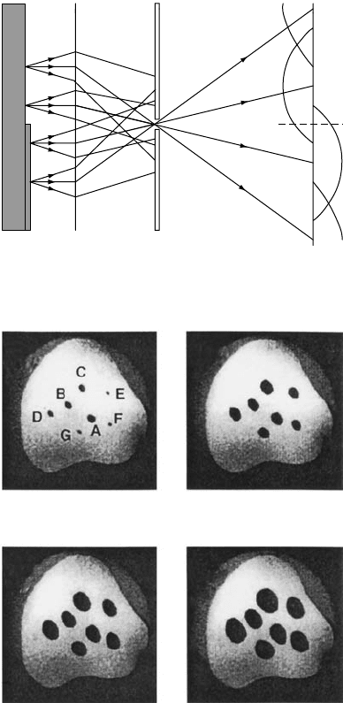
(a) (b)
(c) (d)
Figure W22.26. LEEM micrograph of the etching of a terrace on Si(100) by oxygen at
T D 1235 K. The images are those of vacancy islands at (a)1s,(b)10s,(c)20s,and(d)30
s after nucleation. [From J. B. Hannon et al., Phys. Rev. Lett., 81, 4676 (1998). Copyright 1998
by the American Physical Society.]
The figure illustrates the situation where rays 1 and 2 are reflected from the part of
the step closer to the lens, while rays 3 and 4 come from the part farther from the lens.
Positive amplitude is indicated to the left of the image plane and negative amplitude
to the right of the image plane. Suppose that the energy of the electrons is adjusted so
that the step size is one-fourth of a wavelength. This would cause rays 1 and 2 to be
half a wavelength out of step with rays 3 and 4 when they hit the image plane, I. At