Fahlman B.D. Materials Chemistry
Подождите немного. Документ загружается.

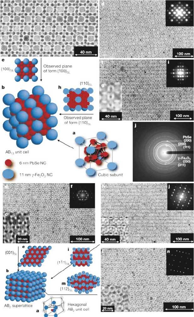
Figure 6.60. Top: TEM micrographs and sketches of AB
13
superlattices (isostructural with intermetallic
phase NaZn
13
) of 11-nm g-Fe
2
O
3
and 6-nm PbSe NCs. Bottom: TEM micrographs and sketches of AB
2
superlattices (isostructural with intermetallic phase AlB
2
) of 11-nm g-Fe
2
O
3
and 6-nm PbSe NCs.
Reproduced with permission from Redi, F. X.; Cho, K. -S.; Murray, C. B.; O’Brien, S. Nature 2003,
423, 968. Copyright 2003 Nature Publishing Group.
528 6 Nanomaterials
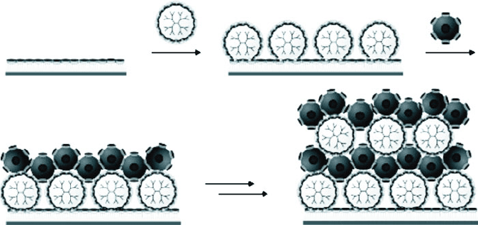
The most popular method used to achieve 3-D arrays such as layered nanostructural
thin films, is the layer-by-layer (LbL) self-assembly pioneered by Decher in the early
1990s.
[170]
This technique is based on the sequential adsorption of species with
complimentary functional groups (e.g., ionic charges) on a variety of substrates.
There are many device applications for LbL thin films, such as self-cleaning surfaces,
surface deactivation of warfare agents, solar energy, drug delivery, and optoelectron-
ics. An interesting recent precedent for LbL nanostructural film growth uses sequential
layering of cyclodextrin-stabilized Au nanoparticles and adamantyl-terminated
dendrimers (Figure 6.61).
[171]
The film thickness was reported as 2 nm per bilayer,
allowing for strict control over the resultant film thickness.
6.3.2. One-Dimensional Nanostructures
The second class of nanoscale building blocks, referred to as 1-D nanostructures, is
reserved for those materials that have nanoscale dimens ions that are equivalent
in all but one direction. Recall that a 0-D nanostructure is analogous to the period
following this sentence (length ¼ width); a 1-D nanostructure is analogous to the
number “1” (length > width).
Since we began the discussion of 0-D nanostructures with nomenclature, we will
follow suit in this section. Once again, it is easy to be confused by the common
synonymous use of the terms nanotube, nanofiber, nanowire, and nanorod. However,
if you think of the analogous bulk materials without the prefix “nano,” there should
be no ambiguity regarding the proper use of these descriptors (Figure 6.62). The
common thread among all of these structures is that their diameters must be within
the 1–100 nm range; typically, their lengths are within the micron (or larger) regime.
Figure 6.61. Illustration of LbL growth of cyclodextrin-stabilized Au nanoparticles (dark spheres) and
adamantyl-terminated PPI dendrimers. Reproduced with permission from Crespo-Biel, O.; Dordi, B.;
Reinhoudt, D. N.; Huskens, J. J. Am. Chem. Soc. 2005, 127, 7594. Copyright 2005 American Chemical
Society.
6.3. Nanoscale Building Blocks and Applications 529
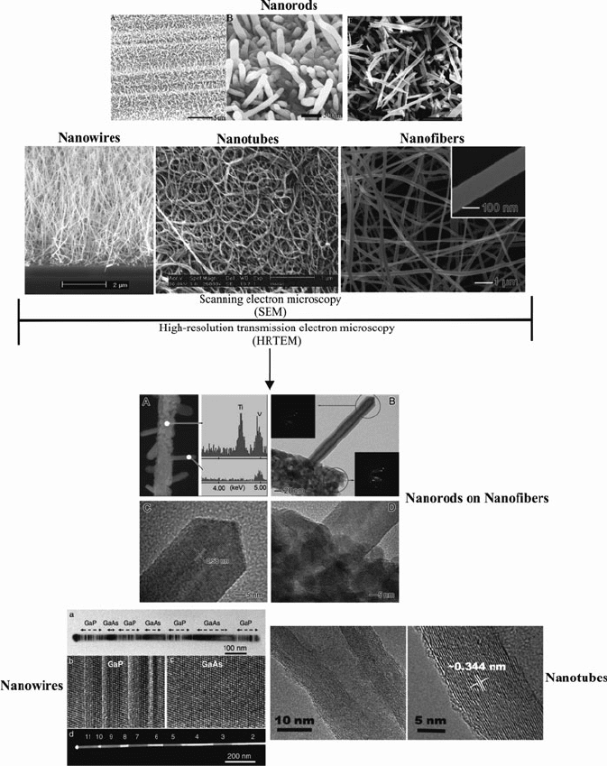
Figure 6.62. Classifications of 1-D nanostructures. The top portion shows SEM images of various
nanostructures.
[172]
Whereas the morphology of nanowires, nanotubes, and nanofibers look identical by
SEM, nanorods are notably different, with much shorter lengths and straight sidewalls. The bottom
portion shows high-resolution TEM images, which provide morphological details of the
nanostructures.
[173]
The top TEM image shows crystalline nanorods grown on the surface of amorphous
nanofibers. The bottom two TEM images illustrate the difference between nanowires/nanotubes – the
latter contains a hollow core. It should be noted that crystalline nanorods may also be termed
“nanocrystals,” as their morphology resembles that of needle-like bulk crystallites.
530 6 Nanomaterials

A nanotube is a 1-D structure that contains a hollow core, whereas the other three
nanoarchitectures are solid throug hout. The term nanofiber should be reserved for
1-D nanostructures that are amorphous (and usually nonconductive) such as poly-
mers and other non-graphitized carbonaceous structures. By contrast, a nanowire
designates a structure that is crystalline, with either metallic or semiconductive
electrical properties.
A nanorod is typically a crystalline 1-D nanostructure, with an overall length
comparable to its width (i.e., both dimensions are < 100 nm). As their name implies,
another feature of nanorods is their rigid sidewall structures. However, since crystalline
nanorods exhibit the same overall shape as needle-like bulk crystals, the term “nano-
crystal” is probably more appropriate for these structures (or, more explicitly: “rod-like
nanocrystals”). Whereas nanowires, nanofibers, and nanotubes exhibit an interwoven
array, nanorods are completely linear in morphology. As such, nanorods are capable of
stacking onto each other to yield interesting 2-D and 3-D arrays – not usually as easy to
perform with the “spaghetti-like” morphology of the other 1-D nanostructures.
Carbon nanotubes (CNTs)
Without questio n, the most widely studied 1-D nanomaterial is the carbon nanotube
(CNT). These structures were first discovered by Iijima in 1991,
[174]
and may be
thought of as a graphitic sheet(s) of sp
2
hybridized carbon atoms (i.e., graphene
[175]
)
rolled into a tubular array. Based on the layers of graphene sheets that comprise the
CNT, the structures are designated as single-walled, double-walled, or multiw alled
nanotubes (SWNTs, DWNTs, or MWNTs, respectively – Figure 6.63). The dia-
meters of CNTs range from 1 nm (SWNTs) to >30 nm (MWNTs), with aspect ratios
(length:width) ranging from 100 to greater than 1 10
6
. Even though the diameters
of CNTs are orders of magnitude smaller than a human hair, their tensile strength is
ca. 20 times greater than steel – a property attributed to extremely strong sp
2
bonding between neighboring hexagonal units.
[176]
The electrical conductivity of SWNTs may vary from metallic to semiconducting,
depending on the way a graphene sheet is folded (Figure 6.64). In particular, the
diameter and helicity of a SWNT are uniquely characterized by the chirality vector
(or Hamada vector),
~
C, which connects crystallographically equivalent graphene
lattice sites. Vector indices designated by (n, m) are used to indicate the direction
and length of the chirality vector (Eq. 21). Equation 22 provides a formula to
calculate the diameter, D,ofa(n, m) nanotube, and Eq. 23 is the relation to
determine the chirality angle, f. When n ¼ 0, the SWNT is denoted as the zigzag
conformation; when n ¼ m, the SWNT is in its armchair form. For all values in
between these extremes, the nanotubes are designated simply as chiral .
~
C ¼n
~
a
1
þm
~
a
2
ð21Þ
D¼
ffiffiffiffiffiffiffiffiffiffiffiffiffi
3d
CC
p
p
ffiffiffiffiffiffiffiffiffiffiffiffiffiffiffiffiffiffiffiffiffiffiffi
n
2
þnmþm
2
p
ð22Þ
6.3. Nanoscale Building Blocks and Applications 531
cos f ¼
2n þ m
2
ffiffiffiffiffiffiffiffiffiffiffiffiffiffiffiffiffiffiffiffiffiffiffiffiffiffiffiffi
n
2
þ m
2
þ nm
p
ð23Þ
where n, m are the integers denoting the number of unit cell vectors along two
directions in the crystal structure of graphene,
~
a
1
;
~
a
2
are the graphene unit cell
vectors, and d
C–C
is the C—C bond length (1.41–1.44 A
˚
).
For metallic SWNTs, the electrical conductance may exceed silver or copper by
three orders of magnitude. Calculations have shown that (n, 0) or zigzag SWNTs
exhibit metallic conductivity when n/3 is an integer, and semiconducting properties
for all other values of n. Similarly for chiral SWNTs, when (2n + m)/3 is an integer ,
the tubes are metallic (otherwise are semiconducting). Finally, armchair SWNTs,
with n ¼ m, exhibit metallic conductivity (Figure 6.65). Most importantly, elec-
tronic band structure calculations show that metallic and semiconducting CNTs are
dependent only on (n, m) – that is, slight structural variations result in dramatic
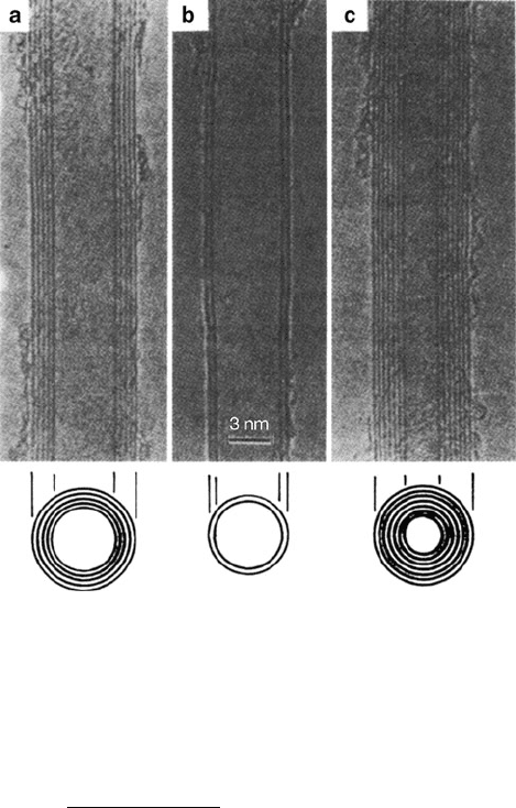
Figure 6.63. TEM images of MWNTs, formed from the folding (a) 5-, (b) 2- (i.e., DWNT), and
(c) 7-stacked graphene sheets. The spacing between individual concentric cylinders is 0.34 nm – the
distance between adjacent planes in graphite. Reprinted from Dresselhaus, M. S.; Dresselhaus, G.;
Eklund, P. C. Science of Fullerenes and Carbon Nanotubes. Copyright 1996, with permission from
Elsevier.
532 6 Nanomaterials
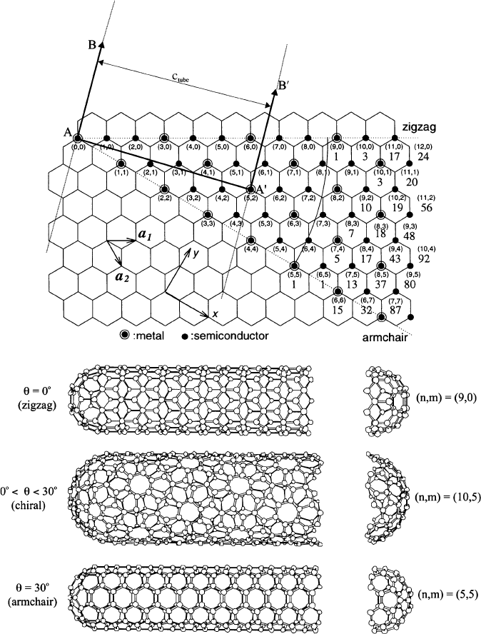
Figure 6.64. Illustration of the honeycomb 2-D graphene network, with possible unit cell vector indices
(n, m). The dotted lines indicate the chirality range of tubules, from y ¼ 0
(zigzag) to y ¼ 30
(armchair). For y values between 0 and 30
, the formed tubules are designated as chiral SWNTs. The
electrical conductivities (metallic or semiconducting) are also indicated for each chiral vector. The
number appearing below some of the vector indices are the number of distinct caps that may be joined
to the (n, m) SWNT. Also shown is an example of how a (5, 2) SWNT is formed. The vectors AB and
A
0
B
0
, which are perpendicular to the chiral vector (AA
0
) are superimposed by folding the graphene sheet.
Hence, the circumference of the SWNT becomes the distance between AB and A
0
B
0
axes. Reprinted from
Dresselhaus, M. S.; Dresselhaus, G.; Eklund, P. C. Science of Fullerenes and Carbon Nanotubes.
Copyright 1996, with permission from Elsevier.
6.3. Nanoscale Building Blocks and Applications 533
changes in their electronic properties. For example, the bandgap of semiconducting
SWNTs may be fine-tuned from ca. 10 meV to 1 eV – with no required addition of
dopants, unlike bulk Si counterparts (Eq. 24). If semiconducting nanotubes exhibit
the same chirality, the bandgap is inversely proportional to the diameter, D (e.g.,
E
g
(7, 0) > E
g
(10,0)). The density of states (DOS) for SWNTs exhibit sharp
maxima, which are known as van Hove singularities resulting from quantum
confinement in directions perpendicular to the tube axis. Optical transitions are
possible between these maxima, which may be observed by Raman spectroscopy
(Figure 6.66).
[177]
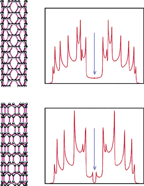
Armchair nanotube
Zigzag nanotube
(5,5)
(7,0)
metal
Semi-
conductor
Density of States
−10.0 −5.0 0.0 5.0 10.0
Energy (eV)
Density of States
−10.0 −5.0 0.0 5.0 10.0
Ener
g
y (eV)
a
b
Figure 6.65. Comparison of the density of states, and resultant electronic properties of armchair and
zigzag SWNTs. Reproduced with permission from Charlier, J.-C. Acc. Chem. Res. 2002, 35, 1063.
Copyright 2002 American Chemical Society.
534 6 Nanomaterials
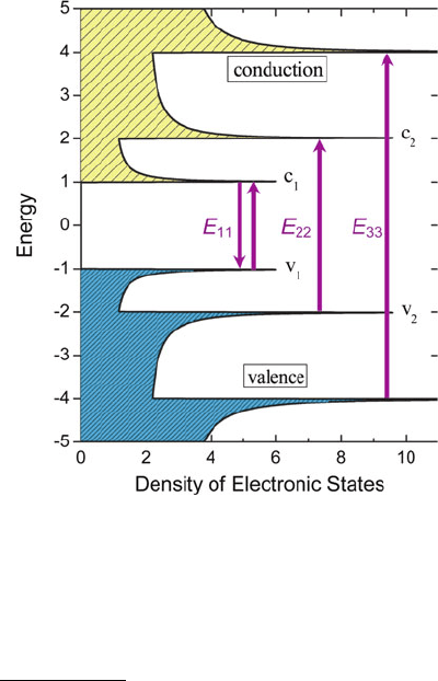
E
g
¼
3:13 eV ðd
cc
Þ
D
ð24Þ
The tunable electronic properties of CNTs are being explored for next-generation IC
architectures. As you may recall from Chapter 4, traditional Si-based microelec-
tronic devices will likely reach a fundamental limit within the next decade or so,
necessitating the active search for replacement materials. Accordingly, an area of
intense investigation is molecular electronics – in which the electronic device is
built from the placement of individual molecules.
[178]
Not surprisingly, the inter-
connects of these devices will likely be comprised of CNTs and other (semi)
conductive 1-D nanostructures such as nanowires.
Since CNTs have a high electrical conductivity and contain sharp tips, these
nanomaterials are the best-known field-emitter
[179]
of any material to date. In
general, the smaller the radius of curvature of the tip, the more concentrated the
electric field will be, which corresponds to increased fie ld emission at low required
voltages. This property is currently being exploited for the design of flat-panel
field emission displays. Though plasma and LCD displays are hot ticket items
at electronics stores, they both possess inherent disadvantages. Plasma displays
are extremely heavy, consume a significant amount of energy, and are prone to
Figure 6.66. Density of states in a semiconducting single-walled carbon nanotube. The sharp maxima
are van Hove singularities. The dominant optical absorption/emission transitions are indicated by arrows.
Reproduced with permission from Weisman, R. B.; Subramoney, S. Electrochem. Soc. Interface, Summer
2006, 42.
6.3. Nanoscale Building Blocks and Applications 535
“burn-in,” which permanently degrades the screen. On the other hand, LCD screens
are expensive to produce and often lack the response time required to view
fast-paced sporting events/movies without blur. In contrast to popular belief, the
new ‘LED TVs’ available at the high end of the HDTV market are not truly LEDs.
These displays are in fact LCDs that simply use LEDs instead of cold cathode
fluorescent lamps as the backlight; in contrast, true LED TVs would not require a
backlight, since each LED pixel would be self-illuminating.
[180]
Hence, as far as
picture quality is concerned, traditional CRT displays are still among the finest
quality. The replacement of this technology with CNTs is a logical step in the
evolution of display panels. Rather than a single electron gun, CNT-based screens
will contain a separate nanotube electron gun for each indivi dual pixel in the
display – dramatically enhancing the resolution and clarity of the picture. Further,
in contrast to current large flat-panel televisions, the overall weight of CNT-based
analogues will be significantly lower, and they will consume far less power. This
concept has already been proven in prototypes
[181]
and is scheduled to reach the
commercial market wi thin <5 years.
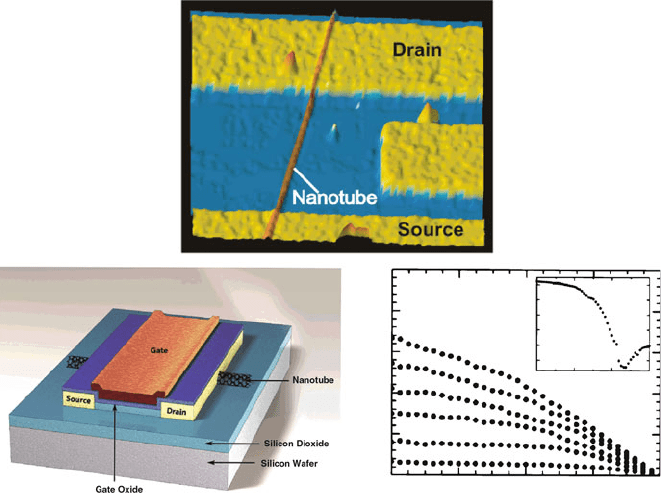
Another electronic application for CNTs is for next-generation field-effect
transistor (FET) designs. The “proof-of-concept” for CNTFETs was demonstrated
in the late 1990s, with a simple bridging of two noble metal electrodes with a
SWNT (Figure 6.67 – top). However, the electrical characteristics of this new
FET design were less than desirable, with high contact resistanc e (>1MO) and
low drive currents. Researchers at IBM have since modified the original design
wherein the semiconducting SWNTs are placed directly onto an oxidized Si
wafer, followed by the deposit ion of the source and drain (Co or Ti) electrodes
(Figure 6.67 – bottom). Through subsequent annealing, a stronger interaction is
afforded between the electrodes and CNT channel, which reduces the contact
resistance.
Though CNTFETs are in a relatively early stage of development, Avouris at IBM
provided a recent comparison of the output from a top-gate CNTFET (Figure 6.67 –
bottom) and existing Si-based FETs.
[182]
For CNTs with an average diameter of
1.4 nm, the ON current for a top-gated CNTFET is on the order of 2,100 mAmm
1
at
V
DS
(drain voltage) ¼ V
GS
(gate voltage)–V
T
(threshold voltage) ¼ 1.3 V. In com-
parison, the highest drive current in a p-CMOS under the same conditions is 650
mAmm
1
for a gate length of 50 nm. The transconductance (ratio of the output
current variation to the input voltage variation) of the CNTFET is 2,300 mSmm
1
;
the value for an analogous Si p-CMOS is 650 mSmm
1
. Hence, the values obtained
thus far show that CNTFETs outperform Si-based FETs. As improvements continue
to be made to the design of nanotube-based transistors, this technology should be
ready for the market just as the “glass ceiling” of Si CMOS devices is reached. It
should be noted that the extremely efficient thermal conductivity of CNTs will also
be exploited for cooling applications for future computers – of increasing concern as
the chip density continues to soar.
In addition to the above tunable conductive properties, CNTs are the strongest and
stiffest materials known to date (Table 6.6). The hollow, closed morphology of
536 6 Nanomaterials
nanotubes results in rather intriguing deformation modes in response to a mechanical
stress (Figure 6.68). In particular, it has been suggested that Stone–Wales defects may
become mobile under stress, which results in a change in tube diameter/chirality.
[183]
This also causes a change in the electronic properties of the CNT, opening up
possibilities for sensor applications. However, for MWNTs, studies have shown that
only the outer graphitic shell is able to support stress,
[184]
and SWNT bundles/ropes
(Figure 6.69) exhibit smaller Young’s moduli, relative to isolated SWNTs, due to weak
intertube cohesion.
[185]
Hence, although an individual SWNT has an elastic modulus of
1.2 TPa, the value for bundles is ca. 100 GPa for diameters in the range of 15–20 nm.
To improve the load distribution throughout the CNT and improve its mechanical
strength, there are efforts to create crosslinks between individual shells of MWNTs,
and among SWNTs within ropes.
The desirable mechanical properties of CNTs have been exploited in recent years
for the structu ral reinforcement of polymers.
[186]
This is a natural extension of
−1.6 −0.8 0.0 0.8
−1.1 V
−0.9 V
−0.7 V
−0.5 V
−0.3 V
−0.1 V
−1.6 −1.2 −0.8 −0.4 0.0
−5.0
−4.0
−3.0
−2.0
−1.0
0.0
Id [μA]
I
d
[A]
V
ds
[V]
V
gs
− V
t
−10
−6
−10
−7
−10
−8
−10
−9
−10
−10
−10
−11
V
gs
[V]
V
gs
= −0.6 V
Figure 6.67. Atomic force microscope (AFM) topographical image of an original CNTFET (top). The
source/drain electrodes were fabricated on a SiO
2
thin film grown on a Si wafer. The wafer itself served as
the gate electrode. Also shown (bottom) is an illustration of a top-gated CNTFET design, with an oxide
thickness of 15 nm and CNT length of 300 nm. The device electrical characteristics at room temperature is
also provided. The inset shows the transfer characteristic of the FET (output voltage of the device as a
function of the input voltage). Reproduced with permission from Avouris, P. Acc. Chem. Res. 2002, 35,
1026. Copyright 2002 American Chemical Society.
6.3. Nanoscale Building Blocks and Applications 537