Egerton R.F. Physical Principles of Electron Microscopy. An Introduction to TEM, SEM, and AEM
Подождите немного. Документ загружается.

142 Chapter 5
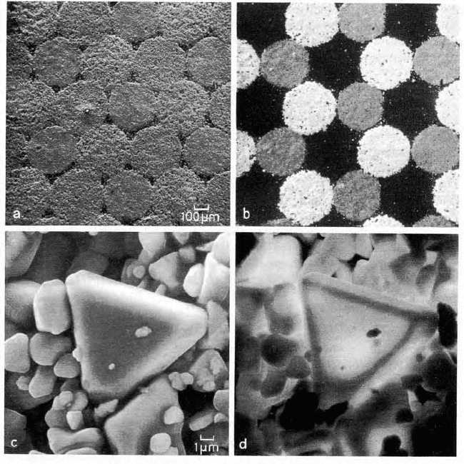
Figure 5-14. Red, green and blue phosphor dots in a color-TV screen, imaged using
secondary electrons (on the left) and in CL mode (on the right) without wavelength filtering.
The lower images show the individual grains of light-emitting phosphor imaged at higher
magnification. From Reimer (1998), courtesy of J. Hersener, Th. Ricker, and Springer-Verlag.
The light can be detected by a photomultiplier tube, sometimes preceded by
a color filter or a wavelength-dispersive device (glass prism or diffraction
grating) so that a limited range of photon wavelengths are recorded.
Cathodoluminescence is more efficient at low temperatures, so the specimen
s often cooled to below 20 K, using liquid helium as the refrigerant. i
Visible light is emitted when a primary electron, undergoing an inelastic
collision, transfers a few eV of energy to an outer-shell (valence) electron,
which then emits a photon while returning to its lowest-energy state. If the
primary electron collides with an inner-shell electron, more energy must be
transferred to excite the atomic electron to a vacant energy level (an outer
orbit or orbital) and a photon of higher energy (hundreds or thousands of eV)
The Scanning Electron Microscope 143
may be emitted as a characteristic x-ray photon. The x-ray energy can be
measured and used to identify the atomic number of the participating atom,
as discussed in Chapter 6. If the characteristic x-ray signal is used to control
the scanned-image intensity, the result is an elemental map showing the
distribution of a particular chemical element within the SEM specimen.
5.6 SEM Operating Conditions
The SEM operator is able to control several parameters of the SEM, such as
the electron-accelerating voltage, the distance of the specimen below the
objective lens, known as the working distance (WD), and sometimes the
diameter of the aperture used in the objective lens to control spherical
aberration. The choice of these variables in turn influences the performance
btained from the SEM.o
The accelerating voltage determines the kinetic energy E
0
of the primary
electrons, their penetration depth, and therefore the information depth of the
BSE image. As we have seen, secondary electrons are generated within a
very shallow escape depth below the specimen surface, therefore the SE
image might be expected to be independent of the choice of E
0
. However,
only part of the SE signal (the so-called SE1 component) comes from the
generation of secondaries by primary electrons close to the surface. Other
components (named SE2 and SE3, respectively) arise from the secondaries
generated by backscattered electrons, as they exit the specimen, and from
backscattered electrons that strike an internal surface of the specimen
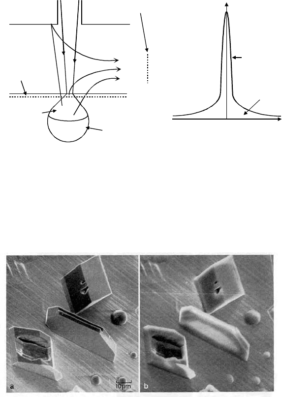
chamber; see Fig. 5-15a. As a result of these SE2 and SE3 components,
secondary-electron images can show contrast from structure present well
below the surface (but within the primary-electron penetration depth), and
this structure results from changes in backscattering coefficient, for example
due to local differences in atomic number. Such effects are more prominent
if the primary-electron penetration depth is large, in other words at a higher
accelerating voltage, making the sample appear more “transparent” in the SE
image; see Fig. 5-16. Conversely, if the accelerating voltage is reduced
below 1 kV, the penetration depth becomes very small (even compared to
the secondary-electron escape depth) and only surface features are seen in
the SE and BSE images.
Because the primary beam spreads laterally as it penetrates the specimen
and because backscattering occurs over a broad angular range, some SE2
electrons are generated relatively far from the entrance of the incident probe
and reflect the properties of a large part of the primary-electron interaction
volume. The SE3 component also depends on the amount of backscattering
from this relatively large volume. In consequence, the spatial resolution of
144 Chapter 5
the SE2 and SE3 components is substantially worse than for the SE1
component; the SE2 and SE3 electrons contribute a tail or skirt to the image-
resolution function; see Fig. 5-15b. Although this fact complicates the
definition of spatial resolution, the existence of a sharp central peak in the
resolution function ensures that some high-resolution information will be
present in a secondary-electron image.
SE1
SE2
SE3
objective
escape depth
BSE escape
volume
interaction
volume
grid of SE
detector
0
number of
secondaries
distance from center of probe
SE1 peak
SE2 + SE3
(a) (b)
Figure 5-15. (a) Generation of SE1 and SE2 electrons in a specimen, by primary electrons and
by backscattered electrons, respectively. SE3 electrons are generated outside the specimen
when a BSE strikes an internal SEM component, in this case the bottom of the objective lens.
(b) Secondary-image resolution function, showing the relative contributions from secondaries
generated at different distances from the center of the electron probe.
Figure 5-16. SE images of tridymite crystals and halite spheres on a gold surface, recorded
with an SEM accelerating voltage of (a) 10 kV and (b) 30 kV. Note the higher transparency at
higher incident energy. From Reimer (1998), courtesy of R. Blaschke and Springer-Verlag.
The Scanning Electron Microscope 145
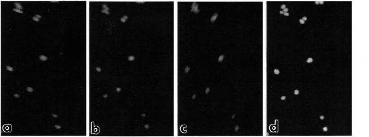
Figure 5-17. (a – c) Astigmatic SE image showing the appearance of small particles as the
objective current is changed slightly; in (b) the focus is correct, but the resolution is less than
optimum. (d) Correctly focused image after astigmatism correction.
Because the incident beam spreads out very little within the SE1 escape
depth, the width of this central peak (Fig. 5-15b) is approximately equal to
the diameter d of the electron probe, which depends on the electron optics of
the SEM column. To achieve high demagnification of the electron source,
the objective lens is strongly excited, with a focal length below 2 cm. This in
turn implies small C
s
and C
c
(see Chapter 2), which reduces broadening of
the probe by spherical and chromatic aberration. Because of the high
demagnification, the image distance of the objective is approximately equal
to its focal length (see Section 3.5); in other words, the working distance
needs to be small to achieve the best SEM resolution. The smallest available
values of d (below 1 nm) are achieved by employing a field-emission source,
which provides an effective source diameter of only 10 nm (see Table 3-1),
and a working distance of only a few millimeters.
Of course, good image resolution is obtained only if the SEM is properly
focused, which is done by carefully adjusting the objective-lens current.
Small particles on the specimen offer a convenient feature for focusing; the
objective lens current is adjusted until their image is as small and sharp as
possible. Astigmatism of the SEM lenses can be corrected at the same time;
the two stigmator controls are adjusted so that there is no streaking of image
features as the image goes through focus (see Fig. 5-17), similar to the
commonly-used TEM procedure. In the SEM, zero astigmatism corresponds
to a round (rather than elliptical) electron probe, equivalent to an axially-
symmetric resolution function.
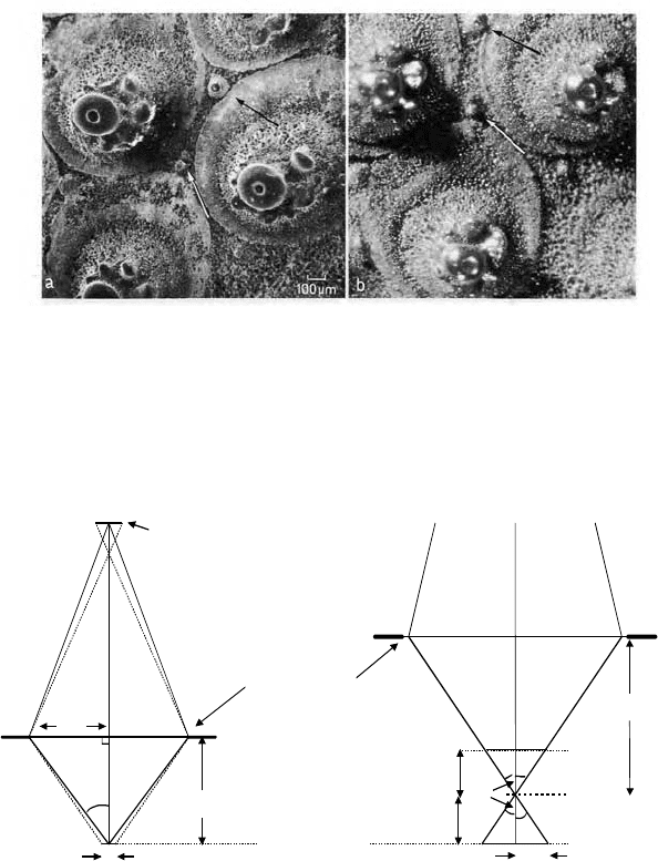
As shown in Fig. 5-18, the SEM not only has better resolution than a
light microscope but also a greater depth of field. The latter can be defined
as the change 'v in specimen height (or working distance) that produces a
146 Chapter 5
just-observable loss ('r) in image resolution. As seen from Fig. 5-19b, 'r |
D/'v where D is the convergence semi-angle of the probe. Taking 'r as
equal to the image resolution, so that the latter is degraded by a factor |2
by the incorrect focus (as discussed for the TEM in Section 3.7) and taking
this resolution as equal to the probe diameter (assuming SE imaging),
'v |'r / D|d / D (5.5)
Figure 5-18. (a) Low-magnification SEM image of a sea-urchin specimen, in which specimen
features at different height are all approximately in focus. (b) Light-microscope of the same
area, in which only one plane is in focus, other features (such as those indicated by arrows)
appearing blurred. From Reimer (1998), courtesy of Springer-Verlag.
D
D
v= WD
image of electron source
demagnified by the
condenser lens(es)
d
D/2
'
r
'
v
(a)
(b)
objective lens
v =WD
'
v
specimen
Figure 5-19. (a) The formation of a focused probe of diameter d by the SEM objective lens.
(b) Increase 'r in electron-probe radius for a plane located a distance 'v above or below the
plane of focus.
The Scanning Electron Microscope 147
The large SEM depth of field is seen to be a direct result of the relatively
small convergence angle D of the electron probe, which in turn is dictated by
the need to limit probe broadening due to spherical and chromatic aberration.
As shown in Fig. 5-19a,
D|D/(2v) (5.6)
According to Eqs. (5.5) and (5.6), the depth of field 'v can be increased by
increasing v or reducing D , although in either case there may be some loss
of resolution because of increased diffraction effects (see page 4). Most
SEMs allow the working distance to be changed, by height adjustment of the
specimen relative to the lens column. Some microscopes also provide a
choice of objective diaphragm, with apertures of more than one diameter.
Because of the large depth of field, the SEM specimen can be tilted
away from the horizontal and toward the SE detector (to increase SE yield)
without too much loss of resolution away from the center of the image. Even
so, this effect can be reduced to zero (in principle) by a technique called
dynamic focusing. It involves applying the x- and/or y-scan signal (with an
appropriate amplitude, which depends on the angle of tilt) to the objective-
current power supply, in order to ensure that the specimen surface remains in
focus at all times during the scan. This procedure can be regarded as an
adaptation of Maxwell’s third rule of focusing (see Chapter 2) to deal with a
non-perpendicular image plane. No similar option is available in the TEM,
where the post-specimen lenses image all object points simultaneously.
5.7 SEM Specimen Preparation
One major advantage of the SEM (in comparison to a TEM) is the ease of
specimen preparation, a result of the fact that the specimen does not have to
be made thin. In fact, many conducting specimens require no special
preparation before examination in the SEM. On the other hand, specimens of
insulating materials do not provide a path to ground for the specimen current
I
s
and may undergo electrostatic charging when exposed to the electron
probe. As is evident from Eq. (5.4), this current can be of either sign,
depending on the values of the backscattering coefficient K and secondary-
electron yield G. Therefore, the local charge on the specimen can be positive
or negative. Negative charge presents a more serious problem, as it repels
the incident electrons and deflects the scanning probe, resulting in image
distortion or fluctuations in image intensity.
One solution to the charging problem is to coat the surface of the SEM
specimen with a thin film of metal or conducting carbon. This is done in
vacuum, using the evaporation or sublimation technique already discussed in
148 Chapter 5
Section 4-10. Films of thickness 10 20 nm conduct sufficiently to prevent
charging of most specimens. Because this thickness is greater than the SE
escape depth, the SE signal comes from the coating rather than from the
specimen material. However, the external contours of a very thin film
closely follow those of the specimen, providing the possibility of a faithful
topographical image. Gold and chromium are common coating materials.
Evaporated carbon is also used; it has a low SE yield but an extremely small
grain size so that granularity of the coating does not appear (as an artifact) in
a high-magnification SE image, masking real specimen features.
Where coating is undesirable or difficult (for example, a specimen with
very rough surfaces), specimen charging can often be avoided by carefully
choosing the SEM accelerating voltage. This option arises because the
backscattering coefficient K and secondary-electron yield G depend on the
primary-electron energy E
0
. At high E
0
, the penetration depth is large and
only a small fraction of the secondary electrons generated in the specimen
can escape into the vacuum. In addition, many of the backscattered electrons
are generated deep within the specimen and do not have enough energy to
escape, so K will be low. A low total yield (K + G) means that the specimen
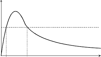
charges negatively; according to Eq. (5.4). As E
0
is reduced, G increases and
the specimen current I
s
required to maintain charge neutrality eventually falls
to zero at some incident energy E
2
corresponding to (K + G) = 1. Further
reduction in E
0
could result in a positive charge but this would attract
secondaries back to the specimen, neutralizing the charge. So in practice,
positive charging is less of a problem.
For an incident energy below some value E
1
, the total yield falls below
one because now the primary electrons do not have enough energy to create
secondaries. Because by definition K < 1, Eq. (5.4) indicates that negative
charging will again occur. But for E
1
< E
0
< E
2
, negative charging is absent
even for an insulating specimen, as shown in Fig. 5-20.
E
0
E
1
E
2
1
total yield (
KG
)
zero-
charging
region
Figure 5-20. Total electron yield (K + G) as a function of primary energy, showing the range
(E
1
to E
2
) over which electrostatic charging of an insulating specimen is not a problem.
The Scanning Electron Microscope 149
Typically, E
2
is in the range 1 10 keV. Although there are tables giving
values for common materials (Joy and Joy, 1996), E
2
is usually found
experimentally, by reducing the accelerating voltage until charging artifacts
(distortion or pulsating of the image) disappear. E
1
is typically a few hundred
volts, below the normal range of SEM operation.
The use of low-voltage SEM is therefore a practical option for imaging
insulating specimens. The main disadvantage of low E
0
is the increased
chromatic-aberration broadening of the electron probe, given approximately
by r
c
= C
c
D('E/E
0
). This problem can be minimized by using a field-
emission source (which has a low energy spread: 'E < 0.5 eV) and by
careful design of the objective lens to reduce the chromatic-aberration
coefficient C
c
. This is an area of continuing research and development.
5.8 The Environmental SEM
An alternative approach to overcoming the specimen-charging problem is to
surround the specimen with a gaseous ambient rather than high vacuum. In
this situation, the primary electrons ionize gas molecules before reaching the
specimen. If the specimen charges negatively, positive ions are attracted
toward it, largely neutralizing the surface charge.
Of course, there must still be a good vacuum within the SEM column in
order to allow the operation of a thermionic or field-emission source, to
enable a high voltage to be used to accelerate the electrons and to permit the
focusing of electrons without scattering from gas molecules. In an
environmental SEM (also called a low-vacuum SEM), primary electrons
encounter gas molecules only during the last few mm of their journey, after
being focused by the objective lens. A small-diameter aperture in the bore of
the objective allows the electrons to pass through but prevents most gas
molecules from traveling up the SEM column. Those that do so are removed
by continuous pumping. In some designs, a second pressure-differential
aperture is placed just below the electron gun, to allow an adequate vacuum
to be maintained in the gun, which has its own vacuum pump.
The pressure in the sample chamber can be as high as 5000 Pa (0.05
atmosphere), although a few hundred Pascal is more typical. The gas
surrounding the specimen is often water vapor, as this choice allows wet
specimens to be examined in the SEM without dehydration, provided the
specimen-chamber pressure exceeds the saturated vapor pressure (SVP) of
water at the temperature of the specimen. At 25qC, the SVP of water is about
3000 Pa. However the required pressure can be reduced by a factor of 5 or
more by cooling the specimen, using a thermoelectric element incorporated
into the specimen stage.
150 Chapter 5
A backscattered-electron image can be obtained in the environmental
SEM, using the detectors described previously. An Everhart-Thornley
detector cannot be used because the voltage used to accelerate secondary
electrons would cause electrical discharge within the specimen chamber.
Instead, a potential of a few hundred volts is applied to a ring-shaped
electrode just below the objective lens; secondary electrons initiate a
controlled discharge between this electrode and the specimen, resulting in a
current that is amplified and used as the SE signal.
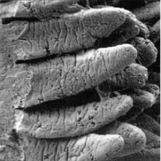
Examples of specimens that have been successfully imaged in the
environmental SEM include plant and animal tissue (see Fig. 5-21), textile
specimens (which charge easily in a regular SEM), rubber, and ceramics.
Oily specimens can also be examined without contaminating the entire SEM;
hydrocarbon molecules that escape through the differential aperture are
quickly removed by the vacuum pumps.
The environmental chamber extends the range of materials that can be
examined by SEM and avoids the need for coating the specimen to make it
conducting. The main drawback to ionizing gas molecules during the final
phase of their journey is that the primary electrons are scattered and
deflected from their original path. This effect adds an additional skirt (tail) to
the current-density distribution of the electron probe, degrading the image
resolution and contrast. Therefore, an environmental SEM would usually be
operated as a high-vacuum SEM (by turning off the gas supply) in the case
of conductive specimens that no not have a high vapor pressure.
Figure 5-21. The inner wall of the intenstine of a mouse, imaged in an environmental SEM.
The width of the image is 0.7 mm. Courtesy of ISI / Akashi Beam Technology Corporation.
The Scanning Electron Microscope 151
5.9 Electron-Beam Lithography
Electrons can have a permanent effect on an electron-microscope specimen,
generally known as radiation damage. In inorganic materials, high-energy
electrons that are “elastically” scattered through large angles can transfer
enough energy to atomic nuclei to displace the atoms from their lattice site in
a crystal, creating displacement damage visible in a TEM image, such as the
point-defect clusters shown in Fig. 4-16. In organic materials, radiation
damage occurs predominantly as a result of inelastic scattering; the bonding
configuration of valence electrons is disturbed, often resulting in the
permanent breakage of chemical bonds and the destruction of the original
structure of the solid. This makes it difficult to perform high-resolution
microscopy (TEM or SEM) on organic materials, such as polymers (plastics)
nd impossible to observe living tissue at a subcellular level. a
However, radiation damage is put to good use in polymer materials
known as resists, whose purpose is to generate structures that are
subsequently transferred to a material of interest, in a process referred to as
lithography. In a positive resist, the main radiation effect is bond breakage.
As a result, the molecular weight of the polymer decreases and the material
becomes more soluble in an organic solvent. If an SEM is modified slightly
by connecting its x and y deflection coils to a pattern generator, the electron
beam is scanned in a non-raster manner and a pattern of radiation damage is
produced in the polymer. If the polymer is a thin layer on the surface of a
substrate, such as a silicon wafer, subsequent “development” in an organic
solvent results in the scanned pattern appearing as a pattern of bare substrate.
The undissolved areas of polymer form a barrier to chemical or ion-beam
etching of the substrate (Section 4.10), hence it acts as a “resist.” After
etching and removing the remaining resist, the pattern has been transferred
to the substrate and can be used to make useful devices, often in large
number. The fabrication of silicon integrated circuits (such as computer
chips) makes use of this process, repeated many times to form complex
multilayer structures, but using ultraviolet light or x-rays as the radiation
source. Electrons are used for smaller-scale projects, requiring high
resolution but where production speed (throughput) is less important. Resist
exposure is done using either a specialized electron-beam writer or an SEM.
In a negative resist, radiation causes an increase in the extent of chemical
bonding (by “cross-linking” organic molecules), giving an increase in
molecular weight and a reduction in solubility in exposed areas. After
development, the pattern is a “negative” of the beam-writing pattern, in the
sense that resist material remains in areas where the beam was present
(similar to undissolved silver in a black-and-white photographic negative).
