Egerton R.F. Physical Principles of Electron Microscopy. An Introduction to TEM, SEM, and AEM
Подождите немного. Документ загружается.

132 Chapter 5
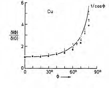
Figure 5-5. Dependence of SE yield on the angle of tilt M of the specimen, measured between
a plane perpendicular to its surface and the primary-electron beam (M = 0 corresponds to
normal incidence). Data points represent experimental measurements and Monte Carlo
predictions for copper; the curve represents a 1/cos M function. From Reimer (1998), courtesy
of Springer-Verlag.
(close to the surface) and on the primary-electron energy E
0.
. For a given
specimen, G decreases with increasing E
0
because higher-energy primaries
undergo less inelastic scattering (per unit distance traveled) and so there will
be fewer secondaries generated within the escape depth.
As Fig. 5-5 indicates, the secondary-electron yield also depends on the
angle between the incoming primary electron and the surface. The yield is
lowest for normal (perpendicular) incidence and increases with increasing
angle between the primary beam and the surface-normal. The reason is
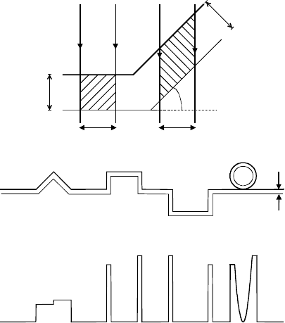
illustrated in Fig. 5-6a, which shows a focused nearly-parallel beam of
primary electrons (diameter d ) incident at two locations on a specimen,
where the surface is normal (at A) and inclined (at B) to the incident beam.
The region from which secondary electrons can escape is such that all points
within it lie within the escape depth O of the surface. For normal incidence,
this escape region is a cylinder of radius d/2, height O
, and volume V(0) =
(S/4) d
2
O . For the inclined surface, the escape region is a slanted cylinder
with height O (perpendicular to the surface) and base of cross-sectional area
(S/4)(d /cos I)
2
, giving escape volume V(I) = S(d/2)
2
(O/cosI) = V(0)/cosI.
Because the SE yield is proportional to the number of SE generated within
the escape region, G is proportional to the escape volume, resulting in:
G(I) = G(0)/cosI (5.3)
Measurements of G(I) support this inverse-cosine formula; see Fig. 5-5.
The Scanning Electron Microscope 133
(a)
(b)
(c)
O
O
O
A
B
d
d
I
Figure 5-6. (a) SEM incident beam that is normal to a specimen surface (at A) and inclined to
the surface (at B). The volume from which secondaries can escape is proportional to the
shaded cross-sectional area, which is Od for case A and Od/cos I for a tilted surface (case B).
(b) Cross-sectional diagram of a specimen surface that contains triangular and square
protrusions, a square-shaped trough or well, and a spherical particle; O is the SE escape depth.
(c) Corresponding secondary-electron signal (from a line-scan along the surface), assuming a
SE detector that is located to the right of the specimen.
In qualitative terms, non-normal irradiation of a surface generates more
SE that lie within a perpendicular distance O of the surface and can therefore
escape into the vacuum. For a surface with topographical (height) variations
(Fig. 5-6b), this orientation dependence of G results in protruding or recessed
features appearing bright in outline in the SE image (Figs. 5-6c and 5-7a),
sim lar to thickness-gradient contrast from a TEM replica.i
In practice, there is usually some asymmetry due to the fact that the SE
detector is located to one side of the column (Fig. 5-1) rather than directly
above. Surface features that are tilted toward the detector appear especially
bright because electrons emitted from these regions have a greater
probability of reaching the detector; see Fig. 5-7a. This fact can be used to
distinguish raised features and depressions in the surface of the specimen, as
illustrated in Fig. 5-6c. As a result, the SE image has a three-dimensional
appearance, similar to that of a rough surface obliquely illuminated by light,
which makes the topographical contrast relatively easy to interpret; see also
Fig. 5-9a.
134 Chapter 5
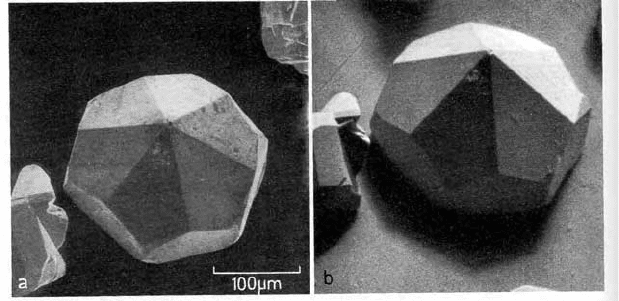
Figure 5-7. (a) Secondary-electron image of a small crystal; the side-mounted Everhart-
Thornley detector is located toward the top of the image. (b) Backscattered-electron image
recorded by the same side-mounted detector, which also shows topographical contrast and
shadowing effects. Such contrast is much weaker for a BSE detector mounted directly above
the specimen. From Reimer (1998), courtesy of Springer-Verlag.
Taking advantage of the orientation dependence of G, the whole sample is
often tilted away from a horizontal plane and toward the detector, as shown
in Fig. 5-1. This increases the overall SE signal, averaged over all regions of
the sample, while preserving the topographic contrast due to differences in
surface orientation.
To further increase the SE signal, a positively-biased electrode is used to
attract the secondary electrons away from the specimen. This electrode could
be a simple metal plate that absorbs the electrons, generating a small current
that could be amplified and used to generate a SE image. However, the
resulting SE signal would be weak and noisy. The amount of electronic noise
could be reduced by limiting the frequency response (bandwidth) of the
amplifier, but the amplified signal might not follow the fast changes in input
signal that occur when the electron probe is scanned rapidly over a non-
uniform specimen.
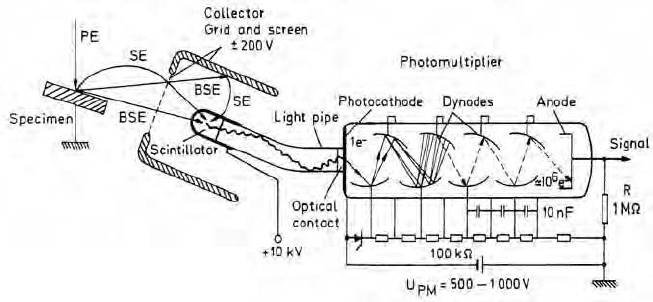
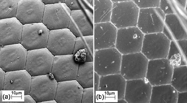
A stronger signal is obtained from an Everhart-Thornley detector, named
after the scientists who first applied this design to the SEM. The secondaries
are first attracted toward a wire-mesh electrode biased positively by a few
hundred volts; see Fig. 5-8. Most of the electrons pass through the grid and
are accelerated further toward a scintillator that is biased positive V
s
by
several thousand volts. The scintillator can be a layer of phosphor (similar to
the coating on a TEM screen) on the end of a glass rod, or a light-emitting
plastic or a garnet (oxide) material, each made conducting by a thin metallic
surface coating. The scintillator has the property (cathodoluminescence) of
The Scanning Electron Microscope 135
emitting visible-light photons when bombarded by charged particles such as
electrons. The number of photons generated by each electron depends on its
kinetic energy E
k
(= eV
s
) and is of the order 100 for V
s
| 10 kV. The
scintillator material has a high refractive index, so advantage can be taken of
total internal reflection to guide the photons through a light pipe (a solid
plastic or glass rod passing through a sealed port in the specimen chamber)
to a photomultiplier tube (PMT) located outside the vacuum.
The PMT is a highly sensitive detector of visible (or ultraviolet) photons
and consists of a sealed glass tube containing a hard (good-quality) vacuum.
The light-entrance surface is coated internally with a thin layer of a material
with low work function, which acts as a photocathode. When photons are
absorbed within the photocathode, they supply sufficient energy to liberate
conduction or valence electrons, which may escape into the PMT vacuum as
photoelectrons. These low-energy electrons are accelerated toward the first
of a series of dynode electrodes, each biased positive with respect to the
photocathode.
At the first dynode, biased at 100 200 V, the accelerated photoelectrons
generate secondary electrons within the escape depth, just like primary
electrons striking an SEM specimen. The dynodes are coated with a material
with high SE yield (G) so that at least two (sometimes as many as ten)
secondary electrons are emitted for each photoelectron. The secondaries are
accelerated toward a second dynode, biased at least 100 V positive with
respect to the first, where each secondary produces at least two new
secondaries. This process is repeated at each of the n (typically eight)
dynodes, resulting in a current amplification factor of (G)
n
, typically | 10
6
for
n = 8 and G|4.
Figure 5-8. A typical scintillator/PMT (Everhart-Thornley) detector, employed for secondary-
electron imaging in the SEM. From Reimer (1998), courtesy of Springer-Verlag.
136 Chapter 5
Because each secondary produced at the SEM specimen generated about
100 photoelectrons, the overall amplification (gain) of the PMT/scintillator
combination can be as high as 10
8
, depending on how much accelerating
voltage is applied to the dynodes. Although this conversion of SEM
secondaries into photons, then into photoelectrons and finally back into
secondary electrons seems complicated, it is justified by the fact that the
detector provides high amplification with relatively little added noise.
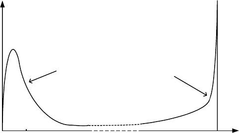
In some high-resolution SEMs, the objective lens has a small focal length
(a few millimeters) and the specimen is placed very close to it, within the
magnetic field of the lens (immersion-lens configuration). Secondary
electrons emitted close to the optic axis follow helical trajectories, spiraling
around the magnetic-field lines and emerging above the objective lens,
where they are attracted toward a positively-biased detector. Because the
signal from such an in-lens detector (or through-the-lens detector)
corresponds to secondaries emitted almost perpendicular to the specimen
surface, positive and negative values of I (Fig. 5-6a) provide equal signal.
Consequently, the SE image shows no directional or shadowing effects, as
illustrated in Fig. 5-9b.
In-lens detection is often combined with energy filtering of the secondary
electrons that form the image. For example, a Wien-filter arrangement
(Section 7.3) can be used to select higher-energy secondaries, which consist
mainly of the higher-resolution SE1 component (Section 5.6).
Figure 5-9. Compound eye of an insect, coated with gold to make the specimen conducting.
(a) SE image recorded by a side-mounted detector (located toward the top of the page) and
showing a strong directional effect, including dark shadows visible below each dust particle.
(b) SE image recorded by an in-lens detector, showing topographical contrast but very little
directional or shadowing effect. Courtesy of Peng Li, University of Alberta.
The Scanning Electron Microscope 137
5.4 Backscattered-Electron Images
A backscattered electron (BSE) is a primary electron that has been ejected
from a solid by scattering through an angle greater than 90 degrees. Such
deflection could occur as a result of several collisions, some or all of which
might involve a scattering angle of less than 90 degrees; however, a single
elastic event with T > 90 degrees is quite probable. Because the elastic
scattering involves only a small energy exchange, most BSEs escape from
the sample with energies not too far below the primary-beam energy; see
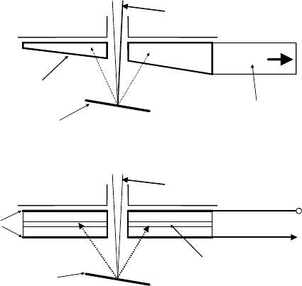
Fig. 5-10. The secondary and backscattered electrons can therefore be
distinguished on the basis of their kinetic energy.
Because the cross section for high-angle elastic scattering is proportional
to Z
2
, we might expect to obtain strong atomic-number contrast by using
backscattered electrons as the signal used to modulate the SEM-image
intensity. In practice, the backscattering coefficient K (the fraction of
primary electrons that escape as BSE) does increase with atomic number,
(almost linearly for low Z), and BSE images can show contrast due to
variations in chemical composition of a specimen, whereas SE images reflect
mainly its surface topography.
Another difference between the two kinds of image is the depth from
which the information originates. In the case of a BSE image, the signal
comes from a depth of up to about half the penetration depth (after being
generated, each BSE must have enough energy to get out of the solid). For
primary energies above 3 kV, this means some tens or hundreds of
nanometers rather than the much smaller SE escape depth ( | 1 nm).
E
0
kinetic energy of emitted electrons
10 eV
number of electrons
per eV of KE
S E
B S E
0
Figure 5-10. Number of electrons emitted from the SEM specimen as a function of their
kinetic energy, illustrating the conventional classification into secondary and backscattered
components.
138 Chapter 5
Backscattered electrons can be detected by a scintillator/PMT detector if
the bias on the first grid is made negative, to repel secondary electrons. The
BSEs are recorded if they impinge directly on the scintillator (causing light
emission) or if they strike a surface beyond the grid and create secondaries
that are then accelerated to the scintillator (see Fig. 5-8). The BSEs travel in
almost a straight line, their high energy making them relatively unresponsive
to electrostatic fields. Consequently, more of them reach the side-mounted
detector if they are emitted from a surface inclined toward it, giving some
topographical contrast; as in Fig. 5-7b. However, backscattered electrons are
emitted over a broad angular range, and only those emitted within a small
solid angle (defined by the collector diameter) reach the scintillator. The
resulting signal is weak and provides a noisy image, so a more efficient form
of detector is desirable.
In the so-called Robinson detector, an annular (ring-shaped) scintillator
is mounted immediately below the objective lens and just above the
specimen; see Fig. 5-11a. The scintillator subtends a large solid angle and
collects a substantial fraction of the backscattered electrons. Light is
channeled (by internal reflection) through a light pipe and into a PMT, as in
the case of the Everhart-Thornley detector.
An alternative backscattered-electron detector is shown in Fig. 5-11b.
This solid-state detector consists of a large area (several cm
2
) silicon diode,
scintillator
light pipe
specimen
specimen
p-n transition region
metal
contacts
signal
HV
objective
objective
primary beam
primary beam
(a)
(b)
light
to PMT
Figure 5-11. Backscattered-electron detectors installed below the objective lens of an SEM:
(a) annular-scintillator/PMT (Robinson) design and (b) solid-state (semiconductor) detector.
The Scanning Electron Microscope 139
mounted just below the objective lens. Impurity atoms (arsenic, phosphorus)
are added to the silicon to make it electrically conducting. The diode consists
of an n-type layer, in which conduction is by electrons, and a p-type layer, in
which conduction is by holes (absence of electrons in an otherwise full
valence band). At the interface between the p- and n-layers lies a transition
region, in which current carriers (electrons and holes) are absent because
they have diffused across the interface. A voltage applied between the n- and
p-regions (via metal surface electrodes) will therefore create a high internal
electric field across this high-resistivity transition region. If a backscattered
electron arrives at the detector and penetrates to the transition region, its
remaining kinetic energy is used to excite electrons from the valence to the
conduction band, creating mobile electrons and holes. These free carriers
move under the influence of the internal field, causing a current pulse to
flow between the electrodes and in an external circuit. BSE arrival can
therefore be measured by counting current pulses or by measuring the
average current, which is proportional to the number of backscattered
electrons arriving per second. Because secondary electrons do not have
enough energy to reach the transition region, they do not contribute to the
signal provided by the solid-state detector.
Because the Robinson and solid-state detectors are mounted directly
above the specimen, their BSE signal contains little topographic contrast but
does show “material contrast” due to differences in local atomic number in
the near-surface region of the specimen. The orientation of crystal planes
(relative to the incident beam) also affects the electron penetration into the
specimen, through diffraction effects, which gives rise to some “orientation
contrast” between the different grains in a polycrystalline specimen.
5.5 Other SEM Imaging Modes
Although SE and BSE images suffice for most SEM applications, some
specimens benefit from the ability to use other types of signal to modulate
the image intensity, as we now illustrate with several examples.
A specimen-current image is obtained by using a specimen holder that
is insulated from ground and connected to the input terminal of a sensitive
current amplifier. Conservation of charge implies that the specimen current
I
s
flowing to ground (through the amplifier) must be equal to the primary-
beam current I
p
minus the rate of loss of electrons from secondary emission
and backscattering:
I
s
= I
p
I
BSE
I
SE
= I
p
(1 KG) (5.4)
140 Chapter 5
Whereas I
p
remains constant, I
BSE
and I
SE
vary, due to variations in K and G,
as the probe scans across the specimen. Therefore the specimen-current
image contains a mixture of Z-contrast and topographical information. To
reduce the noise level of the image, the current amplifier must be limited in
bandwidth (frequency range), requiring that the specimen be scanned slowly,
ith a frame time of many seconds.w
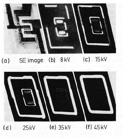
Electron-beam induced conductivity (EBIC) occurs when the primary-
electron probe passes near a p-n junction in a semiconductor specimen such
as a silicon integrated circuit (IC) containing diodes and transistors.
Additional electrons and holes are created, as in the case of a solid-state
detector responding to backscattered electrons, resulting in current flow
between two electrodes attached to the specimen surface. If this current is
used as the signal applied to the image display, the junction regions show up
bright in the EBIC image. The p-n junctions in ICs are buried below the
surface, but provided they lie within the penetration depth of the primary
electrons, an EBIC signal will be generated. It is even possible to use the
dependence of penetration depth on primary energy E
0
to image junctions at
different depths; see Fig. 5-12.
Figure 5-12. Imaging of perpendicular p-n junctions in a MOS field-effect transistor
(MOSFET). (a) SE image, (b – f) EBIC images for increasing primary-electron energy
E
0
and
therefore increasing penetration depth. Reproduced from Reimer (1998), courtesy of H. Raith
and Springer-Verlag.
The Scanning Electron Microscope 141
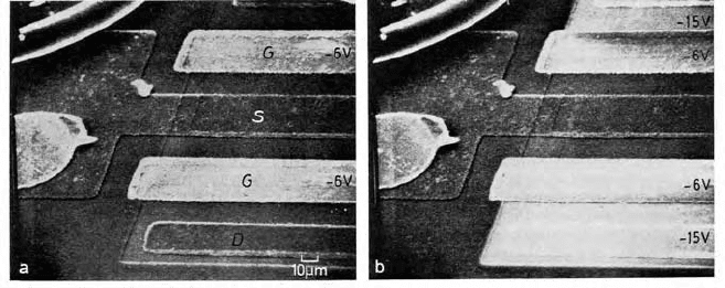
Figure 5-13. SEM voltage-contrast image of an MOS field-effect transistor with (a) the gate
electrode G at –6 V, source S and drain D electrodes grounded; (b) gate at –6 V, source and
drain at –15 V. From Reimer (1998), courtesy of Springer-Verlag.
Voltage contrast arises when voltages are applied to surface regions of a
specimen, usually a semiconductor IC chip. The secondary-electron yield is
reduced in regions that are biased positive, as lower-energy secondaries are
attracted back to the specimen. Conversely, negative regions exhibit a higher
SE yield (see Fig. 5-13) because secondaries are repelled and have a higher
probability of reaching the detector. The voltage-contrast image is useful for
checking whether supply voltages applied to an integrated circuit are
reaching the appropriate locations. It can also be used to test whether a
circuit is operating correctly, with signal voltages appearing in the right
sequence. Although most ICs (such as microprocessors) operate at far too
high a frequency for their voltage cycles to be observed directly, this
sequence can be slowed down and viewed in a TV-rate SEM image by use
of a stroboscopic technique. By applying a square-wave current to
deflection coils installed in the SEM column, the electron beam can be
periodically deflected and intercepted by a suitably-placed aperture. If this
chopping of the beam is performed at a frequency that is slightly different
from the operational frequency of the IC, the voltage cycle appears in the SE
image at the beat frequency (the difference between the chopping and IC
frequencies), which could be as low as one cycle per second.
As an alternative to collecting electrons to form an SEM image, it is
sometimes possible to detect photons emitted from the specimen. As
discussed in connection with a scintillator detector, some materials emit
visible light in response to bombardment by electrons, the process known as
cathodoluminescence (CL). In addition to phosphors (see Fig. 5-14), certain
semiconductors fall into this category and may emit light uniformly except in
regions containing crystal defects. In such specimens, CL images have been
used to reveal the presence of dislocations, which appear as dark lines.
