Chung Y.-W. Practical guide to surface science and spectroscopy
Подождите немного. Документ загружается.

147
8.3 WORK FUNCTION MEASUREMENTS
8.3.1 Photoemission
Consider a metal surface illuminated by monoenergetic photons of
energy h greater than the work function of the metal surface. One can
readily show that the work function is given by h ⫺ energy width of
the photoelectron spectrum, provided that E
VA C
for the sample is higher
than that for the spectrometer. This gives the absolute value of the
work function. The accuracy of this technique is determined by the
ability to locate the start of the secondary electron background and the
Fermi edge and is about 0.1 eV.
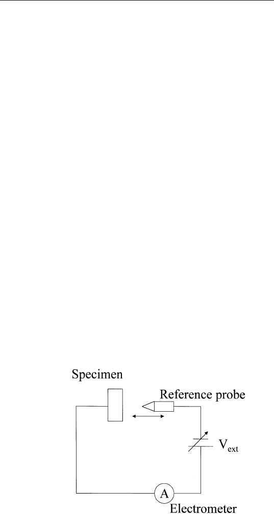
8.3.2 Kelvin Method
The Kelvin method is used to measure work function changes relative
to a reference probe surface that has a stable work function value, as
illustrated in Fig. 8.10. One places a reference probe close to the surface
of interest and sets it into vibration at a certain frequency. This forms
a capacitor of capacitance C. The work function difference ⌬V between
the sample and the reference surface appears as a difference in the
surface potential between the two surfaces. In the presence of an external
bias, the charge on the capacitor plate Q is therefore given by Q ⫽ C
(⌬V ⫹ V
ext
), where V
ext
is the external bias.
The vibration of the reference probe causes C to change with time,
resulting in an alternating current I (⫽dQ/dt) ⫽ (V ⫹ V
ext
) dC/dt. When
V
ext
⫽⫺⌬V, the net surface potential difference across the capacitor
FIGURE 8.10 The Kelvin vibrating probe method to measure work function
changes.

148
CHAPTER 8 / METAL–SEMICONDUCTOR INTERFACES
vanishes, and the current I goes to zero. This therefore gives the work
function relative to the reference probe surface. The accuracy is ⬃
1–10 meV.
8.3.3 Retarding Field Technique
This is applied in a retarding field analyzer apparatus. A beam of
monoenergetic electrons (preferably low energy) impinges on the speci-
men surface, and the current flowing into the specimen is measured
as a function of the retarding voltage applied to the specimen. The
current vanishes when the vacuum level of the specimen is just above
that of the filament. If the work function of the specimen changes, the
amount of retarding voltage required to reduce the specimen current
to zero will be changed. The difference in the retarding voltage is equal
to the work function change, assuming that the filament work function
is not altered in these measurements. The accuracy is ⬃ 10–100 meV.
8.4 THE METAL–SEMICONDUCTOR INTERFACE
8.4.1 The Schottky Model
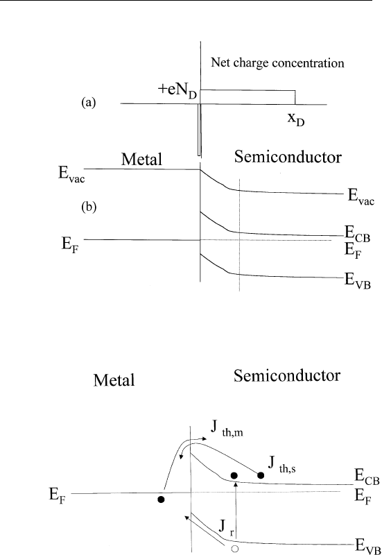
Consider a metal/n-type semiconductor interface, with the work func-
tion of the metal greater than that of the semiconductor. The Schottky
model assumes that there are no interface states. When
M
⬎
SC
,
electrons flow from the semiconductor to the metal when the contact
is made, resulting in the formation of a depletion region in the semicon-
ductor. The resulting charge distribution is shown in Fig. 8.11a and
the corresponding electron energy band diagram in Fig. 8.11b. In this
configuration, electrons flow from the metal to the semiconductor via
thermal excitation (J
th,m
) over the Schottky barrier (E
CB
⫺ E
F
). Elec-
trons also flow from the semiconductor to the metal (J
th,s
) by climbing
over the depletion region barrier V
BB
. Because of thermal excitation,
holes are created in the valence band of the semiconductor, some of
which flow to the metal under the electric field in the depletion region.
This results in a hole flow J
r
from the semiconductor to the metal.
This is shown in Fig. 8.12. In the steady state, we have
J
th,m
⫹ J
r
⫽ J
th,s
. (8.16)
149
8.4 THE METAL–SEMICONDUCTOR INTERFACE
FIGURE 8.11 (a) Charge distribution and (b) energy band diagram of a metal–n-
semiconductor interface according to the Schottky model (
M
>
SC
).
FIGURE 8.12 Current flows in a Schottky junction at zero bias.
Now consider the case when a small negative voltage ⫺V is applied
to the semiconductor. Because of the low conductivity of the depletion
region (there are no mobile carriers there), all the applied voltage will
be dropped within this region. The band bending is reduced from eV
BB
to eV
BB
⫺ eV. To a good approximation, both J
th,m
and J
r
are not
affected. However, because of the reduction in the band bending, the
electron current from the semiconductor to the metal is increased from
J
th,s
to J
th,s
exp(eV/k
B
T). Therefore, the net electron current flow J(⫺V)
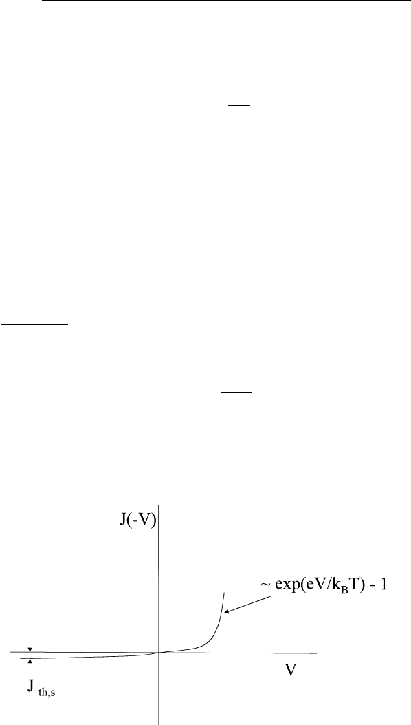
150
CHAPTER 8 / METAL–SEMICONDUCTOR INTERFACES
from the semiconductor to the metal when a voltage ⫺V is applied to
the semiconductor is given by
J(⫺V) ⫽ J
th,s
冋
exp
冉
eV
k
B
T
冊
⫺1
册
. (8.17)
The opposite case of applying a positive voltage V to the semiconductor
can be considered similarly. The corresponding result is
J(V) ⫽ J
th,s
冋
exp
冉
⫺
eV
k
B
T
冊
⫺1
册
. (8.18)
The combined result is shown in Fig. 8.13. The asymmetry in charge
transport across the interface is known as nonohmic behavior. The
particular system we discuss in this case is called a Schottky diode.
The magnitude of the Schottky barrier height determines such an asym-
metry. More rigorous treatment shows J
th,s
to be proportional to
兹
(V
BB
⫺ V). Equation (8.17) or (8.18) can be written in an approxi-
mate form as
J(⫺V) ⫽ J
o
冋
exp
冉
eV
nk
B
T
冊
⫺1
册
(8.19)
where n is known as the ideality factor. Equation (8.19) is valid only
when the magnitude of the applied voltage V « V
BB
. In this case, n ⬇
1 ⫹ (k
B
T/2eV
BB
).
FIGURE 8.13 Current versus applied voltage for a Schottky junction.
151
8.4 THE METAL–SEMICONDUCTOR INTERFACE
E
XAMPLE.
Discuss the electrical properties of a metal/n-type semi-
conductor interface when the work function of the metal is less than
that of the semiconductor using the Schottky model.
S
OLUTION.
In this case, the semiconductor bands bend downward
at the interface. This implies that the conduction band at the interface
is closer to the Fermi level than in the bulk. Since the conduction
electron concentration in a semiconductor is proportional to exp[⫺(E
CB
⫺ E
F
)/kT], this means that there is a higher conduction electron concen-
tration at the interface. Therefore, the interface is no longer a region
that limits the conductance of the metal–semiconductor system. Under
these conditions, the metal–semiconductor junction is ohmic. You may
want to practice these arguments for metal/p-type semiconductor inter-
faces.
E
XAMPLE.
Derive Eq. (8.19).
S
OLUTION.
It is given that J
th,s
is proportional to
兹
(V
BB
⫺ V)
and that V « V
BB
. The term
兹
(V
BB
⫺ V) can be approximated as
兹
V
BB
[1 ⫺ (V/2V
BB
)]. The last term can be approximated as exp(⫺
V/2 V
BB
). Incorporating this term with Eq. (8.17) gives
J(⫺V) ⫽ J
o
[exp(eV/k
B
T) exp( ⫺(V/2V
BB
)) ⫺ 1] .
The exponents can be lumped together as
eV/k
B
T ⫺ V/2V
BB
⫽ (eV/k
B
T) (1 ⫺ k
B
T / 2eV
BB
)
⬇ (eV/k
B
T))/(1 ⫹ k
B
T / 2eV
BB
)
⫽ eV/nk
B
T
where n ⫽ 1 ⫹ k
B
T/2eV
BB
.
For a given semiconductor, the foregoing model predicts that the
Schottky barrier height is equal to the work function of the metal
minus the electron affinity of the semiconductor. That is, for a given
semiconductor, a plot of the SBH versus the work function of the metal
should give a straight line with slope equal to unity. In practice, this
is not true. For example, the SBH of metal–silicon interfaces is almost
independent of the metal over a metal work function range from 4.2
to 5.7 eV. This means that the Fermi level stays practically constant
relative to the band edges. In the case of ZnO, the SBH shows some

152
CHAPTER 8 / METAL–SEMICONDUCTOR INTERFACES
dependence on the metal work function, but the slope of the plot is
still less than what is predicted by the Schottky model.
8.4.2 Surface States and the Defect Model
There is general agreement that the failure of the Schottky model to
explain the Schottky barrier results is due to the neglect of surface
states. When a metal–semiconductor junction is formed, any work
function difference between the two materials will result in an electron
flow from one material to another. Surface or interface states can act
as electron traps or sinks to pin the Fermi level. The following discussion
presents a method to estimate the surface state concentration required
to pin the Fermi level. Let us examine a specific case in which the
work function difference is 0.5 eV and the depletion width is 50 nm.
There are two regimes to consider: low and high metal coverage. For
low metal coverage, the electric field at the surface is simply equal to
0.5 V/50 nm ⫽ 1 ⫻ 10
7
V/m. From standard electrostatics, the surface
charge density is
o
E, which is equal to 8.85 ⫻ 10
⫺4
C/m
2
assuming
a dielectric constant of 10, or 5.53 ⫻ 10
15
e/m
2
. Therefore, for a surface
state degeneracy of 1 (i.e., one electron per surface state), a surface
state density of 10
15
–10
16
/m
2
would be sufficient to pin the Fermi level
at the energy position of the surface states.
On the other hand, when a thick metal layer is deposited onto the
semiconductor, electrons in the metal (in addition to those provided
by the semiconductor) can populate the surface states. This results in
an electric field on the metal side of the interface. Because of the high
electron density in a typical metal, the charge redistribution on the
metal side occurs over a small distance, typically 0.5 nm. In this case,
the electric field on the metal side is on the order of 0.5 V/0.5 nm ⫽
1 ⫻ 10
9
V/m, which is much larger than that on the semiconductor
side. Therefore, the interface charge density ⫽
o
[E(M) ⫹ E(SC)] ⬇
o
E(M), where E(M) and E(SC) are the electric fields on the metal
and semiconductor side, respectively. For the values just given, the
charge density can be shown to be about 5.5 ⫻ 10
17
/m
2
. For further
details, refer to Phys. Rev. B28, 2060 (1983) and J. Vac. Sci. Technol.
B3, 1184 (1985).
How are these surface states produced? There are two sources.
First, when metal atoms condense onto a semiconductor surface, heat
of condensation is released. When these surface metal atoms coalesce
to form a cluster, further cohesive energy is released. Such energy

153
PROBLEMS
release may disrupt the semiconductor surface and create various types
of defects, for example, vacancies, interstitials, or antisite defects. Sec-
ond, chemical reactions between the metal and the semiconductor may
occur, leading to compound or alloy formation and/or structural defects.
All these contribute to surface states that can control electronic proper-
ties of metal-semiconductor interfaces.
8.4.3 Case Study: Gold on InP
(Further reading: Phys. Rev. B32, 3904 (1985) and references therein.)
To show that massive surface disruption can occur during metal
evaporation, consider the deposition of gold onto a clean P-enriched
InP(111) surface. The P-enriched surface was prepared by heating
an argon-sputter-cleaned InP surface in 1 ⫻ 10
⫺6
torr phosphorus at
250–280⬚C. This annealing temperature was high enough to reorder
the surface after sputtering, but low enough to minimize phosphorus
evaporation from the InP surface. Gold evaporation was monitored
using a calibrated quartz crystal oscillator. The deposition rate was kept
at approximately one monolayer per minute through all experiments (1
ML ⫽ 1.2 ⫻ 10
15
gold atoms/cm
2
).
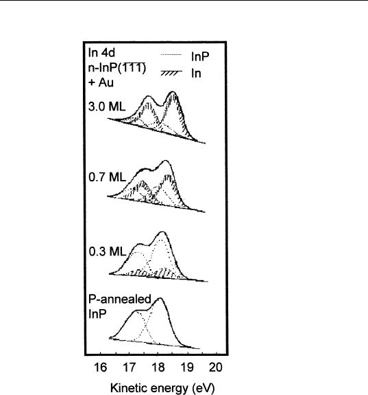
Figure 8.14 shows a series of In 4d UV photoemission spectra
from P-enriched InP as a function of gold coverage in monolayers
(ML). The peaks are decomposed into low and high kinetic energy 4d
doublets arising from indium in InP and metallic indium, respectively.
This observation is consistent with the explanation that gold deposition
results in the decomposition of InP to form metallic indium. Bulk phase
diagrams for the In–Au system indicate that formation of an In–Au
solid solution or alloy is possible. This may provide the driving force
for the decomposition of InP. Although decomposition and alloying
due to metal condensation on a semiconductor surface is by no means
a universal observation, such interactions must be considered in the
fabrication of devices involving metal–semiconductor junctions.
PROBLEMS
1. Derive Eq. (8.5).
2. Consider metal–semiconductor junctions that behave according
to the Schottky model.
154
CHAPTER 8 / METAL–SEMICONDUCTOR INTERFACES
FIGURE 8.14 In 4d photoemission spectra from P-enriched InP surface as a
function of gold coverage (hv ⳱ 40.8 eV).
(a) Draw the energy band diagram for tungsten (work function
⫽ 4.5 eV) in contact with silicon having an electron affinity
of 3.7 eV and work function of 4.0 eV.
(b) If light were to shine on this junction and create electron–hole
pairs, which way would the current flow within the device
when the junction is connected into a circuit? What would
be the maximum voltage that could be measured across the
junction (zero output load)? Explain.
Hint: The maximum voltage is obtained when no charges
are extracted from this device.
(c) Draw the energy band diagram for tungsten in contact with
silicon having a work function of 4.7 eV instead.
(d) Compare the electrical behavior of the metal–semiconductor
systems described in (a) and (c).
Hint: Consider the example in the text.

155
PROBLEMS
3. Consider an n-type semiconductor surface with acceptor surface
states located at an energy E
SS
above the valence band maximum
with a density of N
SS
states/area. By electrical neutrality, Q
SC
⫹
Q
SS
⫽ 0, where Q
SC
is the total space charge/area and Q
SS
the
total surface/area. Q
SS
is given by
(⫺eN
SS
)/[1 ⫹ exp(E
SS
⫺ E
F
)/k
B
T].
(a) What will be the corresponding expression for Q
SS
when
there are two acceptor surface states present, located at E
S1
and E
S2
with densities of N
S1
and N
S2
states/area, respectively?
(b) Extend the expression to the case of a continuous distribution
of surface states from E
a
to E
b
with a density of N
S
(E) per
unit area per unit energy range.
4. Consider the case of n-GaAs with a carrier concentration of 1 ⫻
10
17
/cm
3
and a surface state at 0.55 eV below the conduction
band on the surface. The electron degeneracy of this surface state
is 2. You can assume that the Fermi level in the bulk of n-GaAs
at this doping concentration coincides with the conduction band
minimum. The dielectric constant of GaAs is 12.
Based on the preceding information, make a plot of the band
bending at 300 K as a function of the density of surface states
N
SS
from zero to 1 ⫻ 10
13
/cm
2
. You should find that the Fermi
level is pinned at a surface state density of less than 1 ⫻ 10
13
/
cm
2
. What is the energy position of the pinned Fermi level with
respect to the conduction band minimum?
5. Consider a 1-m-thick n-type semiconductor film deposited on
an inert substrate. The semiconductor carrier concentration is 1
⫻ 10
18
/cm
3
. For simplicity, let us assume that there are no surface
states. This film is exposed to a certain gas adsorbate, which acts
as an electron acceptor. Some mobile electrons in the semiconduc-
tor film are captured by the adsorbate species, and the film resis-
tance increases. Assuming that one monolayer of this adsorbate
removes 1 ⫻ 10
13
electrons/cm
2
, what is the fractional change
in film resistance? This phenomenon is the basis for gas sensors.

156
CHAPTER 8 / METAL–SEMICONDUCTOR INTERFACES
APPENDIX
USEFUL INFORMATION FOR SEMICONDUCTORS
Electron concentration n ⫽ N
c
exp[⫺(E
CB
⫺ E
F
)/kT]
Hole concentration p ⫽ N
v
exp[⫺(E
F
⫺ E
VB
)/kT]
Si GaAs
Atomic weight 28.1 144.6
Lattice constant (nm) 0.543 0.565
Density (g/cm
3
) 2.33 5.32
Energy gap (eV) 1.11 1.40
N
c
(/cm
3
) 2.8 ⫻ 10
19
4.7 ⫻ 10
17
N
v
(/cm
3
) 1.04 ⫻ 10
19
7.0 ⫻ 10
18
Intrinsic carrier concentration (/cm
3
) 1.45 ⫻ 10
10
9 ⫻ 10
6
Intrinsic mobilities (cm
2
/V-s)
Electrons 1350 8600
Holes 480 250
Dielectric constant 11.7 12
Melting point (⬚C) 1415 1238
Thermal conductivity (W/cm K) 1.5 0.81
Specific heat (J/g K) 0.7 0.35
Thermal expn. coeff. (/K) 2.5 ppm 5.9 ppm