Chung Y.-W. Practical guide to surface science and spectroscopy
Подождите немного. Документ загружается.


8
METAL–SEMICONDUCTOR
INTERFACES
8.1 SURFACE STATES
In bulk band structure calculations, it is always assumed that the solid
exhibits three-dimensional translational symmetry. The wavefunction
for the electron, labeled by (n,k) where n is the band index and k the
electron wave vector, can be expressed in the form
n,k
(r) ⫽ u
n,k
(r)exp(ik ⭈ r) , (8.1)
where u
nk
(r) has the same periodicity as the lattice and k is real.
However, the solid is not infinite, but is bounded by surfaces and hence
does not have three-dimensional translational symmetry. Surface atoms
are in an environment markedly different from their bulk counterparts.
They may relax to new positions and cause perturbations to atoms in
the second and subsequent layers. That is, the periodic potential is
perturbed perpendicular and parallel to the surface. Electron wavefunc-
tions near the surface will still have the form of Eq. (8.1), except that
the periodicity is restricted to the two dimensions parallel to the surface
137
138
CHAPTER 8 / METAL–SEMICONDUCTOR INTERFACES
and that k can be complex. These wavefunctions can be classified into
two types: (1) surface resonance—the wavefunction is bulklike inside
the solid and decays exponentially from the surface to vacuum; (2)
true surface state—the wavefunction decays to zero on both sides of
the surface. Electronic states described by these wavefunctions are
broadly referred to as surface states.
Surface states that occur on a clean surface are termed intrinsic
surface states, and states associated with adsorbates are called extrinsic
states.
Let us examine these surface states using a standard one-dimen-
sional treatment. First, the Schro
¨
dinger equation describing an electron
wave function moving in a potential V(z) is given by
冋
⫺
d
2
dz
2
⫹ V(z)
册
(z) ⫽ E
(z) (8.2)
where ប
2
/2m ⫽ 1 for simplicity. We assume that the potential is given
by
V(z) ⫽⫺V
o
⫹ 2V
g
cos gz (8.3)
where g ⫽ 2/a is the shortest reciprocal lattice vector of the chain.
Equation (8.2) can readily be solved using the following trial wave-
function:
k
(z) ⫽ A exp(ikz) ⫹ B exp[i(k ⫺ g)z]. (8.4)
Substituting this and Eq. (8.3) into Eq. (8.2) gives the actual wave-
functions and energy values:
E ⫽⫺V
o
⫹
g
2
4
⫹ K
2
⫾ 兹g
2
K
2
⫹ V
2
g
(8.5)
⫽ e
ikz
cos
冉
gz
2
⫹
␦
冊
where exp (2i␦) ⫽ (E ⫺ k
2
)/V
g
and K ⫽ k ⫺ g/2.
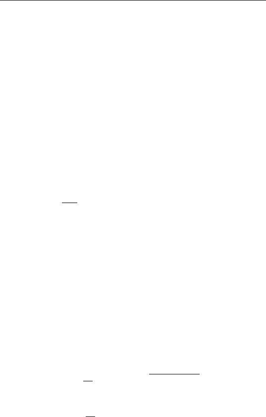
A plot of the energy function E(K
2
) versus K
2
is shown in Fig.
8.1. There is the usual energy gap at K ⫽ 0, the zone boundary.
Note that E can be a continuous function of K
2
if we allow negative
values of K
2
, that is, imaginary values of K. In the bulk, these solutions
are not allowed because they lead to infinite wave amplitudes as 兩z兩
approaches infinity.
139
8.1 SURFACE STATES
FIGURE 8.1 E versus K
2
for a one-dimensional solid near the Brillouin zone
boundary. (Adapted from Andrew Zangwill, Physics at Surfaces, Cambridge University
Press.)
On the other hand, consider the case in which we terminate a solid
with a surface as shown in Fig. 8.2, as represented by a surface potential
with height V
o
at z ⫽
1
–
2
a. Outside the surface (i.e., z ⬎
1
–
2
a), the wave-
function is simply given by
⬎
(z) ⫽ e
⫺qz
, where q
2
⫽ V
o
⫺ E. Inside
FIGURE 8.2 Potential variation and electron wavefunction near the solid surface.
(Adapted from Andrew Zangwill, Physics at Surfaces, Cambridge University Press.)
140
CHAPTER 8 / METAL–SEMICONDUCTOR INTERFACES
the surface (i.e., z ⬍
1
–
2
a), we can accept imaginary values of K by
writing K ⫽ iQ. Therefore, we have
⬎
(z) ⫽ exp(⫺qz) for z ⬎ a/2 (8.6a)
⬍
(z) for z ⬍ a/ 2. (8.6b)
⫽ exp(Qz)cos
冉
gz
2
⫹ ␦
冊
At z ⫽
1
–
2
a, we require the wavefunction and its derivative to be continu-
ous. If these requirements are satisfied, then a surface state exists with
energy Q
2
.
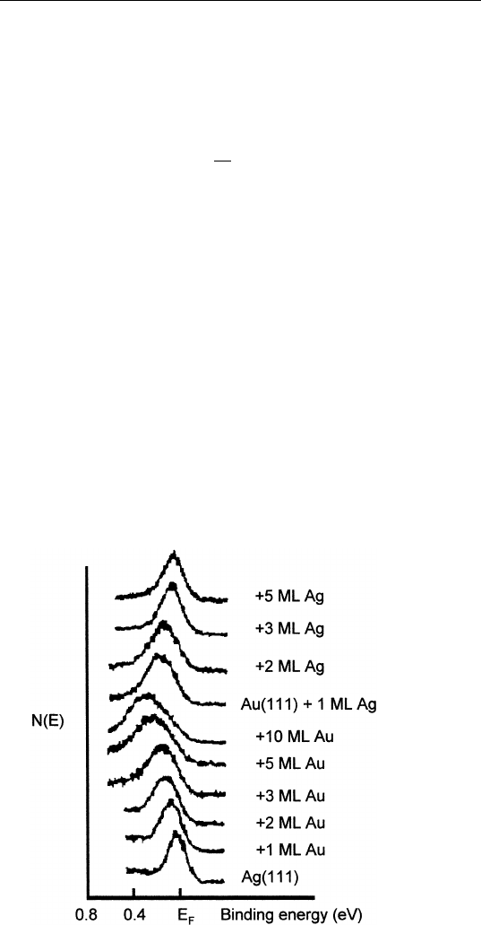
Note from Eq. (8.6) that the surface state is localized to a distance
within 1/q of the surface. One can study this localization using photo-
electron spectroscopy. To be specific, consider a Ag(111) surface. When
one performs photoemission at normal electron exit, one observes a
surface state peak just below the Fermi level (Fig. 8.3). As one grows
gold epitaxially on the Ag(111) surface, the surface state peak evolves
continuously to one located at 0.35 eV below the Fermi level, due to
a surface state in Au(111). This evolution can be analyzed as follows.
One first writes down the Schro
¨
dinger equation for Ag and Au:
H(t)
i
⫽ E
i
i
, i ⫽ 1, 2 (Ag, Au) . (8.7)
FIGURE 8.3 Shift of the surface state energy position for Ag/Au(111) versus film
thickness. (Reprinted from T. C. Hsieh and T. C. Chiang, Surf. Sci. 166, 554 (1986).)
141
8.2 SEMICONDUCTOR SURFACES
For material 2 with thickness t on material 1, one can write
H(t)(r,t) ⫽ E(t)(r,t) (8.8)
where (r,t) should have the form of Ae
⫺qz
. From Feynman’s theorem,
we have
dE(t)
dt
⫽
冕
*
dH
dt
d
3
r . (8.9)
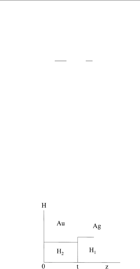
From Fig. 8.4, it is easy to see that dH(t)/dt for an abrupt epitaxial
interface can be set to a delta function ␦(z ⫺ t) so that the right-hand-
side of Eq. (8.9) is simply (E
1
⫺ E
2
) ⫻ exp(⫺2qt). Therefore, the
surface state peak position shifts with film thickness t exponentially.
From the observed shift as a function of thickness, one can determine
1/q, the spatial extent of the surface state wavefunction perpendicular
to the surface. Experimentally, 1/q is found to be about one monolayer.
For additional information, refer to the article by Hsieh et al., Phys.
Rev. Lett. 55, 2483 (1985).
8.2 SEMICONDUCTOR SURFACES
8.2.1 The Space Charge Region
Consider an n-type semiconductor at thermal equilibrium at temperature
T above absolute zero. All electronic levels are populated in the usual
way. The semiconductor crystal is then cleaved to produce a fresh
FIGURE 8.4 Schematic diagram showing the energy variation at the Ag/Au inter-
face.
142
CHAPTER 8 / METAL–SEMICONDUCTOR INTERFACES
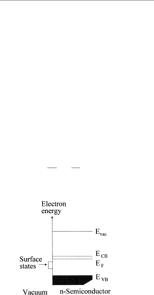
surface, which introduces surface states localized at the surface. Let
us assume that there is a band of such states localized somewhere in
the gap below E
F
, as shown in Fig. 8.5. If these surface states are
unoccupied, the system will not be at thermal equilibrium. To achieve
thermal equilibrium, electrons must flow from the bulk of the semicon-
ductor to the surface to fill up these states. As these states are filled,
an electric field is set up that opposes electron flow to the surface.
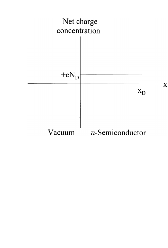
Assume that at equilibrium, the total electron charge at the surface is
Q
SS
C/cm
2
. For an n-type semiconductor with a donor concentration
of N
D
/cm
3
, this requires surface depletion of conduction electrons over
a thickness of x
D
⫽Q
SS
/eN
D
, thus creating a surface electrostatic dipole.
For Q
SS
⫽10
12
e/cm
2
and N
D
⫽ 10
17
/cm
3
, x
D
⫽ 1⫻10
⫺5
cm, or 100
nm. This surface region in which mobile charge carriers are depleted
(in order to fill the surface states) is known as the surface space charge
or depletion region (Fig. 8.6).
Because of this dipole field, there is a potential energy difference
between, say, a conduction electron in the bulk and one on the surface.
This variation as a function of distance in the space charge region can
be obtained by solving the Poisson equation,
d
2
V
dx
2
⫽⫺
0
, (8.10)
where V is the potential, the charge density, the dielectric constant,
and
o
permittivity of free space (⫽ 8.8 ⫻ 10
⫺12
F/m).
FIGURE 8.5 Nonequilibrium energy diagram for an n-type semiconductor/vacuum
interface.
143
8.2 SEMICONDUCTOR SURFACES
FIGURE 8.6 Charge distribution at a vacuum/n-semiconductor interface.
A commonly adopted approach to the solution of Eq. (8.10) is to
use the depletion approximation. The depletion approximation states
that for x ⬎ 0 (inside the semiconductor),
(0 ⬍ x ⬍ x
D
) ⫽ eN
D
(8.11)
(x ⬎ x
D
) ⫽ 0.
Putting V(x
D
) ⫽ 0 as the boundary condition, we can solve Eq. (8.10)
to give
V(x) ⫽⫺
eN
D
(x ⫺ x
D
)
2
2
0
. (8.12)
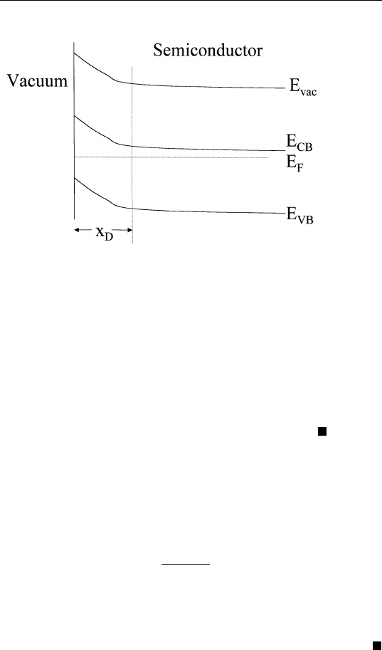
At x ⫽ 0 (the semiconductor surface), the potential energy of an electron
relative to the bulk of the semiconductor is equal to (-e)V(0) ⫽ e
2
N
D
x
D
2
/(2
0
). The energetics are shown in Fig. 8.7. Several features
should be noted:
(a) The Fermi level is flat throughout, since the system is as-
sumed to be in equilibrium.
(b) The upward bending of all the bands toward the surface
implies that in equilibrium, it is difficult for electrons from the
bulk to move to the surface.
144
CHAPTER 8 / METAL–SEMICONDUCTOR INTERFACES
FIGURE 8.7 Equilibrium energy band diagram for a vacuum/n-semiconductor
interface.
(c) All bands bend up by the same amount, indicating that both
the bandgap (E
CB
⫺ E
VB
) and the electron affinity (E
VA C
⫺
E
CB
) are not affected by surface states.
Q
UESTION FOR
D
ISCUSSION.
In practice, the depletion approxima-
tion turns out to be an excellent approximation. Why?
The energy difference between an electron at the conduction band
minimum at the surface and the counterpart in the bulk is 兩eV(0)兩 and
is called band bending eV
BB
. Since Q
SC
⫽ eN
D
x
D
(the space charge
density),
eV
BB
⫽
Q
2
SC
2
0
N
D
. (8.13)
Q
UESTIONS FOR
D
ISCUSSION.
How will the band bending be differ-
ent for a p-type semiconductor? How will high doping concentration
affect the width of the depletion region and the band bending?
8.2.2 Fermi-Level Pinning
Consider an n-type semiconductor with surface states of density N
SS
(E)
states per unit area per energy interval in the band gap, located between
E
SS
and E
SS
⫹ ⌬ above the valence band maximum, as shown in Fig.
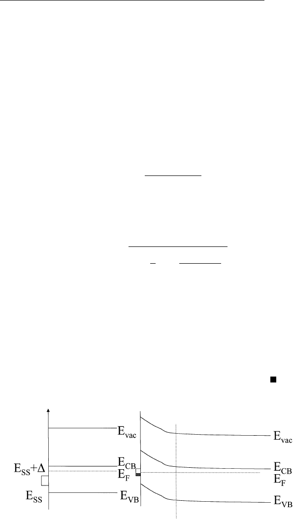
145
8.2 SEMICONDUCTOR SURFACES
8.8. When the surface charge is Q
SC
C/cm
2
, this means that the surface
states are filled up to an energy of E
SS
⫹ Q
SC
/eN
SS
above the valence
band maximum, through which the Fermi level at the surface must
intersect. If the density of surface states N
SS
(E) is sufficiently large so
that Q
SC
/eN
SS
is negligible, the Fermi level will essentially be fixed
(or pinned) at the energy position of the surface states (E
SS
) above the
valence band maximum.
A rigorous treatment goes as follows. At thermal equilibrium, the
charge Q
SC
in the space charge region and the charge Q
SS
in surface
states must balance each other, that is, Q
SC
⫹ Q
SS
⫽ 0. From Eq.
(8.13) for an n-type semiconductor,
Q
SC
⫽ 兹
2
0
N
D
eV
BB
. (8.14)
The charge residing in acceptor-like surface states of energy E
SS
must
obey the Fermi–Dirac distribution function, as follows:
Q
SS
⫽ eN
SS
1
1 ⫹
1
g
exp
冉
E
SS
⫺ E
F
k
B
T
冊
. (8.15)
Here, N
SS
is the density of surface states and g is the degeneracy factor
(i.e., the number of electrons occupying one surface state). The surface
state is assumed to be located at E
SS
above the valence band maximum.
From Eqs. (8.14) and (8.15), the variation of band bending as a function
of N
SS
for a given surface state can be calculated.
Q
UESTION FOR
D
ISCUSSION.
Using Eq. (8.14) and (8.15), deter-
mine the band bending as a function of N
SS
graphically.
FIGURE 8.8 Illustration of Fermi–level pinning by surface states.
146
CHAPTER 8 / METAL–SEMICONDUCTOR INTERFACES
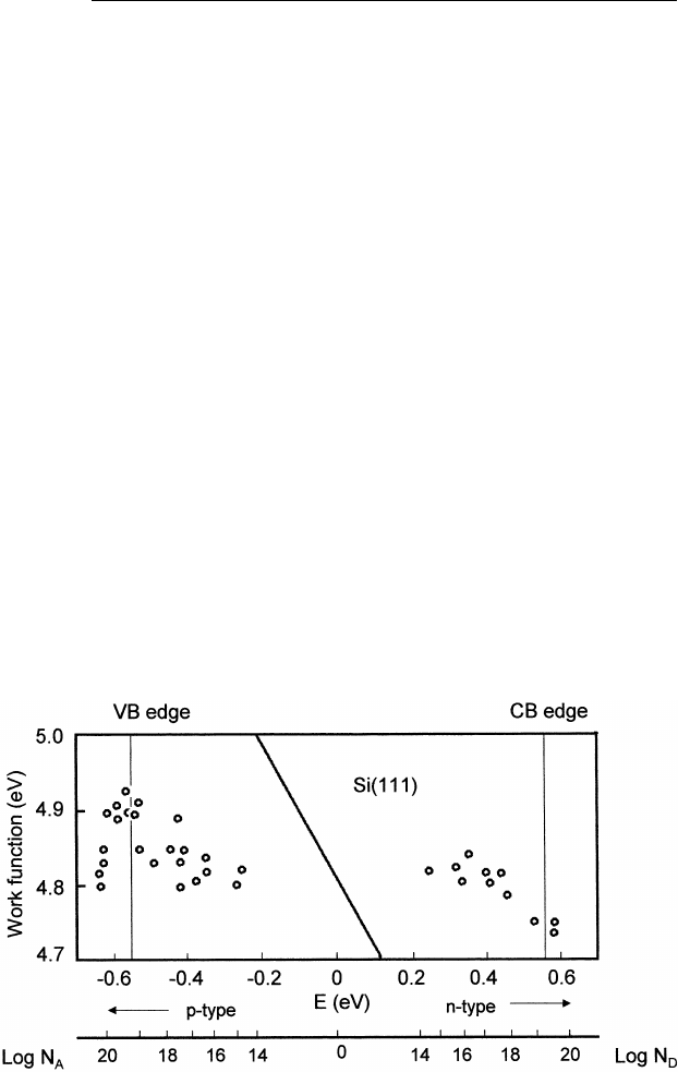
The effect of surface states on Fermi level pinning is shown in
Fig. 8.9 for Si(111). In this case, a clean Si(111) surface is produced
by cleavage in ultrahigh vacuum. The work function is measured for
different doping levels. The straight line indicates the expected behavior
from the shift of the Fermi level due to doping if no surface states
were present. Over the doping range of 1 ⫻ 10
18
/cm
3
p-type to 1 ⫻
10
18
/cm
3
n-type, the work function is constant at about 4.8 eV. This
implies that the Fermi level is pinned by surface states located at about
0.6 eV below the conduction band minimum (electron affinity for Si
⫽ 4.2 eV).
8.3 WORK FUNCTION MEASUREMENTS
The preceding example demonstrates the power of work function mea-
surements to show the existence of surface states on semiconductor
surfaces. It is also one of the first publications on the detection of
surface states (see the original article by Allen and Gobeli, Phys. Rev.
127, 152 (1962)). We now take a short digression to discuss three
standard methods of work function measurement.
FIGURE 8.9 Variation of work function of cleaved Si(111) as a function of bulk
doping. (Adapted from Andrew Zangwill, Physics at Surfaces, Cambridge University
Press.)