Buschow K.H.J. (Ed.) Concise Encyclopedia of Magnetic and Superconducting Materials
Подождите немного. Документ загружается.

of magnitude difference in commitments of time, per-
sonnel and funds to the two fields since the mid-1940s,
which are themselves measures of the relative com-
mercial importance of the two fields to date. Some
superconducting devices can be made in a single film
of material, the most common uses two films and the
most complex requires only three. Despite this, they
perform logic functions faster than the most advanced
semiconductor devices and at a level of power dissi-
pation which is orders of magnitude smaller (see Thin
Films, Multilayers and Devices, Superconducting).
Whether they will ever become more complex, or in-
deed need to do so, is an open question.
3.1 Tunnel Junctions and Weak Link Structures
Superconductors are affected strongly by magnetic
fields and only weakly by electric fields. This mag-
netic field sensitivity is the basis for many electronic
devices. In a superconducting film, or film adjacent to
a superconductor, a local region is produced where
the superconducting state can be controlled by ex-
ternal magnetic fields. The cryotron (Buck 1956),
which was the earliest superconducting electron de-
vice, used this principle. This device, which was in-
vented in 1954 and therefore predates the Josephson
effect, used two films (see Fig. 6) separated by an
insulator. A current through the control film created
a magnetic field which switched the second film from
its superconducting to its normal state. Recovery
from the normal state was not fast (by modern
standards). With the discovery of the Josephson
effect (see Josephson 1962) a much faster device be-
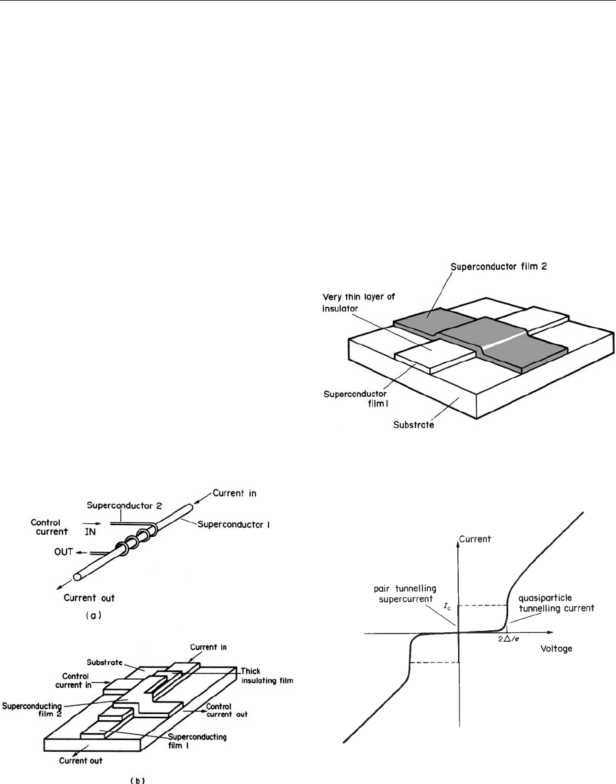
came possible. The Josephson junction (see Fig. 7)
consists of two superconducting films separated by a
thin insulator (o1.5 nm thick). This insulator allows
the tunnelling of pairs of electrons (the Josephson
current) and single electrons (the quasiparticle cur-
rent). These result in the tunnelling currents shown in
Fig. 8 as a function of the voltage across the insu-
lator. For an ideal junction there would be a discon-
tinuous jump at 2D/e and an exponentially small
subgap tunnelling current proportional to exp(D/
k
B
T) (Van Duzer and Turner 1981). In real systems
there is a smearing due to lifetime effects and non-
uniformity in the films. In addition there is invariably
a subgap leakage current. The sources of subgap
leakage vary from device to device and depend very
Figure 6
Cryotron types: (a) wire-wound type, (b) thin-film type.
Figure 7
Josephson junction (SIS tunnel junction).
Figure 8
I–V characteristic of Josephson junction for the case
where the two superconducting films have the same
energy-gap parameter D, the characteristic shows some
subgap leakage current.
1240
Thin Films, Multilayers and Devices, Supercondu cting
much on the fabrication of the device. Leakage can
for instance arise from electron states within the tun-
nel barrier, or pinholes in the barrier itself. At low
temperatures for very-high-quality low-leakage bar-
riers, small subgap currents due to two-particle or
many-particle tunnelling can be observed (Kirk et al.
1991). If a small magnetic field is applied to the junc-
tion parallel to the films, the Josephson current is
reduced to zero when one quantum of magnetic flux
is in the area given by the width of the junction mul-
tiplied by the sum of the London penetration depths
of the two films (Rowell 1963). In practical devices,
this is about 0.1–1 mT. It is important to realize that,
in contrast to the cryotron, it is only the Josephson
current that is switched off by the magnetic field. The
two films comprising the junction remain entirely su-
perconducting at these low magnetic fields. In addi-
tion to control by magnetic field, the junction can
also be switched by increasing the current until the
maximum Josephson current is exceeded.
The Josephson tunnel junction has become the de-
vice of choice for LTS electronic, instrument and
sensor applications (Ruggiero and Rudman 1990). It
is fast and consumes little power. Its modern form,
made from Nb/Al–Al oxide–Nb, is described in detail
in SQUIDs; Biomedical Applications; SQUIDs: The
Instrument; Josephson Voltage Standard; Josephson:
Junctions: Low-T
c
Soon after the theoretical discovery and experi-
mental verification of the Josephson tunnel junction,
it was realized that Josephson effects could be ob-
served in many even simpler structures, which are
now collectively known as weak links (Anderson and
Dayem 1964). No tunnelling occurs in any of these
structures, they rely instead on creating a region of
weak coupling between two superconductors by var-
ious means other than an oxide layer. Some examples
are shown in Fig. 9. The simplest is a contact between
a pointed wire of one superconductor and a second
bulk superconductor (‘‘point contact’’). The thin-film
version is a small constriction defined in a film
(a ‘‘weak link’’, ‘‘bridge’’ or ‘‘microbridge’’). A ‘‘var-
iable thickness bridge’’ has the constriction both
thinner and narrower than the surroundings (banks).
The coupling region can also be made from a normal
metal, which is made weakly superconducting by the
proximity effect (SNS junction).
In all these Josephson weak link devices, the length
of the coupling region must be comparable to the
superconducting coherence length in that region. In
LTS materials and normal metals, standard film
growth and lithographic techniques can produce fea-
tures of the sizes required (generally t1 mm). In HTS
materials, this is obviously not possible.
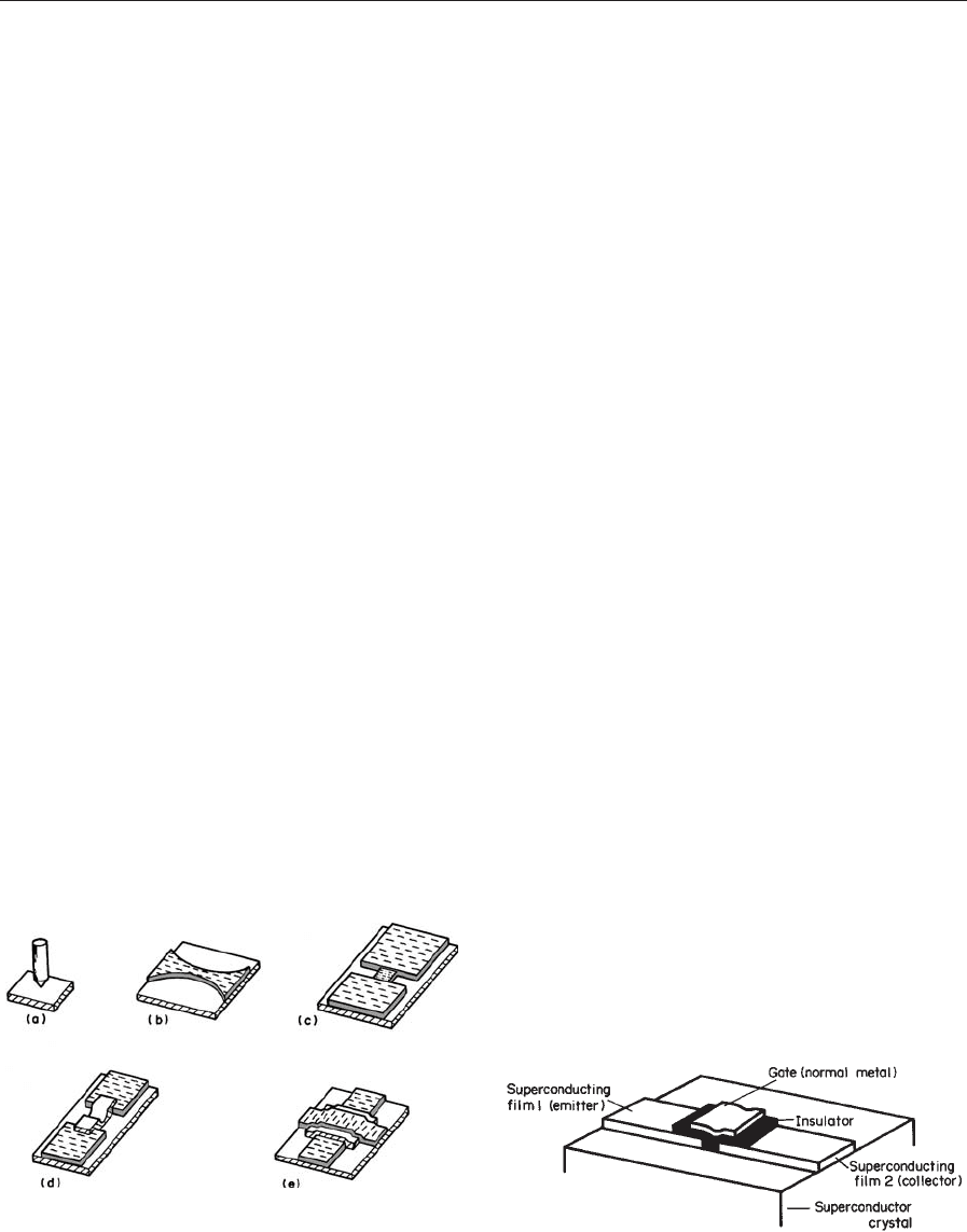
Unlike the semiconducting transistor, supercon-
ducting devices do not have gain. At a fixed current
level, they simply switch between the zero voltage and
finite voltage states with application of magnetic field.
A few three-terminal devices have been investigated
that are more transistorlike in design, but not yet in
operation (Kleinsasser and Gallagher 1990). One ex-
ample is the superconducting FET (see Fig. 10), in
which two closely spaced superconducting contacts
induce a weak coupling region on the surface of a
semiconductor by the proximity effect. This super-
conducting channel is then switched on and off by
application of an electric field from the gate. To date,
large gate voltages are required to achieve switching
and the devices are not practical.
As of mid-1991, the device scene in HTS materials
is one of great activity and some uncertainty. All the
devices made in LTS materials are being investigated,
with varied levels of success. It is clear that the short
coherence lengths of the HTS materials creates a real
challenge in device design and processing. It does
seem likely that junctions of the weak link type will
emerge as more important than tunnel junctions, at
least in those HTS materials with T
c
477 K. The rea-
sons for this will be given later.
One HTS device has been created which has no
LTS counterpart. A control line modulates the flux
density in a weakened region of a second film (chan-
nel). It can be called a flux-flow cryotron (Martens
et al. 1991) in that the channel is switched from zero
resistance into its flux flow state, rather than into its
normal state. Its value in interface circuits has already
Figure 9
Josephson weak link structures: (a) point contact, (b)
constriction, (c) variable thickness bridge, (d) SNS
planar and (e) SNS sandwich.
Figure 10
Superconducting three-terminal device (FET type).
1241
Thin Films, Multilayers and Devices, Superconducting
been demonstrated, in that its output voltage is quite
large (tens to hundreds of millivolts).
3.2 Device Processing: LTSs
The LTS weak link devices are relatively easy to
make with current lithographic techniques. Optical,
electron-beam and ion-beam patterning have all been
used to create the weak regions of dimensions 1 mmor
less in a variety of materials. The details will not be
discussed here.
Tunnel junctions exhibiting quasiparticle tunnel-
ling were first made in the late 1950s by the very
simple process of evaporating a strip of aluminum
film using a shadow mask, exposing it to the air for a
short time (B1 min), then evaporating a crossing
strip of lead to produce an Al–Al oxide–Pb tunnel
junction (Giaever 1960). The brief exposure to air
grows the required thickness of aluminum oxide
(B1.5 nm) which completely covers the aluminum
film even over relatively large areas of a few square
millimeters. It is important that there are no defects
or ‘‘pinholes’’ in the oxide, otherwise a metallic short
circuit occurs. This basic oxidation process has been
used for the vast majority of tunnel junctions made
on many different materials, and is used in the cur-
rent commercial process.
Other materials that have been used to make oxide
tunnel junctions include lead, tin, niobium, tantalum
and the alloys and A15 compounds of niobium. In
some cases the oxidation is not so easy as it is for
aluminum and heating in oxygen is required. Because
of its relatively high T
c
(7.2 K), lead and its alloys
received many years of study as the metallizations for
Josephson circuits. The problems that were encoun-
tered illustrate the difference between the research
mode of making a few successful junctions for scien-
tific study, and a manufacturing mode of rep-
roducibly making circuits that require many
thousands of junctions. The variation of critical cur-
rent density across these junctions must be small and
they must survive both shelf storage and many ther-
mal shocks as they are cycled from 300 K to 4.2 K
and back to 300 K. Because of the failure of lead, no
satisfactory metallization for Josephson circuits ex-
isted for 20 years (1963–1983). Niobium was an ob-
vious choice (T
c
¼9.2 K), but oxidation of niobium
itself produces a mixture of oxides with insulating,
semiconducting and even metallic properties. There is
probably also degradation of the niobium film sur-
face. This problem was finally solved by immediately
depositing a thin layer (o10 nm) of aluminum on top
of the niobium film in the same vacuum system, then
oxidizing the aluminum to form an aluminum oxide,
rather than niobium oxide, tunnel barrier (Geerk
et al. 1982).
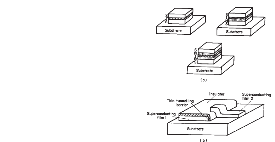
Such ‘‘artificial’’ barriers have been used for a
number of other materials that do not readily oxidize
themselves. The best known example is MgO, which
is deposited as a thin layer on top of NbN to form
NbN–MgO–NbN tunnel junctions (Shoji et al. 1985).
The different types of ‘‘sandwich’’ tunnel junctions
are shown in Fig. 11.
The sizes of sandwich junctions can be as small as
1 mm 1 mm using standard optical lithography and
submicrometer sizes using deep-UV sources. Another
way to make very small junctions is to oxidize the
edge of a film that has been cut by ion milling. Such
an ‘‘edge junction’’ is shown in Fig. 11. The small
capacitance of such structures makes them suitable
for high-frequency SIS detectors used in radio as-
tronomy studies.
3.3 Device Processing: HTSs
The new oxide materials with T
c
477 K are demand-
ing the invention of a new device technology. They
readily form tunnel junctions with counterelectrodes
of low-T
c
materials (Geerk et al. 1988), either because
their surfaces lose oxygen and become insulating, or
because the counterelectrode itself (e.g., lead) removes
the oxygen to form the insulator. However, such
junctions have no technological value. Obviously
there is no Josephson current until the temperature
is below T
c
of the counter electrode and, at least to
date (1991), none of them exhibits the I–V character-
istic of Fig. 8 with well-defined Josephson current
and energy gap. This comment applies to all the
Figure 11
(a) Three types of multilayer sandwich structure
Josephson junction, SIS, SNIS and SNINS; (b) edge-
type Josephson junction.
1242
Thin Films, Multilayers and Devices, Supercondu cting
anisotropic oxides. Whether it is an intrinsic property
remains to be seen.
The isotropic oxides (e.g., BaPbBi oxide, BaKBi
oxide) are strikingly different. A ‘‘classical’’ I–V
characteristic of the type shown in Fig. 8 has been
observed by simply touching a BKBO single crystal
to a BKBO film and work is underway to produce
similar results in a thin-film sandwich structure. At
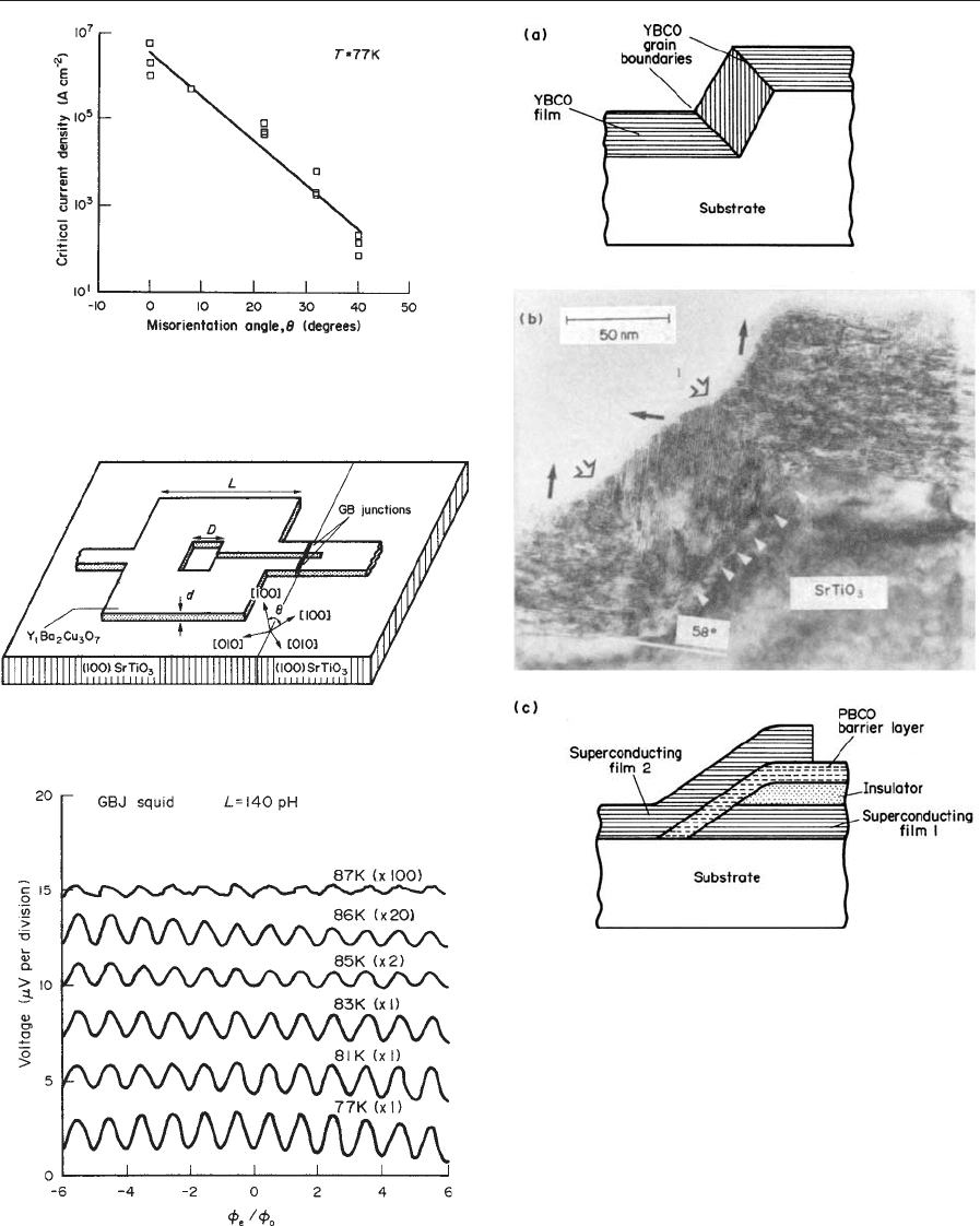
Figure 12
Variation of critical current density with misorientation
angle for grain boundaries in YBCO films on yttria-
stabilized zirconia (YSZ) substrates.
Figure 13
Bicrystal SQUID structure with grain boundary
junctions.
Figure 14
Field modulation of bicrystal SQUID illustrated in Fig.
13 for temperatures between 77 K and 87 K.
Figure 15
(a) Schematic of steep step junction with two grain
boundaries, (b) electron micrograph of 581 step junction
in a YBCO film on SrTiO
3
(after Jia et al. 1991) and
(c) schematic of a shallow step junction with a normal
PrBCO layer.
1243
Thin Films, Multilayers and Devices, Superconducting
present, the maximum T
c
in an isotropic oxide su-
perconductor is about 30 K. However, this would al-
low a Josephson technology similar to that developed
for niobium to be used at 12–15 K, well within the
range of closed cycle refrigerators of reasonable cost.
Thus, these isotropic oxides might become important
metallizations for electronics applications.
In the absence of any useful tunnel junctions in
HTS materials, the weak link devices are of more
importance than they were in the LTS field (although
it is true that most of the SQUID-based LTS mag-
netometers that have been sold have in fact used such
weak links rather than tunnel junctions). A great va-
riety of device structures are being investigated at
present (mid-1991). Many of them make SQUIDs
operating at 77 K. Whether any of them will become
the basis of a genuine circuit technology remains to
be seen. They include SNS devices where the N layer
can be silver (or silver–gold alloy). In one geometry
the silver covers a break in the HTS film induced by a
step in the substrate. Other N layers are semicon-
ducting and ‘‘metallic’’ oxides, in various geometries
(Simon 1991). The possible presence of a proximity
effect in such oxides is an interesting issue.
To define a weak link constriction, or region of
reduced J
c
and T
c
, of a size comparable to the very
short coherence lengths, is difficult in HTS materials.
However, electron-beam writing and focused ion-
beam milling have been used with some success, and
the use of patterning by a scanning tunnelling mi-
croscope has been proposed. In one structure nature
itself seems to provide a structure of the correct di-
mensions, namely a boundary between two grains in
the film. The cleanest examples of such devices are
grain boundary junctions grown on substrates that
were cut and deliberately misaligned in the plane by
Figure 16
The density of filled and empty quasiparticle states for lead and tin superconducting layers on each side of a tunnel
barrier. An applied voltage V leads to a relative displacement of the density of state diagrams, the voltage
corresponding to the gap 2D is 2D/e: (a) zero applied voltage; (b) eV ¼D
Pb
D
Sn
C0.8 mV; (c)
D
Pb
D
Sn
oeVoD
Pb
þD
Sn
, eVC1.4 mV; and (d) eV ¼D
Pb
þD
Sn
C2.0 mV.
1244
Thin Films, Multilayers and Devices, Supercondu cting
various tilt angles (Gross et al. 1990a). The film,
growing epitaxially, replicates the orientation of the
substrate. On yttria-stabilized zirconia substrates, the
critical current drops exponentially with angle, by
four orders of magnitude as the angle is increased
from 0 to 401 (see Fig. 12) (Ivanov et al. 1991).
SQUIDs of YBCO showing modulation with mag-
netic field up to 87 K have been produced with such
grain boundary junctions (Gross et al. 1990b). (See
Fig. 13, which shows the structure, Fig. 14 demon-
strating the modulation and also the article Josephson
Junctions: High-T
c
.)
A step geometry has also been used to form weak
link HTS junctions (see Fig. 15). If the angle of the step
is steep (y4451) single or multiple grain boundaries
form at the discontinuity in the substrate surface
(Fig. 15a,b). For shallow junctions (yo351)theepitaxy
is preserved at the step and an SNS junction can be
formed by depositing a heteroepitaxial layer of normal
PrBCO (Fig. 15c) (Gao et al. 1991). In this junction
films are grown with the c axis normal to the substrate
so that the tunnelling current is in the ab plane, the
direction with longest coherence length.
An alternative process called biepitaxy creates a
grain boundary in the film by control of the in-plane
epitaxy using seed and buffer layers (Char et al.
1991a), rather than by changing the substrate orien-
tation. This process could allow complex circuits of
grain boundary junctions to be demonstrated, as the
junction can be located at any point on a single-crys-
tal substrate. The first integrated SQUID magneto-
meter fabricated on one chip used such biepitaxial
grain boundary junctions (Char et al. 1991b).
3.4 Properties of Devices
The ideal BCS current–voltage characteristic of LTS
tunnel junctions can be readily understood by the use
of semiconductorlike diagrams in which the filled and
empty quasiparticle states are shown at an energy 2D
apart and have (E
2
D
2
)
1/2
energy dependencies of the
density of states (see Fig. 16). The superconducting
pairs are shown at the Fermi level, the midpoint of
the gap. The effect of an applied voltage V is simply
to slide the Fermi levels and thus the whole gap
structures relative to each other by a distance eV. The
effect of temperature is included by a thermal distri-
bution over only the quasiparticle states.
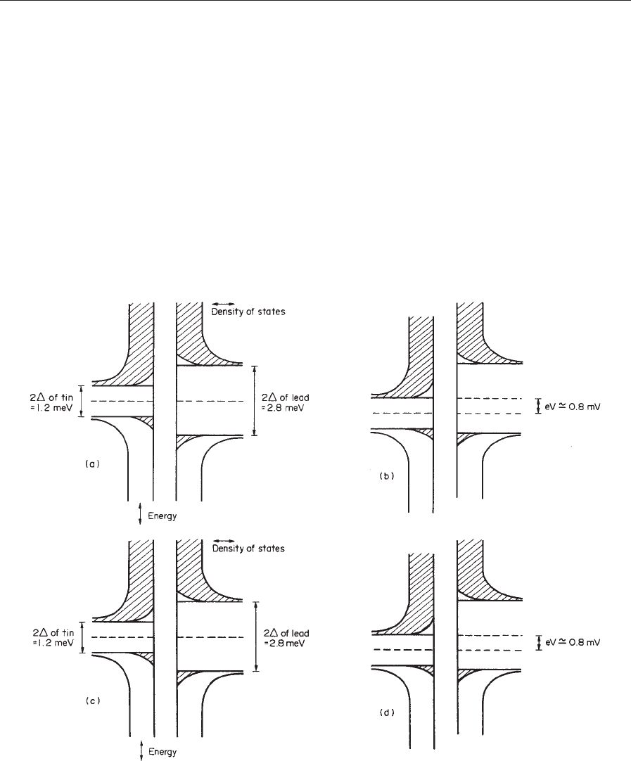
The most interesting case is that of two supercon-
ductors with different energy gaps, say tin and lead to
be specific. The T
c
values are 3.7 K and 7.2 K, and the
energy-gap parameters D ¼0.6 meV and 1.4 meV, re-
spectively or 2D ¼1.2 meV and 2.8 meV. The density
of states diagrams are then as shown in Fig. 16a at
zero voltage and a temperature significantly below
the T
c
of tin. As the voltage is increased, a maximum
in current occurs at eV ¼D
Pb
D
Sn
(Fig. 16b), but the
current then decreases for larger voltages. This is
because the current is the integral over the filled and
empty states that are aligned with each other, which
is smaller in Fig. 16c than in Fig. 16b. A sudden
increase in current occurs for eV ¼D
Pb
þD
Sn
in
Fig. 16d. In theory, this should be a discontinuous
Figure 17
The current–voltage characteristic for the tunnelling of
quasiparticles in an Sn–I–Pb junction.
Figure 18
SIN tunnel junction: (a) density of filled and empty
states at zero applied voltage, and (b) current–voltage
characteristic at finite temperature.
1245
Thin Films, Multilayers and Devices, Superconducting
jump in current at any temperature, but in practice it
has a slight width due to lifetime effects and nonuni-
formities in the films.
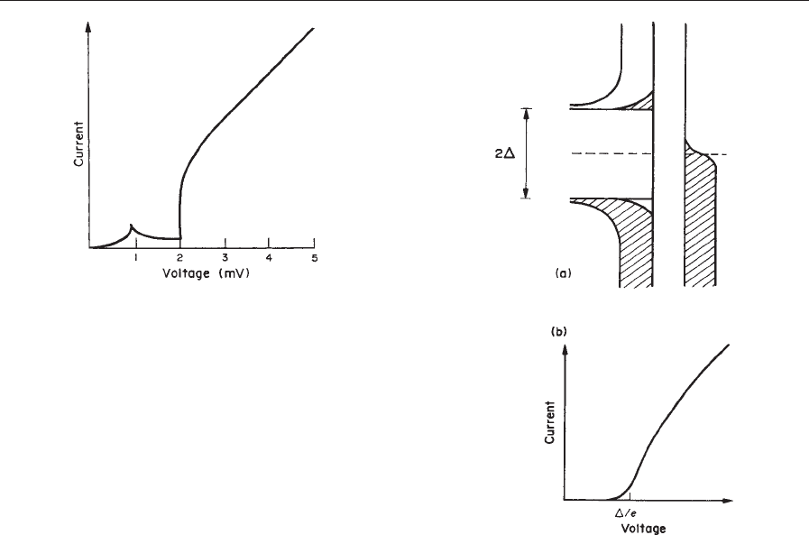
At high voltages, the current–voltage characteristic
approaches that of the normal state. The quasipar-
ticle branch of the characteristic is shown in Fig. 17;
the complete characteristic, including the Josephson
current of pairs flowing at V ¼0 exhibits the main
features of Fig. 8. Another interesting case is the S–I–
N junction, where N is a normal metal, for which the
density of states diagram and I–V characteristic are
shown in Fig. 18. The reader should be able to rec-
reate the I–V characteristics by following the process
of sliding the density of states as described.
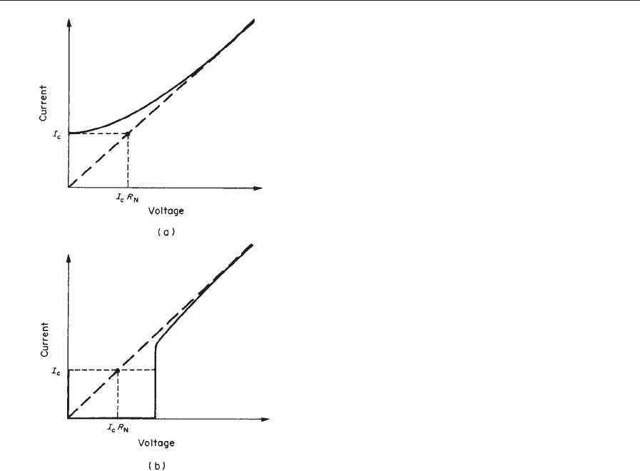
In weak link devices, as there is no tunnelling,
there is no signature of the energy gap in the I–V
characteristic. In many such devices, the I–V charac-
teristic resembles that for a tunnel junction with
a low-resistance shunt across it, the resistively
and capacitatively shunted junction (RCSJ) (see
Electrodynamics of Superconductors: Weakly Coupled ).
The I–V characteristic then appears as in Fig. 19.
An important ‘‘figure of merit’’ for both LTS and
HTS devices of both tunnelling and weak link types is
the I
C
R
N
product, which is the voltage defined in Fig.
19. It is related to the signal voltage that is available
in a SQUID or circuit. Obviously it should be large
(millivolts). It can be p3 mV in niobium tunnel junc-
tions, but in many HTS devices, especially the SNS
type, it is very small (e.g., tens of microvolts). This
makes such structures less interesting for practical
applications.
A second figure of merit, used for tunnel junctions,
is a measure of the subgap leakage current that flows
for voltages less than the energy gap compared with
the current that would flow at the same voltage in the
normal state. This can be expressed as the ratio R
S
/R
N
calculated at some defined voltage (e.g., 2 mV for nio-
bium devices), or as a voltage V
m
defined as R
S
times
the critical current I
c
. In an ideal junction, this current
is only due to quasiparticles that are thermally excited
above the gap. Hence, at temperatures small com-
pared with T
c
, it should be very small. For example,
for Pb–I–Pb junctions at 1 K values for R
S
/R
N
of 10
5
have been observed. For Nb–I–Nb at 4.2 K most of
the subgap current is thermally excited and the ratio is
about 20–25. Values lower than this indicate a poor
quality junction with some non-tunnelling leakage
paths for the excess current. The most obvious pos-
sibility is a small pinhole in the tunnel barrier.
4. Concluding Remarks
The discovery of the HTS oxides raises interesting
questions of how LTS and HTS junction technologies
will be used, assuming that the latter can be devel-
oped. There are strong signs that this will happen. In
some areas of application, it seems likely that HTS
and LTS technologies will compete with each other,
as they do with silicon and GaAs in some cases.
In one example, the most sensitive SQUIDs for
measuring magnetic signals from the brain might well
remain at 4.2 K, whereas for other measurements,
where portability of the equipment is needed (e.g.,
nondestructive evaluation of pipes) 77 K operation
will be favored.
The majority of the digital circuits that have been
built with niobium tunnel junctions employ ‘‘voltage
state logic,’’ in which the two states of the junction
are at zero voltage and about 2.9 mV. Power dissi-
pation is the product of the current and this voltage
for the time that the junction remains switched. If
HTS junctions of the same type could be made, the
advantages of the low power dissipation of super-
conducting technology would be partly lost. The
voltage (gap) would be ten times larger, and the cur-
rent also ten times larger (to scale with the operating
temperature); hence, the power would be 100 times
larger.
Figure 19
(a) The current–voltage characteristic for a weak link
with a resistively shunted junction RSJ type transition,
the I
C
R
N
product for the weak link is indicated; and (b)
I
C
R
N
product for Josephson tunnel junction.
1246
Thin Films, Multilayers and Devices, Supercondu cting

However, there is a class of superconducting cir-
cuits, known as QFP (quantum flux parametron) or
SFQ (single flux quantum) circuits, that avoid this
problem and, hence, regain the advantage of the very
low power dissipation of Josephson technology, even
at temperatures up to 77 K. The basic circuit element
is the SQUID and power is dissipated only when a
quantum of flux (which is the bit of information in
QFP) moves in or out of the SQUID loop. The mo-
mentary voltage pulse is the bit of information in
SFQ circuits. Such circuits do not need Josephson
junctions of the type shown in Fig. 8; in fact they can
use weak link devices. Thus, they appear to be the
most likely candidates for initial demonstrations of
HTS high-speed electronics.
Another divergence between LTS and HTS that is
already becoming apparent is the extensive use of fully
epitaxial multilayer devices in HTS. In this materials
aspect, HTS begins to resemble III–V semiconductor
technology much more than it does conventional su-
perconductor (niobium) technology. As an example,
an integrated HTS SQUID magnetometer has been
fabricated which utilized 15 epitaxial oxide layers of
superconductors and insulators, plus a final silver
contact layer (see Char et al. 1991a). Indeed, the field
of superconducting thin films, multilayers and devices
is changing and progressing rapidly.
See also: Films and Multilayers: Conventional
Superconducting; Metrology: Superconducting
Cryogenic Current Comparators; Superconducting
Machines: Energy Distribution Components; Super-
conduction Radiation Sensors; Superconducting
Thin Films: Materials, Preparation and Properties;
Superconducting Wires and Cables: Materials and
Processing
Bibliography
Anderson P W, Dayem A H 1964 Phys. Rev. Lett. 13, 195
Banerjee I, Yang Q S, Falco C M, Schuller I K 1983 Aniso-
tropic critical fields in superconducting superlattices. Phys.
Rev. B 28, 5037–40
Braginski A I, Talvacchio J 1990. In: Ruggiero S T, Rudman D
A (eds.) 1990 Superconducting Devices. Academic Press, San
Diego, CA, Chap. 8, p. 273
Brandt N B, Ginzburg N I 1960 Zh. Eksp. Teor. Fiz. 39, 1554
Buck D A 1956 Proc. IRE 44, 482
Buckel W, Gey W 1963 Z. Phys. 176, 336
Char K, Colclough M S, Garrison S M, Newman N,
Zaharchuk G 1991a Biepitaxial grain-boundary junctions in
YBa
2
Cu
3
O
7
. Appl. Phys. Lett. 59 , 733–5
Char K, Colclough M S, Lee L P, Zaharchuk G 1991b Exten-
sion of the biepitaxial Josephson junction process to various
substrates. Appl. Phys. Lett. 59, 2177–9
Eom C B, Sun J Z, Yamamoto K, Marshall A F, Luther K E,
Geballe T H, Cadermann S S 1989 In situ grown
YBa
2
Cu
3
O
7d
thin films from single-target magnetron sput-
tering. Appl. Phys. Lett. 55 (6), 595–7
Gao J, Aarnink W A M, Gerritsma G J, Veldhuis D, Rogalla H
1991 Preparation and properties of all high T
c
SNS-type edge
dc SQUIDS. IEEE Trans. Magn. 27, 3062–5
Geerk J, Gurvitch M, McWhan D B, Rowell J M 1982 Physica
109, 1775
Geerk J, Xi X X, Linker G 1988 Electron tunnelling into thin
films of Y
1
Ba
2
Cu
3
O
7
. Z. Phys. B 73, 329–36
Giaever I 1960 Phys. Rev. Lett. 5, 147
Greene L H, Bagley B G 1990 In: Ginsberg D M (ed.) 1990
Physical Properties of High Temperature Superconductors II.
World Scientific, Singapore, p. 509
Gross R, Chaudhari P, Dimos D, Gupta A, Koren G 1990a
Thermally activated phase slippage in higher T
c
grain bound-
ary Josephson junctions. Phys. Rev. Lett. 64, 228–31
Gross R, Chaudhari P, Kawasaki M, Ketchen M B, Gupta A
1990 Low noise YBa
2
Cu
3
O
7d
grain boundary junction dc
SQUIDS. Appl. Phys. Lett. 57, 727–9
Hammond R H 1975 IEEE Trans. Magn. 11, 201
Inam A, Hegde M S, Wu X D, Venkatesan T, England P, Miceli
P F, Chase E W, Chang C C, Tarascon J M, Wachtman J B
1988 As-deposited High-T
c
and J
c
superconducting thin films
made at low temperatures. Appl. Phys. Lett. 53, 908–9
Ivanov Z G, Nilsson P A, Winkler D, Brorsson G, Claeson T
1991 Proc. SQUID 1991 (in press)
Jia C L, Kabius B, Urban K, Herrman K, Cui G J, Schubert J,
Zander W, Braginski A I, Heiden C 1991 Microstructure of
epitaxial YBa
2
Cu
3
O
7
films on step edge SrTiO
3
substrates.
Physica C 175, 545–54
Josephson B D 1962 Phys. Lett. 1, 251
Karkut M G, Matijaservic V, Antognazza L, Triscone J-M,
Missert N, Beasley M R, Fischer Ø 1988 Anomalous upper
critical fields of superconducting multilayers—verification of
the Takahashi–Tachiki effect. Phys. Rev. Lett. 60, 1751–4
Kirk E C G, Blamire M G, Somekh R E, Evetts J E, Van
Vechten D, Lovellette M N 1991 Ultra-high quality Nb/
AlO
x
/Nb tunnel junctions with epitaxial base layers. IEEE
Trans. Magn. 27, 3137–40
Kleinsasser A W, Gallagher W J 1990 In: Ruggiero S T, Rud-
man D A (eds.) 1990 Superconducting Devices. Academic
Press, San Diego, CA, Chap. 9, p. 325
Li Y Q, Zhao J, Chern C S, Huang W, Kulesha G A, Lu P,
Gallois B, Norris P, Kear B, Cosandey F 1991 High critical
current densities in YBa
2
Cu
3
O
7x
thin films formed by met-
allorganic chemical vapor deposition at 730 1C. Appl. Phys.
Lett. 58, 648–50
Lowndes D H, Norton D P, Budai J D 1990 Superconductivity
in nonsymmetric epitaxial YBa
2
Cu
3
O
7x
/PrBa
3
Cu
3
O
7x
su-
perlattices—the superconducting behavior of Cu–O bilayers.
Phys. Rev. Lett. 65, 1160–3
Martens J S, Ginley D S, Beyer J B, Nordman J E, Hohen-
warter G K G 1991 A Josephson junction to FET high-speed
line driver made of T1CaBaCuO. IEEE Trans. Magn. 27,
3284–8
Rowell J M 1963 Phys. Rev. Lett. 11, 200
Ruggiero S T, Barbee T W, Beasley M R 1980 Phys. Rev. Lett.
45, 1299
Ruggiero S T, Barbee T W, Beasley M R 1982 Phys. Rev. B 26,
4894
Ruggiero S T, Rudman D A (eds.) 1990 Superconducting
Devices. Academic Press, San Diego, CA
Shinjo T, Takeda T 1987 Metallic Superlattices. Elsevier,
Amsterdam
Shoji A, Aoyagi M, Kosaka S, Shinokik F, Hayakawa H 1985
Niobium nitride Josephson tunnel junctions with magnesium
oxide barriers. Appl. Phys. Lett. 46, 1098–100
1247
Thin Films, Multilayers and Devices, Superconducting

Simon R 1991 High-T
c
thin films and electronic devices. Phys.
Today 44 (6), 64–70
Somekh R E, Shih W C, Dyrbye K, Huang K H, Baxter C S
1989 The Sputter Deposition of Metal Multilayers, X-Ray
Instrumentation, SPIE Vol. 1140. Society of Photo-Optical
Instrumentation Engineers, Bellingham, WA, pp. 453–63
Taber R C 1990 A parallel plate resonator technique for mi-
crowave loss measurements on superconductors. Rev. Sci.
Instrum. 61, 2200–6
Takahashi S, Tachiki M 1986 Theory of the upper critical
field of superconducting superlattices. Phys. Rev. B 33, 4620–
31
Van Duzer T, Turner C W 1981 Principles of Superconductive
Devices and Circuits. Elsevier, Amsterdam
J. M. Rowell
Conductus Inc., Sunnyvale, California, USA
Thin Films: Domain Formation
Soft magnetic films and nanostructures are of interest
for applications as sensors and storage material.
Most desirable are single-domain structures that
switch their magnetization at a certain field by fast
coherent rotation. These ideal films, so far, have not
been produced; the films tend to break up into do-
mains along the magnetization loop. The formation
of domains in soft magnetic films and nanostructures
has to be understood for the discussion of the mag-
netic properties of the films and nanostructures and
how to select them for applications.
A desirable ideal state of the magnetization in thin
ferromagnetic films is the single-domain state in
which at remanence the magnetization is directed
along an easy axis. Application of an external field
should cause coherent rotation of the magnetization
towards the applied field. Magnetization reversal is
expected by spontaneous switching at a critical field.
Nature does not follow these idealized assumptions.
For discussing the static equilibrium state of the
magnetization in a real sample one has to consider
the integral minimum of all magnetic energies: the
Zeeman energy e
H
¼
~
H
~
M of the sample in an ap-
plied field; the crystalline anisotropy energy e
K
; the
uniaxial anisotropy energy e
K
u
; the magnetostrictive
anisotropy energy e
s
; the exchange anisotropy e
ex
; the
external demagnetizing self-energy e
dext
¼(1/2)
~
H
dext
~
M, where
~
H
dext
is the demagnetizing field from
magnetic poles at the film boundaries; the intrinsic
demagnetizing self-energy e
dint
¼(1/2)
~
H
dint
~
M,
where
~
H
dint
is the demagnetizing field resulting from
intrinsic magnetization divergencies; the surface an-
isotropy s
s
; and the wall energy s
w
(Kittel 1949,
Craik and Tebble 1965).
All of these energy densities have to be integrated
over the volume of the film. Their minimum gives the
stable state of magnetization distribution in the
film. This problem is treated in the field of micro-
magnetism.
Experimental observation of domains gives a first
indication of how to approximate this difficult prob-
lem, which is then reduced to the domain theory,
in which the domains are separated by walls and
homogeneous magnetization is assumed within do-
mains (Kittel 1949).
The methods of domain observation have in-
creased in sensitivity and resolution over the years.
They include the Bitter pattern, magneto-optical Far-
aday and Kerr rotation, Lorentz microscopy, spin
polarized photoemission of electrons, and x-ray di-
chroism (Hubert and Scha
¨
fer 1998). These methods
will not be discussed in this article.
Why is the single-domain state of a film not a state
of lowest energy? Why does the film break up into
domains?
(i) The film size is finite. Magnetic poles at the
boundaries cannot be avoided in the single-domain
state, leading to strong magnetic self-energy. The to-
tal magnetic energy is decreased when this self-energy
is decreased by domain formation. The additional
increase in energy owing to domain wall energy is
smaller than the decrease of the self-energy.
(ii) Nonideal films, for instance polycrystalline
films, show fluctuation of the direction of the local
magnetization around the mean direction, the so-
called magnetization ripple (Hoffmann 1968). In
some cases this ripple is responsible for nucleation
of domains. The ripple prevents a coherent switching
of single domains.
Domain formation in thin films is many and var-
ied. It can be explained in the best way by discussing
soft magnetic thin films with uniaxial magnetic an-
isotropy, which are applied as magnetic sensors. The
uniaxial anisotropy results from film deposition in the
presence of a magnetic field parallel to the film plane
or from field annealing below the Curie temperature
of the deposited film. In both cases the direction of
the applied field introduces an easy axis of the mag-
netization parallel to the applied field. Permalloy
(Ni
91
Fe
19
) is the typical material used for soft mag-
netic uniaxial films.
1. The Single-domain Theory of Stoner and
Wohlfarth
The magnetization reversal of ideal uniaxial films is
theoretically described by the Stoner–Wohlfarth sin-
gle-domain theory (Stoner and Wohlfarth 1948,
Cohen 1969, Prutton 1964), in which an ideal uniax-
ial film with homogeneous in-plane magnetization is
assumed.
The in-plane magnetization loops with applied field
in the easy or hard direction are calculated from
the minimum of the Zeeman energy,
~
M
~
H, and the
1248
Thin Films: Domain Formation
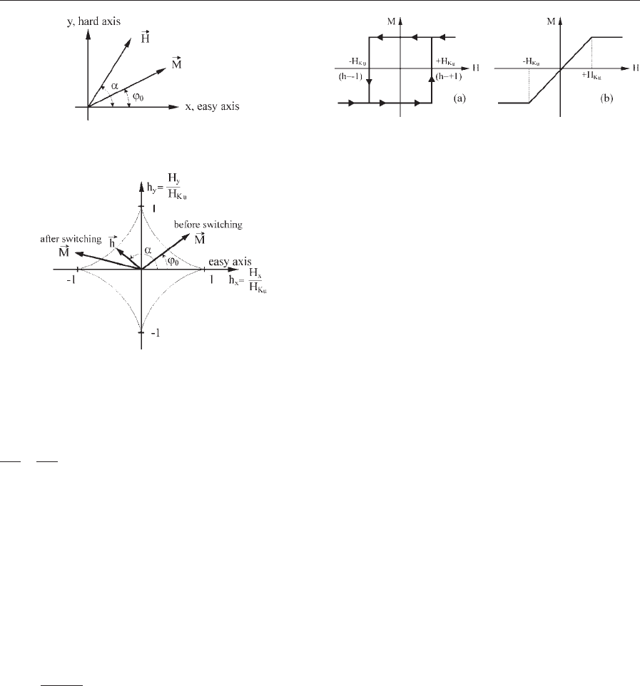
uniaxial anisotropy energy, K
u
sin
2
j
0
(Fig. 1), lead-
ing to
@e
@j
0
¼
@
@j
0
½HM cosða j
0
ÞþK
u
sin
2
j
0
¼HM sinða j
0
Þþ2K
u
sinj
0
cos j
0
¼ 0 ð1Þ
for the equilibrium state.
Introducing the anisotropy field H
K
u
¼2K
u
/M,
which is characteristic for uniaxial films, the equilib-
rium state is given by
h sinða2j
0
Þþcos j
0
sin j
0
¼ 0 ð2Þ
The field h ¼H/H
K
u
¼HM/2K
u
is the applied field
in units of H
K
u
, which will be used in the following
discussions.
The effective field, h(a), in units of H
K
u
, is given by
1
2K
u
@
2
e
@j
2
0
¼ hðaÞ¼h cosða j
0
Þþcos2j
0
ð3Þ
which determines the stability of the magnetization.
Stable states require h(a)40; instability, i.e. switch-
ing, occurs for h(a) ¼0 (Hoffmann 1966, 1968).
The equation
hðaÞ¼h cosða j
0
Þþcos2j
0
¼ 0 ð3aÞ
describes the well-known Stoner–Wohlfarth astroid
(Fig. 2) (Stoner and Wohlfarth 1948, Cohen 1969,
Prutton 1964).
On applying a field
~
H at an angle a to the easy axis,
for which the magnetization at H ¼0 was originally
saturated, the magnetization is coherently rotated by
an angle j
0
from the easy axis. As soon as the
applied field
~
H crosses the astroid, the magnetization
switches spontaneously by coherent rotation into a
new stable state (Fig. 2).
In the special case of applying the field along the
easy axis, the magnetization remains stable in the
original state, until at H ¼H
K
u
it switches spontane-
ously to the antiparallel direction by coherent rotation
(Fig. 3(a)). These two stable states, switched at H
K
u
,
make uniaxial films desirable for magnetic storage.
Unfortunately, in reality, coherent switching along the
easy axis is not observed. Instead, the magnetization of
the films breaks up into domains, and magnetization
reversal is completed by domain wall motion with co-
ercive force 7H
c
7o7H
K
u
7 (see Figs. 10(a) and (b)).
In the special case of applying the field along the
hard axis, the magnetization rotates continuously
from the easy axis against the direction of the applied
field, until at H ¼H
K
u
the magnetization is saturated
in this direction. The expected magnetization loop is
given in Fig. 3(b). In this way the uniaxial film is used
as a field sensor (see also Coercivity Mechanisms).
2. Magnetization Ripple
In discussing magnetization reversal in real polycrys-
talline films or in single-crystalline films, including
defects, one has to include inhomogeneous local an-
isotropies, such as crystalline anisotropy and magne-
tostriction of the crystallites. These local anisotropies
lead to deviations, j, of the local direction of the
magnetization from the mean direction j
0
. The mag-
netization is no longer homogeneous over the entire
film. The fluctuations are coupled in elliptical areas
over many crystallites. The major axis of the coupling
ellipse is always directed perpendicular to the mean
magnetization and is determined by dipolar coupling.
The minor axis, parallel to the mean magnetization, is
determined by the exchange length.
The fluctuation j can be seen in images obtained
by Lorentz microscopy (Fig. 4). This ‘‘magnetization
ripple’’ (Hoffmann 1966, 1968, Cohen 1969) dominates
Figure 2
Stoner–Wohlfarth astroid.
Figure 3
Magnetization loops of uniaxial films: (a) easy axis;
(b) hard axis.
Figure 1
System of coordinates and angles.
1249
Thin Film s: Domain Formation