Buschow K.H.J. (Ed.) Concise Encyclopedia of Magnetic and Superconducting Materials
Подождите немного. Документ загружается.

energy discrimination. The sampling depth of PEEM
correlates with the mean free path of low energy
electrons in the studied material and lies typically
between 2 nm and 5 nm for metals.
The emitted electrons are accelerated in the strong
electric field between the sample and the first micro-
scope lens (B10
4
Vmm
1
), and are then imaged with
magnification by electron optics, consisting of typi-
cally 2–4 electrostatic or magnetic lenses. A back fo-
cal plane aperture limits the angular spread of the
transmitted electrons and also acts as a simple energy
filter, reducing the chromatic and spherical aberra-
tions of the microscope. Projector lenses magnify and
focus the image onto the electron detector, typically
an electron sensitive phosphor and/or a channelplate
detector, producing a visible image. Deflector and
stigmator elements in the microscope steer the elec-
tron beam and correct for eventual mechanical
misalignments. Using synchrotron radiation micro-
scopes, has achieved a spatial resolution close to 20
nm (Anders et al. 1999).
2. Contrast Mechanisms
Contrast in PEEM results from local variations in the
light absorption, the work function, and the topog-
raphy of the sample. Topographic structures such as
edges, bulges, and holes locally distort the electric
field close to the sample and modulate the image in-
tensity. Work function contrast arises from inhomo-
geneities in the surface composition and thereby the
work function. This contrast mechanism is particu-
larly strong using UV radiation close to the work
function cut-off.
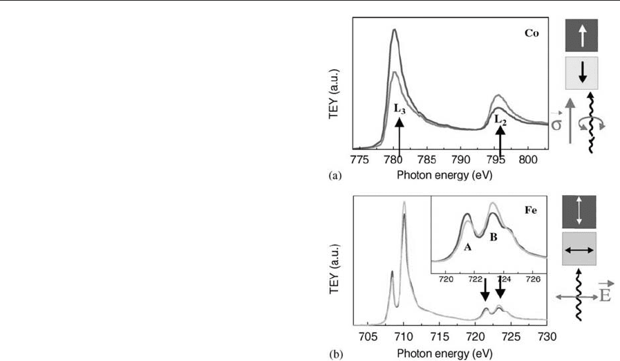
Chemical, magnetic, and elemental contrast arises
from Near Edge X-ray Absorption Fine Structure
(NEXAFS), which is discussed in more detail in Sur-
face Chemistry: Electron Yield Spectroscopy (Orme-
rod 2001). As an example, an x-ray absorption spec-
trum of a Co/FeMn/NiO multi-layer is shown in Fig.
2(b). Different elements in a material can be identified
by their characteristic core hole binding energies and
absorption edges. The fine structure close to the ab-
sorption edge—the inset shows the Ni L
2,3
edge—can
be further analyzed, providing information about the
chemical and magnetic state of the material. For ex-
ample, the multiplet structure at the L edges, marked
by arrows in Fig. 2(b), is characteristic for nickel
oxide (Regan et al. 2001).
PEEM microscopes are typically used in three
modes of operation: (i) full-field imaging, (ii) local
spectroscopy, and (iii) spectromicroscopy. In the full-
field imaging mode images are acquired at fixed pho-
ton energy. In the local spectroscopy mode local
x-ray absorption spectra are acquired in predefined
regions by scanning the photon energy and using the
spatial resolution provided by the PEEM electron
optics. In the spectromicroscopy mode, stacks of
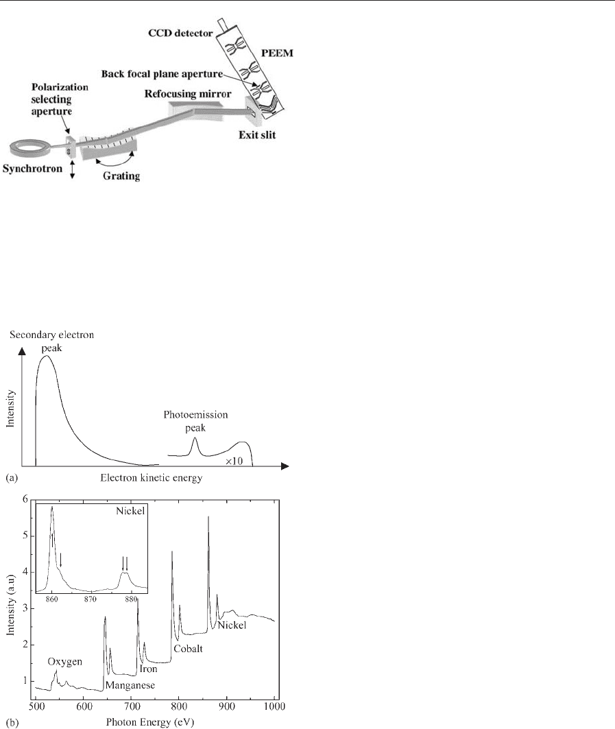
Figure 1
PEEM-2 Photoemission Electron Microscope and x-ray
beamline at the Advanced Light Source, USA. X rays
are monochromatized by a spherical grating and focused
into a 30 30 mm
2
spot on the sample. The electron
microscope column produces a magnified image of the
local x-ray absorption on a phosphor, which is imaged
by a slow-scan CCD camera.
Figure 2
(a) Energy spectrum of emitted electrons after the
absorption of x-rays. (b) X-ray absorption spectrum
measured in total electron yield of a Co/FeMn/NiO
sample. The absorption fine structure at the Ni L
2
peak
(inset) results from the presence of nickel oxide.
1230
Thin Film Magnetism: PEEM Studies
PEEM images are acquired as a function of photon
energy, generating a three-dimensional dataset with
two lateral and one energy dimension.
3. X-ray Magnetic Linear and Circular Dichroism
X-ray Magnetic Circular Dichroism (XMCD) and
X-ray Magnetic Linear Dichroism (XMLD) are es-
tablished spectroscopic x-ray techniques, which are
widely used for the investigation of ferromagnetic
and antiferromagnetic surfaces and thin films (Thole
et al. 1985, Schu
¨
tz et al. 1987, Alders et al. 1998, see
also Magnetism: Applications of Synchrotron Radia-
tion). Both methods probe the modification of the
electronic structure of a material in the presence of
magnetic order, resulting in an intensity variation of
the near edge x-ray absorption fine structure. X-ray
magnetic dichroism has been extensively used at 2p to
3d transitions (L
2,3
edge) in 3d transition metals, ex-
ploiting the strong spin–orbit interaction of 2p core
levels and the strong exchange splitting of 3d valence
levels (Schu
¨
tz et al. 1987). More recently XMLD has
been applied in studies of collinear antiferromagnets
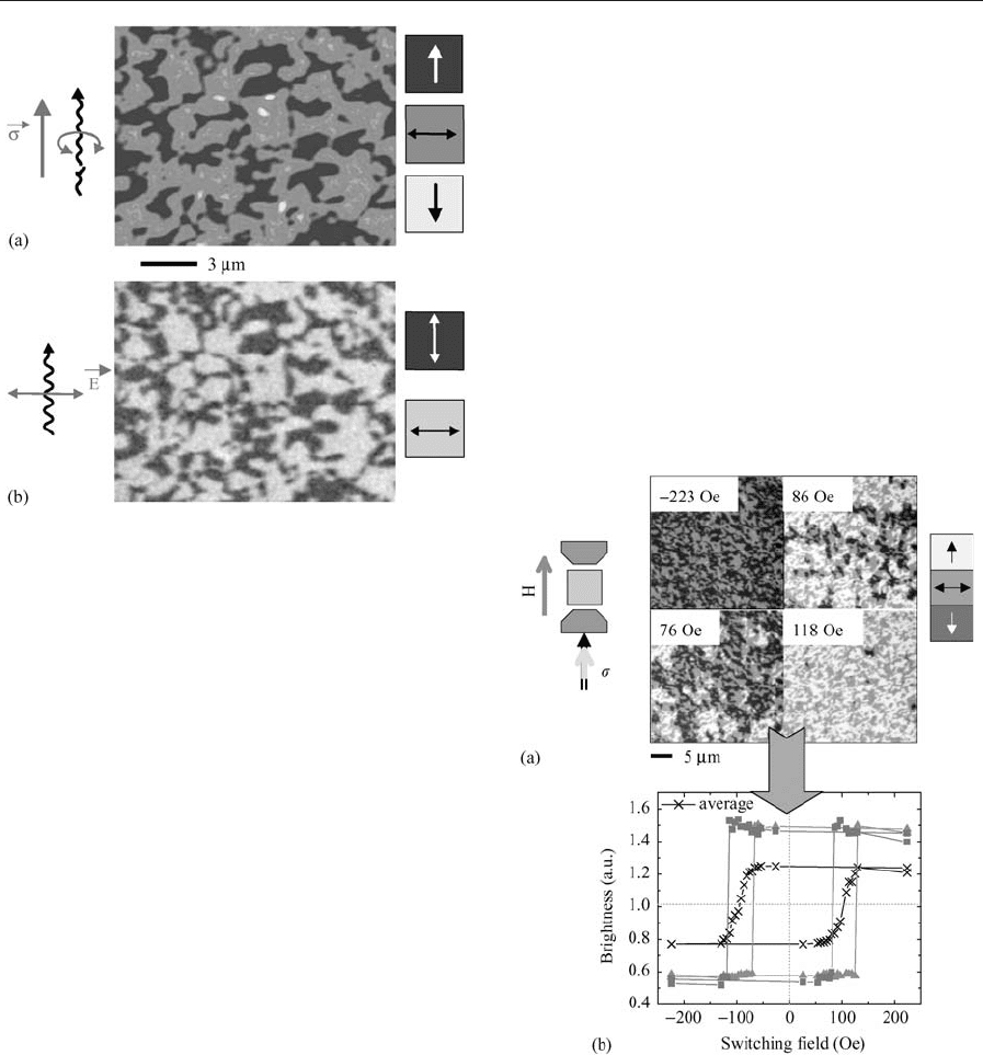
(e.g., Alders et al. 1998). In order to illustrate the
appearance of both dichroism effects, x-ray absorp-
tion spectra are shown in Fig. 3, measured in single
microscopic magnetic domains on a Co/LaFeO
3
bilayer.
The sample was grown by molecular beam epitaxy
(MBE) on a SrTiO
3
(001) substrate (Scholl et al. 2000).
The relative in-plane orientation of the photon polar-
ization and the sample magnetization are shown on
the right. The size of the XMCD effect in ferromag-
netic Co, which appears as a variation of the L
3
and
L
2
resonance intensities, depending on the relative
orientation of the sample magnetization M and the
circular x-ray polarization direction P, is a measure
for the element specific, atomic, spin, and orbital
moment and the angle enclosed by the magnetization
and the polarization vector: DIB M
jj
cos+ðM; PÞ
(Fig. 3(a)). Alternatively, XMLD is particularly use-
ful for the investigation of collinear antiferromagnet-
ism because it probes an anisotropic electronic
structure. Ideal antiferromagnets do not show XMCD
because they are magnetically compensated. The ab-
sorption spectrum of the antiferromagnetically or-
dered Fe atoms in LaFeO
3
shows a change in the
relative intensity of the L
3
and L
2
multiplet peaks due
to XMLD, depending on the relative orientation of
the LaFeO
3
magnetic axis and the linear x-ray polar-
ization (Fig. 3(b)). The size of the effect is again a
measure for the element specific, atomic, magnetic
moment M, and the angle enclosed by the spin axis A
and the linear polarization vector E: DIB M
2
½1 2cos
2
+ ðA; EÞ:
XMCD was first applied to ferromagnetic domain
imaging in a pioneering work in 1993 (Sto
¨
hr et al.
1993). More recently, microscopic antiferromagnetic
domains have been imaged for the first time using
XMLD (Scholl et al. 2000, Nolting et al. 2000). For
the study of ferromagnetic domains in transition
metal ferromagnets, e.g., Co, images are acquired
with the photon energy tuned to the peak of the L
3
and L
2
resonances. The ratio image acquired with
circular polarization is the XMCD image (Fig. 4(a)).
Alternatively, images acquired with opposite polari-
zation can be divided. Dividing PEEM images ac-
quired with linear polarization at the magnetically
sensitive peaks A and B at the L
2
edge of the anti-
ferromagnet LaFeO
3
generates the XMLD image,
representing the antiferromagnetic domain structure
of a material (Fig. 4(b)).
Different colors in the XMCD and XMLD image
correspond to different directions of the magnetic
moment. In Co (top) we distinguish three classes of
domains, which have magnetizations pointing up
(shown here as the darkest shade), down (lightest
shade), and left or right (medium shade, not distin-
guished in this measurement geometry). The XMLD
image of LaFeO
3
shows two classes of domains
with the in-plane projection of the atomic magnetic
Figure 3
(a) X-ray Magnetic Circular Dichroism (XMCD) and
(b) Linear Dichroism (XMLD) spectra of 1.2 nm Co/40
nm LaFeO
3
/SrTiO
3
(001). The LaFeO
3
spectrum was
acquired at the Fe edge. The spectra show opposite
dichroism effects (a) at the L
3
and L
2
resonance in the
ferromagnet Co (XMCD) and (b) at the L
2
multiplet
peaks A and B in the antiferromagnet LaFeO
3
(XMLD).
1231
Thin Film Magnetism: PEEM Studie s
moments pointing up down (darker shade) and left-
right (lighter shade). Note that the shown images
were acquired at identical sample positions, making
use of the element specificity of x-ray PEEM. The
correspondence between the two domain structures
indicates a uniaxial interface exchange coupling of
sufficient strength, aligning the magnetization in the
ferromagnet with the in-plane component of the
magnetic axis in the antiferromagnet.
4. Imaging of Local Exchange Bias
One important application of domain imaging using
the PEEM technique is the study of exchange biased
thin film systems. Exchange bias at a ferromagnet/
antiferromagnet interface leads to a unidirectional
anisotropy of the ferromagnetic layer, pinning its
magnetization into a preferred direction (Meiklejohn
and Bean 1956); see also Magnetic Films: Anisotropy.
This pinning is employed in magneto-electronic de-
vices for stabilization of the magnetization in a mag-
netic reference layer. The major application of this
effect is in magnetic hard disk heads containing a
read element based on the giant magnetoresistance
phenomenon (see Giant Magnetoresistance and Mag-
netic Recording Technologies: Overview). The unique
combination of elemental specificity, surface sensitiv-
ity, and ferro- and antiferromagnetic contrast of
PEEM allows studying the magnetic structure direct-
ly at the interface between two coupled layers, pro-
viding crucial insight into the microscopic coupling
mechanism (Ohldag et al. 2001). The unidirectional
pinning of the magnetization in a ferromagnet in
contact with an antiferromagnet can be made visible
by PEEM as shown in Fig. 5.
XMCD images of a ferromagnetic Co layer on La-
FeO
3
were acquired in remanence as function of the
applied magnetic field. Figure 5 shows a subset of a
field series, containing about 30 images. The strong
uniaxial interface coupling to the AFM prevents a
permanent rotation of the horizontally oriented mag-
netic domains (gray), which have a magnetization ori-
ented perpendicular to the field direction. Vertically
Figure 5
(a) Magnetization reversal of Co layer pinned by
LaFeO
3
underlayer. The images were acquired in
remanence after applying magnetic field pulses of
increasing strength. The correspondence of
magnetization direction to domain brightness is
illustrated on the right. (b) Local hysteresis loops were
calculated in single domains, showing exchange bias of
opposite sign (triangles/squares). The average loop
(crosses) was acquired by averaging the XMCD
intensity over the whole PEEM field of view.
Figure 4
X-ray magnetic dichroism images of (a) the
ferromagnetic domain structure in Co and (b) the
antiferromagnetic domain structure in LaFeO
3
in a
Co/LaFeO
3
/SrTiO
3
(001) multilayer sample. Different
shades refer to different domain orientations as
indicated in the boxes. The images demonstrate a
parallel orientation of the in-plane component of the Fe
and Co moment due to interfacial exchange coupling.
1232
Thin Film Magnetism: PEEM Studies

oriented domains, which have an easy axis along the
magnetic field, switch from black to white at about
100 Oe, indicating the reversal of the magnetization
parallel to the applied field. Remanent hysteresis loops
of two individual domains are shown at the bottom of
Fig. 5. The two representative loops show a relative
shift of the plus/minus and minus/plus switching fields
of about 50 Oe. This corresponds to a positive (neg-
ative) exchange bias field in the triangles (squares)
domain of þ25 (25) Oe. Averaging over a large
number of domains yields the average loop (black).
5. Conclusion
In comparison to other domain imaging techniques
x-ray PEEM stands out by its ability to separately
study the chemical, electronic, and magnetic proper-
ties of different materials in a layered or alloyed ma-
terial. The moderate surface sensitivity of the
technique permits the investigation of ultrathin mul-
tilayers but at the same time PEEM is sufficiently
sensitive to detect sub-monolayer amounts of mag-
netic moments. The spatial resolution of PEEM can
be further improved by aberration correction. Imple-
mentation of correction techniques promises an im-
provement of the spatial resolution close to the
physical limit of 1–2 nm. Another future application
of PEEM is the investigation of dynamical magnetic
processes, such as spin precession and magnetization
reversal, utilizing the pulsed structure of synchrotron
sources.
Bibliography
Alders D, Tjeng L H, Voogt F C, Hibma T, Sawatzky G A,
Chen C T, Vogel J, Sacchi M, Iacobucci S 1998 Temperature
and thickness dependence of magnetic moments in NiO epit-
axial films. Phys. Rev. B 57, 11623–31
Anders S, Padmore H A, Duarte R M, Renner T, Stammler Th,
Scholl A, Scheinfein M R, Sto
¨
hr J, Se
´
ve L, Sinkovic B 1999
Photoemission electron microscope for the study of magnetic
materials. Rev. Sci. Instrum. 70, 3973–81
Bauer E 1994 Low-energy electron microscopy. Rep. Prog.
Phys. 57, 895–938
Duden T, Bauer E 1998 Spin-polarized low-energy electron
microscopy. Sur. Rev. Lett. 5, 1213–9
Meiklejohn W H, Bean C P 1956 New magnetic anisotropy.
Phys. Rev. 102, 1413–4
Nolting F, Scholl A, Sto
¨
hr J, Seo J W, Fompeyrine J, Siegwart
H, Locquet J-P, Anders S, Lu
¨
ning J, Fullerton E E, Toney M
F, Scheinfein M R, Padmore H A 2000 Direct observation of
the alignment of ferromagnetic spins by antiferromagnetic
spins. Nature 405, 767–9
Ohldag H, Regan T J, Sto
¨
hr J, Scholl A, Nolting F, Lu
¨
ning J,
Stamm C, Anders S, White R L 2001 Spectroscopic identi-
fication and direct imaging of interfacial magnetic spins.
Phys. Rev. Lett. 87, 247201/1–4
Ormerod R M 2001 Surface Chemistry: Electron Yield
Spectroscopy. In Buschow K H J, Cahn R W, Flemings
M C, Ilschner B, Kramer E J, Mahajan S (eds.) Encyclopedia
of Materials: Science and Technology, Elsevier, Oxford, Vol.
9, pp. 9006–8
Regan T J, Ohldag H, Stamm C, Nolting F, Lu
¨
ning J, Sto
¨
hr J,
White R L 2001 Chemical effects at metal/oxide interfaces
studied by x-ray-absorption spectroscopy. Phys. Rev. B 64,
214422/1–11
Scholl A, Ohldag H, Nolting F, Sto
¨
hr J, Padmore H A 2002
X-ray photoemission electron microscopy, a tool for the in-
vestigation of complex magnetic structures. Rev. Sci. Instrum.
73, 1362–8
Scholl A, Sto
¨
hr J, Lu
¨
ning J, Seo J W, Fompeyrine J, Siegwart
H, Locquet J-P, Nolting F, Anders S, Fullerton E E,
Scheinfein M R, Padmore H A 2000 Observation of anti-
ferromagnetic domains in epitaxial thin films. Science 287,
1014–6
Schu
¨
tz G, Wagner W, Wilhelm W, Kienle P, Zeller R, Frahm
R, Materlik G 1987 Absorption of circularly polarized x rays
in iron. Phys. Rev. Lett. 58, 737–40
Sto
¨
hr J, Padmore H A, Anders S, Stammler T, Scheinfein M R
1998 Principles of x-ray magnetic dichroism spectromicro-
scopy. Surf. Rev. Lett. 5, 1297–308
Sto
¨
hr J, Wu Y, Hermsmeier B D, Samant M G, Harp G R,
Koranda S, Dunham D, Tonner B P 1993 Element specific
magnetic microscopy with circularly polarized x rays. Science
259, 658–61
Thole B T, Laan G, van der Sawatzky G A 1985 Strong mag-
netic dichroism predicted in the M
4,5
x-ray absorption spectra
of magnetic rare-earth materials. Phys. Rev. Lett. 55, 2086–8
Tonner B P, Dunham D, Droubay T, Kikuma J, Denlinger J,
Rotenberg E, Warwick A 1995 The development of electron
spectromicroscopy. J. Electron Spectrosc. Rel. Phenom. 75,
309–32
A. Scholl
Lawrence Berkeley National Laboratory, Berkeley
California, USA
Thin Films, Multilayers and Devices,
Superconducting
Thin films are an essential part of all electronic tech-
nologies. This is particularly true for superconducting
instrumentation, sensors and electronics, in which the
active devices themselves are made from deposited
films, often a sequence of films made as a multilayer
structure. This is in contrast to some semiconductor
technologies, in which devices are often created by
doping of bulk single crystals, say silicon or GaAs,
and are then linked together with interconnects and to
passive components (capacitors, resistors) that are
made from deposited films. In the most highly devel-
oped superconducting technology, namely Josephson
junction circuits operating at 4.2 K, the entire circuit
of junctions, resistors, capacitors, insulators and in-
terconnects is made from films that are deposited at
room temperature (a significant difference from semi-
conductor processing, which is carried out at high
temperatures). Thus, the control of thin-film processes
1233
Thin Films, Multilayers and Devices, Superconducting
is especially critical to the success of superconducting
electronics technologies. The important film synthesis
methods, the properties of superconducting films and
the devices made from them are the subjects of this
article, which therefore forms a link between articles
that are concerned predominantly with different ma-
terials or physical phenomena and articles that deal
with low-current applications.
The very significant differences between low-tem-
perature superconducting (LTS) materials and high-
temperature superconducting (HTS) materials have
already resulted in some divergence in the approaches
being used to make, understand and use LTS and
HTS films. In each section of this article LTS films
will be described first, then the differences in the HTS
cases will be identified. It is important to note that
LTS film studies and technology date from the late
1950s and are, hence, well established, whereas HTS
films are very recent and the field is subject to rapid
change.
1. Thin Films
1.1 Thin-film Synthesis
The various deposition methods that are available to
make thin films of all kinds can be readily used for
superconductors. These methods are thermal and
electron-beam evaporation and sputtering. Many el-
emental superconductors that have been used for
both science and applications studies (e.g., lead, tin,
indium, aluminum, zinc) can be made as films by the
simplest methods, which is thermal evaporation in a
moderate vacuum (10
4
Pa or 10
6
torr) onto a subst-
rate at room temperature. The nature of the substrate
is not critical, glass is quite adequate. Alloys of these
elements can be made by evaporation from two
sources or sometimes (e.g., PbBi) from a single
source.
Films of greater technological interest (e.g., nio-
bium, tantalum and their alloys with other transition
metals) are not easy to evaporate thermally, but elec-
tron-beam evaporation and sputtering are straight-
forward for such materials. Magnetron sputtering
sources have become the method of choice for the
niobium films used in Josephson circuits. Alloys can
be made from a sputtering target of the appropriate
composition. The superconducting properties of tran-
sition metals are more sensitive to impurities, such as
oxygen, than the s–p metals and a better vacuum
system must be used, say p10
6
Pa (10
8
torr). The
transition metals make excellent getters, so placing a
liquid-nitrogen-cooled surface near the substrate very
effectively lowers the system pressure. The substrate
temperature can be 300 K for niobium film deposi-
tion, but the resistance ratio of clean films made at
this temperature will be limited by the grain size.
Higher substrate temperatures are needed for some
transition metals (e.g., tantalum) and to increase the
grain size of niobium. In particular, high-quality
epitaxial films with long electronic mean free paths,
such as those used in SIS particle detectors, and epi-
taxial superlattices with mean free paths extending
over many layers (see later) are grown at tempera-
tures as high as 800 1C.
To form films of compounds based on niobium
which have higher critical temperatures, such as
NbN, NbCN and the family of A15 compounds
Nb
3
Sn, Nb
3
Ge, Nbj
3
Al (see Superconducting Materi-
als; Types of ) somewhat more complicated methods
are used. The nitrides and carbonitrides, which are
important materials for Josephson circuits operating
at 8–10 K, are made by sputtering niobium targets in
argon plus nitrogen or nitrogen plus methane onto
substrates at 100–1000 1C (Braginski and Talvacchio
1990). The A15 compounds have generally been
made by coevaporation from electron-beam sources,
say niobium and tin, but cosputtering from multiple
targets or sputtering from a single mixed target can
also be used. The geometry of the evaporation sourc-
es (see Fig. 1) creates a spread of compositions across
an array of substrates (Hammond 1975). This allows
measurements to explore the effects of stoichiometry
on the physical properties of the films. To form the
crystalline structure of the compound, a heated
substrate has to be used. Typical optimum temper-
atures are 880 1C for Nb
3
Sn, 900 1C for Nb
3
Ge.
These high deposition temperatures have limited the
interest in A15 compounds for electronics applica-
tions, although values over 700 1C are now accepted
as necessary for HTS films.
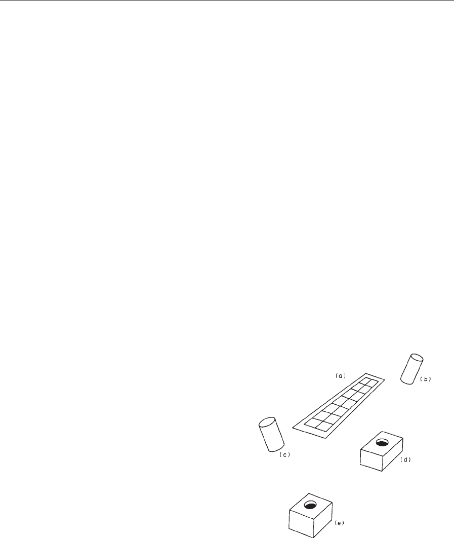
Figure 1
Arrangement of sources and substrates to achieve a
spread of compositions: (a) array of substrates heated to
800 1C; (b) niobium deposition-rate monitor; (c) tin
deposition-rate monitor; (d) niobium electron-beam
source; and (e) tin electron-beam source.
1234
Thin Films, Multilayers and Devices, Supercondu cting

To prepare films of the HTS materials, many of the
techniques described in this section are being used
(see High-temperature Superconductors: Thin Films
and Multilayers). The presence of three elements plus
oxygen in the HTS materials leads to increased com-
plexity of the deposition systems, particularly those
for cosputtering, sequential sputtering (a fraction of a
monolayer of each material is deposited sequentially
and repeated many times), coevaporation (MBE) and
sequential evaporation. Two comparatively simple
methods have quickly become popular and repro-
ducibly yield very-high-quality films. These are off-
axis sputtering (Eom et al. 1989) and laser ablation
(Inam et al. 1988). As in the case of A15 compounds,
HTS films are deposited at high temperatures (600–
750 1C) with the best films being made at X700 1C.
Unlike the transition metals, HTS films are deposited
in high oxygen pressures (sometimes 250 Pa) and,
hence, the base pressure of the vacuum system is less
relevant. One film process that is widespread for
semiconductors, chemical vapor deposition (Li et al.
1991), is being tried for HTSs with some success. It
has the potential to be a commercial process for films
of large area. At present typical film substrate sizes
are 4 in or 5 in diameter wafers for niobium circuits,
with plans in one laboratory to move to 8 in and 2 in
diameter for HTS devices.
A very significant difference between LTS and
HTS films is in the choice of substrates. Epitaxy be-
tween the substrate and film is essential for HTS
materials, hence, a very much more limited choice of
substrates is available. Because of the high deposition
temperatures, substrates for both HTS and A15 films
must not react chemically with the film at tempera-
tures up to around 800 1C. For most LTS films this is
not a consideration, but for those applications re-
quiring epitaxial films with long electronic mean free
paths, the substrate again must be chosen to have a
good lattice match and to be nonreactive.
1.2 Film characterization
Given the possibility that impurities introduced into
films during deposition will change their properties
from those exhibited by bulk samples of the same
material, characterization is an important part of
thin-film research. Important measurements include:
the resistivity of the film at 300 K, which will be in-
creased by impurities and disorder; the resistivity ra-
tio between 300 K and (say) 10 K, which is strongly
reduced by impurities and electron scattering from
the film surfaces; the transition temperature T
c
, which
is generally decreased by impurities but can some-
times be increased by disorder; the critical current
density J
c
, which can be most easily measured by
making a constriction in the film; the stoichiometry,
which can be determined by Rutherford backscatter-
ing, inductively coupled plasma spectroscopy or en-
ergy/wavelength dispersive x-ray analysis; and the
crystalline perfection, which is studied by x-ray scat-
tering or channelling techniques.
Of these characterization techniques, one of the
simplest and most informative is the measurement of
resistivity and resistivity ratio ðr
300K
=r
10K
Þ. For ex-
ample, r
300K
C15 mO cm for niobium implies an elec-
tronic mean free path of 3 nm. As phonon scattering
is reduced with decreasing temperature, scattering
from grain boundaries and lattice defects (or the film
surface) becomes dominant, for films deposited in a
poor vacuum system scattering by included impuri-
ties becomes important. Thus, a resistivity ratio of 7
implies a mean free path at 10 K of 21 nm, whereas 50
implies 150 nm. The ratios of 7 and 50 are typical of
niobium films made on room-temperature and heated
substrates. If the film thicknesses are larger than the
mean free path, the resistivity ratio is an immediate
indicator of film quality. In some epitaxial niobium
films, resistivity ratios as large as 300–400 in 2 mm
thick films have been reported. For many materials
(e.g., silver, niobium, molybdenum, tin, gallium) pre-
cision deposition techniques enable films to be de-
posited with mean free paths that are so long at low
temperatures that the resistance ratio is generally
limited by surface scattering, unless the films become
very thick.
These measurements are commonly used for both
LTS and HTS superconducting films. In the HTS
case, an important additional parameter of interest is
the surface impedance R
s
at frequencies in the range
from 1 GHz to 100 GHz. The importance of micro-
wave applications of HTS films has created the need
to measure R
s
from 4.2 K to at least 77 K (see
Superconducting Microwave Applications: Filters). As
R
s
for good HTS films is at least an order of mag-
nitude below that of copper, a copper cavity cannot
be used for the measurements at 77 K. A niobium
cavity can be used at 4.2 K. No standard measure-
ment method exists, but a technique which deter-
mines the Q of a resonator made of two HTS films
facing each other is becoming popular (Taber 1990).
1.3 Physical Properties of Films
Many of the properties of superconducting films are
discussed in other articles, in that they are identical to
those of the bulk material. However, thin films are
often used in preference to single crystals or poly-
crystalline samples, for three reasons. First, they al-
low certain experiments to be carried out more easily.
Examples are high-frequency properties, where a film
can be prepared with a smooth clean surface more
easily than the bulk; nonequilibrium properties,
where the sample volume can be made small; Jose-
phson effects in weak links (see Electrodynamics of
Superconductors: Weakly Coupled ), which are most
easily defined in films; tunnelling spectroscopy for
1235
Thin Films, Multilayers and Devices, Superconducting

which tunnel junctions are prepared by oxidizing
clean film surfaces; and proximity effect studies,
in that films can easily be made with thickness
comparable to a coherence length (at least in LTS
materials).
The second reason for using films for scientific
studies is that they can be made to exhibit properties
that are different from those of the same bulk ma-
terial. These differences can arise because of dimen-
sional effects, as films can be grown very thin in the
dimension normal to the substrate and can be pat-
terned to be small in the plane. When the thickness of
the film is less than the coherence length, it becomes
two dimensional, in that its properties cannot vary in
the direction normal to its surfaces. These dimen-
sional (including dimensional crossover effects) ef-
fects will be discussed in Sect. 2.
Another difference between film and bulk materials
can be created because the structure and electronic
properties of the film are changed by the deposition
process. This is generally a result of crystalline dis-
order (see Superconducting Materials: Irradiation
Effects). If the film is deposited on a substrate that
is too cold to allow ordering to occur, a very-small-
grained or even amorphous film can result (see Amor-
phous Superconductors). An early example was the
nonsuperconducting semimetal bismuth, which be-
came superconducting up to 6 K when deposited on a
substrate held at 4.2 K. The T
c
of gallium is similarly
raised from 1.1 K to 8.5 K by such ‘‘quench conden-
sation.’’ Such films were the first amorphous metals
(Brandt and Ginzburg 1960, Buckel Gey 1963). Al-
uminum films can have a T
c
up to 6 K compared to
the bulk 1.2 K, the T
c
depending largely on the con-
ditions of deposition and the strain induced by the
substrate. Such changes in T
c
are due to modification
of both the phonon spectrum and the density of elec-
tronic states of the material. In crystalline transition
metals, with their well known dependence of T
c
on
electron-to-atom ratio (see Superconducting Materi-
als: Types of ), a remarkably different dependence is
observed when films are deposited at low tempera-
tures to make them amorphous. Such quench-con-
densed films have high resistivities and small
resistance ratios (close to 1).
A third reason for using films is for superconduct-
ing applications in devices and electronics, as de-
scribed later in this article and in other more specific
contributions on particular application areas.
The same reasons for interest in the physical prop-
erties of LTS films apply to HTS materials. However,
the radically different properties of the HTS oxides
do create some different results. For example, the
oxides have anisotropic and very short coherence
lengths. Most HTS films are grown with the c-axis
normal to the substrate, with the copper oxide sheets
in the plane of the substrate. The c-axis coherence
length is only a few tenths of nanometers. Thus, the
surfaces of HTS films, unlike their LTS counterparts,
are most unlikely to have properties representative of
the bulk material (even those properties along the c
axis). This is because any change in stoichiometry, for
example loss of oxygen, or disorder, including that
due to surface reconstruction of the lattice, can affect
a surface layer whose thickness is comparable to, or
greater than, a coherence length. Thus, any experi-
ments that are surface sensitive, such as tunnelling,
proximity effects and photoemission studies, are un-
likely to measure bulk properties of HTS materials in
measurents on c-axis films. Recently, films with other
orientations have been deposited (see High-tempera-
ture Superconductors: Thin Films and Multilayers);
measurements on these films are likely to reveal more
of the bulk properties of HTS materials. In LTS ma-
terials the coherence length is generally much longer
than the thickness of any surface layer, although
niobium and A15 films can exhibit problems of sur-
face degradation unless care is taken.
Effects of dimensionality are also different in HTS
materials, in that even in the bulk they are strongly
anisotropic and can be considered pseudo two di-
mensional. It is also not possible to produce films
thinner than the coherence length along the c axis.
The coherence length is only 4 nm in the a–b plane of
YBCO, so even a-axis films are difficult to make thin
compared to this length. The effect on physical prop-
erties of making the films thin is most easily studied
in superlattices (see Sect. 2) but remarkably thin HTS
films have been made that remain superconducting to
quite high temperatures.
The properties of both films and bulk HTS mate-
rials can differ significantly from optimum values,
particularly due to loss of oxygen, to crystalline dis-
order and to doping effects. The trend of these effects
is to decrease T
c
and increase resistivity until the
material becomes insulating at low temperatures
(Greene and Bagley 1990).
There is one parameter that is very different in
films compared to bulk single crystals, especially in
the case of YBCO. This is the value of critical current
J
c
. All good HTS films with T
c
close to 90 K, inde-
pendent of their method of preparation, have J
c
val-
ues at all temperatures oT
c
much higher than those
for single crystals. It appears that a pinning center is
rather readily produced in thin films that is difficult
to reproduce in crystals and that this defect is com-
mon to all ‘‘high quality’’ YBCO films to date.
2. Superlattices
As an object of scientific study, multilayers or super-
lattices are an interesting class of ‘‘engineered’’ ma-
terials in the fields of semiconductors, magnetism (see
Thin Film Magnetism: PEEM Studies), optics, x-ray
optics and superconductivity (Shinjo and Takeda
1987). They are made by sequentially depositing two
or more materials many times (e.g., ABABABy).
1236
Thin Films, Multilayers and Devices, Supercondu cting
The individual film thicknesses of A and B approach
one atomic layer in some cases. This repetition of the
film sequence distinguishes them from the multilayer
device structures to be discussed later.
In semiconductors the long electron wavelength
(B10 nm) implies that the bulk electronic band struc-
ture can be radically changed in the direction normal
to the layers of a superlattice, once the individual
layers have thickness comparable to this wavelength.
This regime is relatively straightforward to reach with
current growth capabilities such as MBE. Thus, semi-
conductor superlattices have become a field of intense
activity, for both their research interest and device
potential. In metals, the short electron wavelength
(a few tenths of nanometers) implies that such band
structure changes cannot be observed. When metals
become superconducting, however, the electron wave-
length is replaced by the coherence length as the im-
portant length parameter. In LTS materials, it is easy
to make superlattices with layer thickness much less
than coherence lengths (typically tens of nanometers).
Hence, there is scientific interest in superconducting
superlattices, in which the components A and B can
be superconductor (A) with another superconductor,
metal, semiconductor or insulator (B).
It is important to note that in HTS superlattices, at
least those with c axis normal to the substrate, it is
again not possible to make the layer thickness thinner
than the coherence length, which is only a few tenths
of nanometers. If the HTS materials were strictly two
dimensional, layering them into a superlattice should
have no effect on T
c
unless structural effects occurred
(see later).
Unlike semiconductor superlattices, at present
there are no important devices made from supercon-
ducting superlattices (in contrast to multilayer device
structures), although the Nb/Al–Al oxide–Nb trilayer
process that is now the metallization of choice for
Josephson circuits was a direct result of studies of
tunnelling in niobium–aluminum superlattices (Geerk
et al. 1982).
2.1 Superlattice Synthesis
The vacuum equipment that is commercially availa-
ble makes it relatively easy to prepare superconduct-
ing superlattices. A substrate is exposed to alternating
sources of materials, for example by moving shutters
in front of electron-beam sources, or by rotating or
oscillating the substrate in front of two sputtering
sources. Magnetron sputtering sources are particu-
larly suitable because of the stability of their depo-
sition rate. It is often important to heat the substrate,
as the resulting films (e.g., niobium, tantalum) will
then have larger grain size, longer electron mean free
path and longer coherence lengths. Superlattices of
HTS materials have been made by the same methods.
Obviously a heated substrate (B700 1C) is always
necessary. In addition, laser deposition lends itself
ideally to the synthesis of HTS superlattices. Two
targets are moved alternately into the focus of the
laser beam and the layer thickness is controlled by the
number of laser shots allowed to impinge on each
target (Lowndes et al. 1990).
2.2 Superlattice Characterization
As a superlattice has an additional periodicity of the
structure in the growth direction, which is superim-
posed on the crystal lattice spacing, an important
measurement is the standard y–2y x-ray scan. An ex-
ample is shown in Fig. 2, where the subsidiary maxi-
ma are due to x-ray reflections from the superlattice
(Somekh et al. 1989). The position of these maxima
can be used to determine the superlattice wavelength
(the sum of the A and B layer thicknesses) and their
intensities are related to the interfacial roughness be-
tween layers.
Another important measurement is simply the net
resistivity of the superlattice (in the case of two met-
als). If the electron mean free path is long, that is, the
electrons move freely through the interfaces between
A and B, then the resistivity will have a value between
the values of A and B in their bulk form. However, if
the electrons are scattered at the interfaces, or if the
films themselves become structurally disordered due
to the layering process or to strain, then the resistivity
will be higher than the values of A or B. Even in
superlattices of superconductors with other materials
(insulators, semiconductors), or in HTS superlattices,
the resistivity and resistance ratio are very important
parameters to measure.
Transmission electron microscopy can yield ele-
gant pictures of superlattices and can be used to give
the orientation of the individual layers or grains
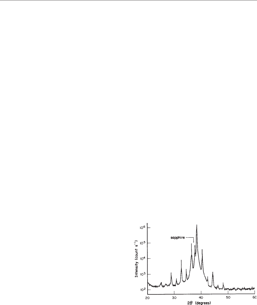
Figure 2
CuK alpha x-ray trace of niobium–tantalum epitaxial
multilayer (4.9 nm wavelength) grown on A-plane
sapphire to give (110) niobium–tantalum epitaxy; from
the superlattice intensities the interface roughness can be
estimated at 0.22 nm (after Somekh et al. 1989).
1237
Thin Films, Multilayers and Devices, Superconducting
within the layers. In the HTS materials, the layered
nature of the oxide structure gives even more striking
results. One example shows that within the one layer
there is a very abrupt change from YBCO to PrBCO,
presumably the result of ledge growth of the layers of
unit cell dimensions, that is, the layer was growing as
one unit cell of YBCO say when the source was
changed to PrBCO, which continued the growth to
complete the layer. This ledge growth is also clearly
evident in scanning tunnelling microscope profiles of
the surface of YBCO films (not superlattices), in
which the layers of one unit cell in height are shown
around screw growth dislocations.
2.3 Physical Properties of Superlattices
The superconducting property of LTS superlattices
that has received by far the greatest attention is the
upper critical field H
c2
, measured with the field ap-
plied parallel to the layers. This is because the di-
mensionality of the superconducting state is readily
determined from the form of the dependence of H
c2
on temperature T.
As an example, consider the specific case of a su-
perlattice of niobium–germanium (germanium films
are insulators at low temperatures) (Ruggiero et al.
1982). If the niobium layers are thick (tbx), then the
superlattice behaves like bulk niobium, that is, it is
three dimensional. If the niobium layers are thin (t5x),
and the germanium is thick, then the niobium layers
are isolated from each other and are two dimensional.
However, if the niobium layers are again, thin, and the
germanium layers are thin enough to allow appreciable
coupling by tunnelling between the niobium layers,
then bulk three-dimensional behavior is again recov-
ered, as the superlattice appears again as uniform ma-
terial over the length scale of x. Interesting crossover
effects have been observed as a function of tempera-
ture, in that the coherence length is much longer near
T
c
than it is at lower temperatures. Hence, it is possible
to find two regimes, one at higher temperatures where
x4t and three-dimensional behavior is observed and
another at low temperatures with xot that exhibits
two-dimensional behavior. As these two regimes have
different temperature dependences of H
c2
,namely
H
c2
CT
c
T for three dimensions and H
c2
C(T
c
T)
1/2
for two dimensions, the crossover between them is ob-
served in the plot of H
c2
vs T (see Fig. 3). These re-
gimes can be thought of as the situations where the
cores of the flux vortices either extend across multiple
layers as Abrikosov vortices (three dimensional) or sit
between the niobium layers in the germanium layers as
Josephson vortices (two dimensional).
A second type of superlattice utilizes superconduct-
ing and normal metals (e.g., SNSNSNy). The cou-
pling between the S layers is by the proximity effect
induced in the N layer. A widely studied example is
niobium–copper superlattices, in which one unusual
effect occurs for small periods (t2 nm). Both the
niobium and copper layers appear to become disor-
dered, with a strong increase in resistivity, a decrease
in resistance ratio and decrease in the T
c
of the nio-
bium. Dimensional crossover effects can also be ob-
served in SN superlattices as the N layer becomes
longer than its effective coherence length, which in
copper in niobium–copper superlattices was demon-
strated to be about 20 nm (Banerjee et al. 1983).
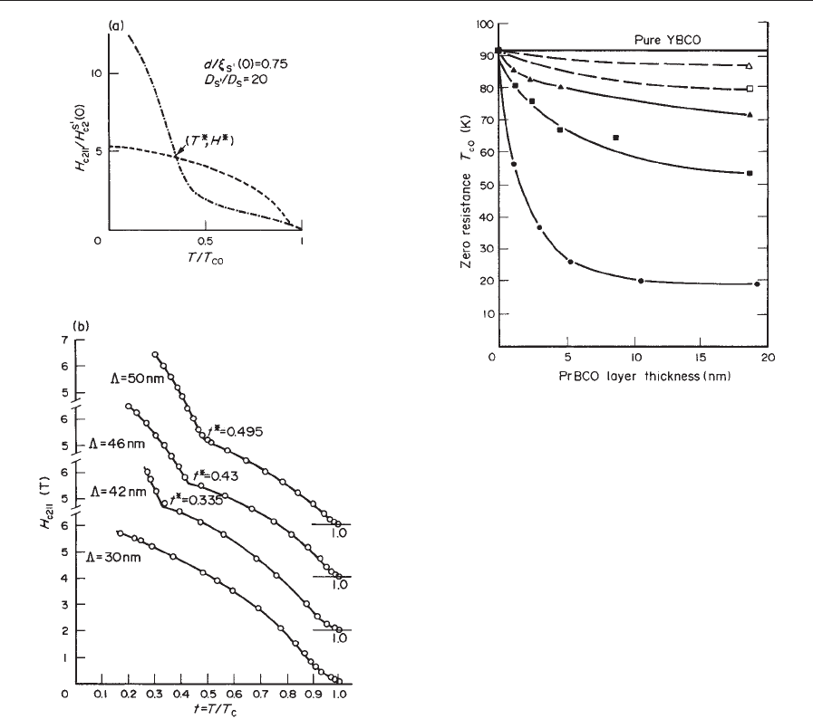
More recently, a further novel transition was pre-
dicted (Takahashi and Tachiki 1986) and observed
(Karkut et al. 1988) in superlattices of two super-
conductors with very similar T
c
but with very differ-
ent mean free paths, for example, niobium and a
niobium–titanium alloy. In this case two crossover
transitions were observed. Near T
c
the vortices are
located in the niobium–titanium but are large enough
to extend across the niobium (three dimensional,
H
c
C(T
c
T)). At a lower temperature x
Nb
becomes
less that t
Nb
and the vortices relocate into the nio-
bium layers and are confined within them (two di-
mensional, H
c2
C(T
c
T
1/2
)) (see Fig. 4). At even
lower temperatures, x
NbTi
becomes ot
NbTi
and the
vortices become two dimensional within the nio-
bium–titanium layers, which have a very high H
c2
.
Work on HTS superlattices is naturally at an ear-
lier stage, although the layered nature of the oxide
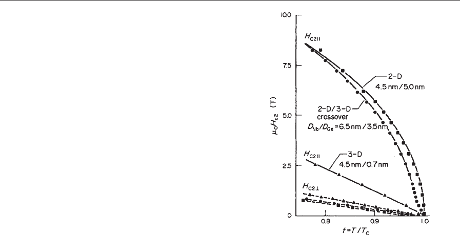
Figure 3
Upper critical fields near T
c
for Nb–Ge multilayers.
Systematically varying the germanium thickness
between the two-dimensional niobium layers effects a
progression from anisotropic three-dimensional
behavior ½H
c28
ðTÞBðT
c
TÞ to ‘‘crossover’’ behavior
and finally to decoupled two-dimensional behavior
½H
c28
ðTÞBðT
c
TÞ
1=2
(after Ruggiero et al. 1980).
1238
Thin Films, Multilayers and Devices, Supercondu cting
materials has allowed superlattices of very impressive
perfection to be grown. Perhaps the most interesting
question to be answered to date is the value of T
c
as
the individual HTS layers are made thinner and as
the coupling across an intermediate layer is made
weaker. The intermediate layer is, for example,
PrBCO which is a lattice-matched oxide that is a
Mott insulator that exhibits high electrical resistivity
at low temperatures. The results of Fig. 5 show that
even layers of YBCO that are one unit cell thick have
a T
c
of 20 K when widely separated (Lowndes et al.
1990). The T
c
increases as the coupling increases,
reaching 56 K when the PrBCO is one unit cell thick.
It is evident that HTS materials with a pronounced
perovskite layer structure behave in many respects
as intrinsic atomic-scale multilayers, the alternating
layers being the copper oxide planes (S) and the redox
spacer layers (N or I) (see Superconducting Materials:
Types of ). In the more complex HTS materials
the doping levels on the two types of layer may be
varied independently, their character changing from
ySNSNSNy to ySISISISy depending on the
preparation conditions. The interpretation and mod-
elling of HTS materials as intrinsic multilayer struc-
tures is currently an active area of considerable
importance both for their basic physical properties
and for their behavior in magnetic fields.
3. Superconducting Device Structures
Superconducting devices are rather simple structures
compared to those that are commonplace in semi-
conductor technology. This perhaps reflects the orders
Figure 4
(a) Theoretical temperature dependence of the parallel
critical fields for a multilayer SS
0
SS
0
SS
0
y . The dashed
and dash-dotted curves indicate the upper critical fields
when the superconducting order parameter nucleates in
the S and S
0
layers respectively. The observable H
c28
is
the higher one of the two critical fields at each
temperature. The point (T
*
, H
*
) is a multicritical
crossover point, d is the layer thickness and D is the
diffusivity (after Takahashi and Tachiki 1986). (b)
Resistive measurements of H
c28
vs tð¼ T=T
c
Þ for
Nb/NbTi superlattices with layers of equal thickness
showing behavior at t
*
for samples with different
wavelength L (after Karkut et al. 1988).
Figure 5
Critical temperature of (YBCO)
M
/(PrBCO)
N
superconducting multilayers (m ¼1 to 8 unit cells thick)
vs the separating PrBCO layer thickness: D, eight-cell
YBCO; &, four-cell YBCO; m, three-cell YBCO; ’,
two-cell YBCO; *, single-cell YBCO (after Lowndes
et al. 1990).
1239
Thin Films, Multilayers and Devices, Superconducting