Bhushan B. Nanotribology and Nanomechanics: An Introduction
Подождите немного. Документ загружается.

13 Computer Simulations of Nanometer-Scale Indentation and Friction 667
F
z
(nN)
0
60
20
40
M
L
Q
S
U
W
X
V
T
R
D
O
P
N
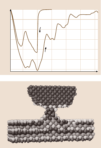
Fig. 13.3. Computationally
derived force F
z
versus tip-
to-sample distance d
hs
curves
for approach, contact, inden-
tation, then separation using
the same tip–sample system
shown in Fig. 13.4. These
data were calculated from an
MD simulation. After [111]
with the permission of the
AAAS (1990)
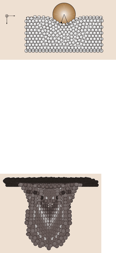
Fig. 13.4. Illustration of
atoms in the MD simulat-
ion of a Ni tip being pulled
back from an Au substrate.
This causes the formation of
a connective neck of atoms
between the tip and the sur-
face. After [111] with the
permission of the AAAS
(1990)
occurs increases, as does the contact area between the tip and the surface and the
amount of nanowire elongation prior to breakage.
Simulations by Komvopoulos and Yan [122] using LJ potentials showed how
metallic surfaces respond to single and repeated indentation by metallic, or cova-
lently bound, rigid tips. The simulations predicted that a single indentation event
produces hysteresis in the force curve as a result of surface plastic deformation
and heating. The repulsive force decreases abruptly during surface penetration by
the tip and surface plastic deformation. Repeated indentation results in the continu-
ous decrease of the elastic stiffness, surface heating, and mean contact pressures at
maximum penetration depths to produce behaviors that are similar to cyclic work
hardening and softening by annealing observed in metals at the macroscale.
When the tip is much stiffer than the surface,pile-up of surface atoms aroundthe
tip occurs to relieve the stresses induced by nanoindentation. In contrast, when the
surface is much stiffer than the tip, the tip can be damaged or destroyed. Simulat-
ions by Belak et al. [123] using perfectly rigid tips showed the mechanism by which
the surface yields plastically after its elastic threshold is exceeded. The simulations
showed how nanoindentation causes surface atoms to move on to the surface but
668 Susan B. Sinnott et al.
under the tip and thus cause atomic pile-up. In this study, variations in the inden-
tation rate reveal that point defects created as a result of nanoindentation relax by
moving through the surface if the rate of indentation is slow enough. If the indenta-
tion rate is too high, there is no time for the point defects to relax and move away
from the indentation area and so strain builds up more rapidly. The rigid indenters
considered in these MD simulations are analogous to experiments that use surface
passivation to prevent JC between the tip and the surface [120,124], the results of
which agree with the predicted results of pile-up and crater formation, as shown in
Fig. 13.5 [120].
In short, MD simulations are able to explain the atomic-scale mechanisms be-
hind measured experimentalforce curves producedwhen metal tips indent homoge-
neousmetal surfacesto nanometer-scaledepths. Thispreliminary workhas spawned
much of the current interest in using the JC to produce metal nanowires [126–128].
MD simulations have also been used to examine the relationship between
nanoindentation and surface structure. This is most apparent in a series of com-
putational studies that consider the indentation of a surface with a “virtual” hard-
sphere indenter in a manner that is independent of the rate of indentation, as shown
in Fig. 13.6. The virtual indenter is modeled through the application of a repulsive
force to the surface rather than through the presence of an actual atomic tip. Kelch-
ner et al. [129], rather than use MD, pushed the indenter against the surface a short
distance and then allowed the system to relax using standard energy minimization
methods in combination with EAM potentials. The system is fully relaxed when the
energy of the surface system is minimized. After relaxation,the tip is pushed further
into the surface and the process is repeated. As the tip generates more stresses in the
surface,dislocationsare generated andplastic deformationoccurs. If thetip is pulled
back after indenting less than a specific critical value, the atoms that were plastically
deformed are healed during the retraction and the surface recoversits original struc-
ture. In contrast, if the tip is indented past the critical depth, additional dislocations
1ìm
100nm
Z
Before
1ìm
1ìm
100nm
Z
After
1ìm
Fig. 13.5. Images of a gold surface before and after being indented with a pyramidal shaped
diamond tip in air. The indentation created a surface crater. Note the pile-up around the crater
edges. After [120] with the permission of Elsevier (1993)
13 Computer Simulations of Nanometer-Scale Indentation and Friction 669
Free surface
Fixed
B.C.
Fixed
B.C.
Fixed B.C.
x
y
z
Free surface
r
i
R
Indenter
Fig. 13.6. A schematic of a spherical, virtual tip indenting a metal surface. After [125] with
the permission of Elsevier (1993)
are created that interfere with the surface healing process on tip withdrawal. In this
case, a surface crater is left on the surface following nanoindentation.
A similar study by Lilleodden et al. [125] considered the generation of disloca-
tions in perfect crystals and near grain boundaries in gold. Analysis of the relation-
ship between the load and the tip displacement in the perfect crystal shows discrete
load drops followed by elastic behavior. These load drops are shown to correspond
to the homogeneous nucleation of dislocations, as illustrated in Fig. 13.7, which
is a snapshot taken just after the load drop. When nanoindentation occurs close to
a grain boundary, similar relationships between the load and tip displacement are
predicted to occur as were seen for the perfect crystal. However, the dislocations
responsible for the load drop are preferentially emitted from the grain boundaries,
as illustrated in Fig. 13.8.
Simulations can also show how atomic structure and stresses are affected by
nanoindentation.For instance, MD simulations with a virtual indenter by Hasnaoui
Fig. 13.7. Snapshot of two
partial dislocations separated
by a stacking fault. The dark
spheres in the center of the
structure indicate atoms in
perfect crystal positions after
both partial dislocations have
passed. After [125] with the
permission of Elsevier (1993)
670 Susan B. Sinnott et al.
Fig. 13.8. Snapshot of the
high-energy atoms only after
a load drop caused by dislo-
cation generation during the
nanoindentation of gold near
a grain boundary. After [125]
with the permission of Else-
vier (1993)
et al. [130] using semi-empirical tight-binding methods showed the interaction be-
tween the grain boundaries under the indenter and the dislocations generated by the
indentation, as illustrated in Fig. 13.9. This study shows that if the size of the inden-
ter is smaller than the grain size, the grain boundaries can emit, absorb, and reflect
the dislocations in a manner that depends on atomic structure and the distribution of
stresses.
Zimmerman et al. considered the indentation of a single-crystal gold substrate
both near and far from a surface step [131]. The results of these simulations, which
used EAM potentials, showed that the onset of plastic deformation depends to a sig-
nificant degree on the distance of indentation from the step, and whether the in-
dentation is on the plane above or below the step. In a related set of simulations,
Shenderova et al. [132] examined whether ultrashallow elastic nanoindentation can
nondestructivelyprobe surfacestress distributions associated with surface structures
such as a trench and a dislocation intersecting a surface. The simulations carried out
the nanoindentation to a constant depth. They predicted maximum loads that reflect
the in-plane stresses at the point of contact between the indenter and the substrate,
as illustrated in Fig. 13.10.
Sincethe 1930s,studies havebeen performedusing hardnessmeasurementtech-
niques [133–136] and indentation methods [137] that suggest that the hardness of
a material depends on applied in-plane uni- and bi-axial strain. In general, tensile
strain appeared to decrease hardness while increases in hardness under compres-
sive in-plane strain were reported. This behavior had traditionally been attributed
to the contribution of stresses from the local strain from the indentation to the re-
solved shear stresses and the in-plane strain [134, 136]. However, in 1996, Pharr
and coworkers determined that changes in elastic modulus determined from un-
loading curves of strained substrates using contact areas estimated via an elastic
model are too large to have physical significance, a result that brought into ques-
tion the interpretation of prior hardness data [137, 138]. They hypothesized that
13 Computer Simulations of Nanometer-Scale Indentation and Friction 671
1.7 GPa
c)
f)
a) d)
b)
e)
0.5 GPa
Fig. 13.9a–f. Snapshots showing the atomic stress distribution and atomic structures in a gold
surface. Figures (a)–(c) show the atomic structure at indentation depths of 7.9, 8.6, and 9.6Å,
respectively, with a virtual spherical indenter. A dislocation is represented by the two parallel
{111} planes (two dark lines) that show the stacking fault left behind after the leading par-
tial dislocation has passed. Figures (d)–(f) show the atomic stress distribution of the same
system at the same indentation depths. Here the dark color indicates compressive hydrostatic
pressures of 1.7 GPa and higher while the gray color indicates tensile pressures of −0.5GPa
and lower. The arrow in (d) shows the region of the system where a dislocation interacts with
a grain boundary. After [130] with the permission of Elsevier (2004)
the apparent change in modulus (and hardness) with in-plane strain is mainly due
to changes in contact area that are not typically taken into consideration in elas-
tic half-space models. This hypothesis was based on experimental nanoindentation
studies of a strained polycrystalline aluminium alloy and finite element calculations
on an isotropic solid [137, 138]. They further suggested that in-plane compression
increases pile-up around the indenter that, when not taken into accountin the analy-
sis of unloading curves, implies a nonphysical increase in modulus. Likewise, they
suggested that in-plane tensile strain reduces the amount of material that is piled up
around an indenter, which leads to a corresponding reduced (nonphysical) modulus
when interpreting unloading curves using elastic models.
To explore in more detail the issue of pile-up and its influence on the interpre-
tation of loading curves, Schall and Brenner used MD simulations and EAM po-
tentials to model the plastic nanoindentation of a single-crystal gold surface under
an applied in-plane strain [139]. These simulations predicted that the mean pres-
sure, calculated from true contact areas that take into account plastic pile-up around
the indenter, varies only slightly with applied pre-stress. They also predicted that
the higher values occur in compression rather than in tension, and that the modu-
672 Susan B. Sinnott et al.
Compression Tension
Maximum load
Fig. 13.10. Data and system
illustration from a simulation
of a gold surface containing
a dislocation. Top:Maximum
load for simulated shallow
indentation at several points
along the dotted line in the
bottom illustration. Bottom:
Top view of the simulated
surface. The dislocation is
denoted by the solid black
lines
lus calculated from the true contact area is essentially independent of the pre-stress
level in the substrate. In contrast, if the contact area is estimated from approximate
elastic formulae, the contact area is underestimated, which leads to a strong, incor-
rect dependence of apparent modulus on the pre-stress level. The simulations also
showed larger pile-up in compression than in tension, in agreement with the Pharr
model, and both regimesproduced contact areas larger than those typically assumed
in elastic analyses. These findings are illustrated in Fig. 13.11.
Nanometer-scale indentation of ceramic systems has also been investigatedwith
MD simulations. Ceramics are stiffer and more brittle than metals at the macroscale
and examining the nanoindentation of ceramic surfaces provides information about
the nanometer-scale properties. They also reveal the manner by which defects form
in covalent and ionic materials. For example, Landman et al. [110,140] considered
the interaction of a CaF
2
tip with a CaF
2
substrate in MD simulations using em-
pirical potentials. As the tip approaches the surface, the attractive force between
them steadily increases. This attractive force increases dramatically at the critical
distance of 2.3Å as the interlayer spacing of the tip increases (the tip is elongated)
in a process that is similar to the JC phenomenon observed in metals. An important
difference, however, is the amount of elongation, which is 0.35Å in the case of the
ionic ceramics and several angstroms in the case of metals. As the distance between
13 Computer Simulations of Nanometer-Scale Indentation and Friction 673
1
0
Relative stress
Area (nm
2
)
50
70
90
110
10.5 0 0.5
Fig. 13.11. Contact area projected in the plane at a maximum load for simulated indention
of a gold surface as a function of in-plane biaxial stress. The stress is normalized to the
theoretical yield stress. The top curve is from an atomistic simulation; the bottom curve is
from an elastic model. Inset: Illustration of the region near the indention from the simulation.
The tip is not shown for clarity. Initial formation of pile-up around the edge of the indentation
is apparent
the tip and the surface decreases further, the attractive nature of their interaction
increases until a maximum value is reached. Indentation beyond this point results
in a repulsive tip–substrate interaction, compression of the tip, and ionic bonding
between the tip and substrate. These bonds are responsible for the hysteresis pre-
dicted to occur in the force curve on retraction, which ultimately leads to plastic
deformation of the tip followed by fracture.
The responses of covalently bound ceramics such as diamond and silicon to
nanoindentation have been heavily studied with MD simulations. One of the first
of these computational studies was carried out by Kallman et al. who used the
Stillinger–Weber potential to examine the indentation of amorphous and crystalline
silicon [141]. The motivation for this study came from experimental data that indi-
cated a large change in electrical resistivity during indentation of silicon, which led
to the suggestion of a load-inducedphase transition below the indenter. Clarke et al.,
for example, reportedforming an Ohmic contact under load, and using transmission
electron microscopy they observed an amorphousphase at the point of contact after
indentation [142]. Using micro-Raman microscopy, Kailer et al. identified a metal-
lic β-Sn phase in silicon near the interface of a diamond indenter during hardness
loading [143]. Furthermore, upon rapid unloading they detected amorphous silicon
as in the Clarke et al. [142] experiments, while slow unloading resulted in a mixture
of high-pressure polymorphs near the indent point. At the highest indentation rate
and the lowest temperature, the simulations by Kallman et al. [141] showed that
amorphous and crystalline silicon have similar yield strengths of 138 and 179 kbar,
respectively. In contrast, at temperatures near the melting temperature and at the
slowest indentation rate, both amorphous and crystalline silicon are predicted to
674 Susan B. Sinnott et al.
have lower yield strengths of 30kbar. The simulations thus show how the predicted
yield strength of silicon at the nanometer scale depends on structure, rate of defor-
mation, and surface temperature.
Interestingly, Kallman et al. [141] found that amorphous silicon does not crys-
tallize upon indentation, but indentation of crystalline silicon at temperatures near
the melting point transforms the surface structure near the indenter to the amor-
phous phase. The simulations do not predict transformation to the β-Sn structure
under any of the conditions considered. These results agree with the outcomes of
scratching experiments [144] that showed that amorphous silicon emerges from
room-temperature scratching of crystalline silicon.
Kaxiras and coworkers revisited the silicon nanoindentation issue using a quasi-
continuum model that couples interatomic forces from the Stillinger–Weber poten-
tial to a finite element grid [145]. They report good agreement between simulated
loading curves and experiment provided that the curves are scaled by the indenter
size. Rather than the β-Sn structure, however, atomic displacements suggest for-
mation of a metallic structure with fivefold coordination below the indenter upon
loading, and a residual simple cubic phase near the indentation site after the load is
released rather than the mix of high-pressure phases characterized experimentally.
Smith et al. attribute this discrepancy to shortcomings of the Stillinger–Weber po-
tential in adequately describing the high-pressure phases of silicon. They also used
a simple model for changes in electrical resistivity with loading involving contribu-
tions from both a Schottky barrier and spreading resistance. Simulated resistance-
versus-loading curves agree well with experiment despite possible discrepancies
between the high-pressure phases under the indenter,suggesting that the salient fea-
tures of the experiment are not dependent on the details of the high-pressure phases
produced.
Additional MD simulations of the indentation of silicon were carried out by
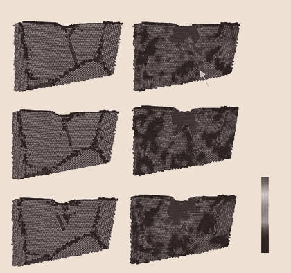
Cheong and Zhang [146]. Their simulations provide further details about the phase
transformations that occur in silicon as a result of nanoindentation. In particular,
they find that the diamond cubic silicon is transformed into a body-centered tetrag-
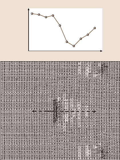
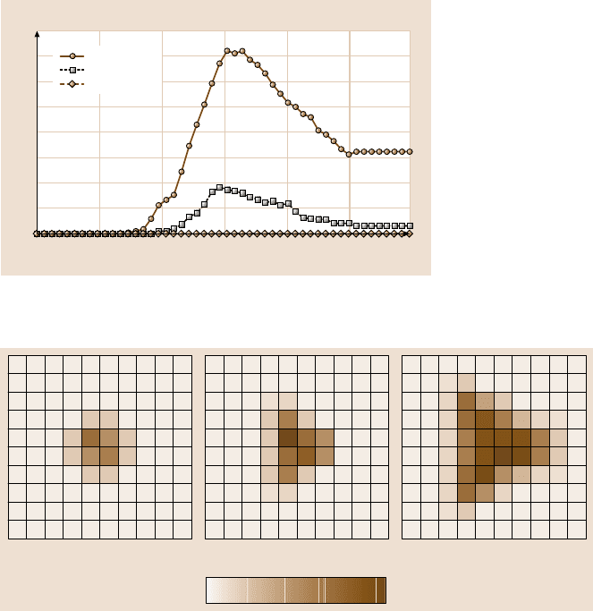
onal structure (β-Si) upon loading of the indenter, as illustrated in Fig. 13.12. Fig-
ure 13.13 shows that the coordination numbers of silicon atoms also coincide with
that of the theoreticalβ-Si structure. The body-centeredtetragonal structure is trans-
formed into amorphous silicon during the unloading stage. A second indentation
simulation again predicted that that this is a reversible process. Atomistic simulat-
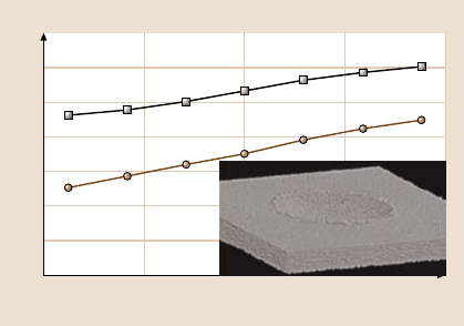
ions by Sanz-Navarro et al. [147] shows the relation between the indentation of
silicon and the hydrostatic pressure on surface cells due to the nanoindentation, as
illustrated in Fig. 13.14. These simulations further predict that the transformation
of diamond silicon into the β-Si structure can occur if the hydrostatic pressure is
somewhat over 12GPa.
Multimillion atom simulations of the indentation of silicon nitride were recently
carried out by Walsh et al. [148]. The elastic modulus and hardness of the surface
was calculated using load–displacement relationships. Snapshots from the simu-
lations, illustrated in Fig. 13.15, show that pile-up occurs on the surface along the
13 Computer Simulations of Nanometer-Scale Indentation and Friction 675
Fig. 13.12a–e. Snapshots of a silicon sample during indentation. The smaller dots are dia-
mond atoms. (a) Crystalline silicon prior to indentation. (b) Atoms beneath the indenter are
displaced as a result of indentation. (c) The system at maximum indentation. Some of the
atoms are in a crystalline arrangement (circled region)thatisdifferent from the diamond
structure. (d) The surface structure is largely amorphous as the tip is withdrawn. (e)The
surface after indentation. Note the amorphous region at the site of the indentation process.
After [130] with the permission of the IOP (2000)
edges of the tip. Plastic deformationof the surface is predicted to extenda significant
distance beyond the actual contact area of the indenter, as illustrated in Fig. 13.15.
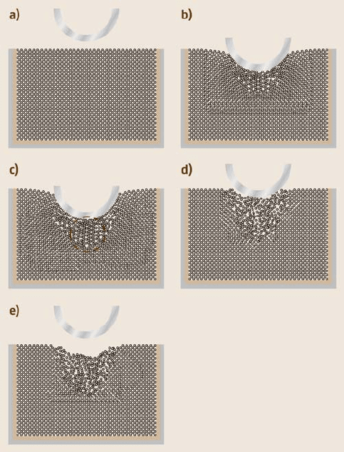
The indentation of bare and hydrogen-terminated diamond (111) surfaces be-
yond the elastic limit was investigated by Harrison et al. [149] using a hydrogen-
terminated sp
3
-bonded tip in MD simulations that utilized bond-order potentials.
The simulations identified the depth and applied force at which the diamond (111)
substrate incurred plastic deformation due to indentation.At low indentationforces,
the tip–surface interaction is purely elastic, as illustrated in Fig. 13.16. This find-
ing agrees with the findings of Cho et al. [150], who examined the atomic-scale
676 Susan B. Sinnott et al.
10
0
Time steps (× 100)
Number of atoms
100
200
300
400
500
600
700
800
490
90 170 250 330 410
6-coordinated
7-coordinated
8-coordinated
Fig. 13.13. The coordination of the silicon atoms shown in Fig. 13.12 as a function of time
during nanoindentation. After [146] with the permission of the IOP (2000)
0
Hydrostatic pressure (GPa)
184.5 9 13.5
a) b) c)
Fig. 13.14. Calculated hydrostatic pressure of surface cells at indentation depths of (a)8.9Å,
(b)15.7Å,and(c)25.3 Å. After [147] with the permission of the IOP (2000)
mechanical hysteresis experienced by an AFM tip indenting Si(100) with density
functional theory. The calculations predicted that at low rates it is possible to cycle
repeatedly between two buckled configurations of the surface without adhesion.
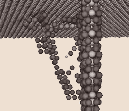
When the nanoindentation process of diamond (111) is plastic, connective
strings of atoms are formed between the tip and the surface, as illustrated in
Fig. 13.17. These strings break as the distance between the tip and crystal increases
and each break is accompanied by a sudden drop in the potential energy at large
positive values of tip–substrate separation. The simulations further predict that the
tip end twists to minimize interatomic repulsive interactions between the hydrogen
atoms on the surface and the tip. This behavior is predicted to lead to new covalent
bond formationbetween the tip and the carbon atoms below the first layer of the sur-
face and connective strings of atoms between the tip and the surface when the tip is