Bhushan B. Nanotribology and Nanomechanics: An Introduction
Подождите немного. Документ загружается.

4 Noncontact Atomic Force Microscopy and Related Topics 161
3nm 1nm
+9q
C
[1120]
a) b) c) d)
Fig. 4.19. (a) Image of the high-temperature, reconstructed clean α
−
Al
2
O
3
surface ob-
tained by using the constant-height mode. The rhombus represents the unit cell of the
(
√
31 ×
√
31)R + 9
◦
reconstructed surface. (b) Higher-magnification image of (a). Imaging
was performed at a reduced tip–sample distance. (c) Schematic representation of the indi-
cating regions of hexagonal order in the center of reconstructed rhombi. (d) Superposition
of the hexagonal domain with reconstruction rhombi found by NC-AFM imaging. Atoms in
the gray shaded regions are well ordered. The images and the schematic representations are
from [73]
2 nm
c
10 nm
b
a
ba
a) b) c)
Sr atom
Ti atom
O atom
[010]
[001]
Fig. 4.20. (a)STMand(b)NC-AFMimagesofaSrTiO
3
(100) surface. (c) A proposed model
of the SrTiO
3
(100)-(
√
5×
√
5)R26.6
◦
surface reconstruction. The images and the schematic
representations are from [84]
performed measurements using both STM and NC-AFM, and have found that the
size of the bright spots as observed by NC-AFM is always smaller than that for
STM measurement, and that the dark spots, which are not observed by STM, are
arranged along the [001] and [010] directions in the NC-AFM image. A theoreti-
cal simulation of the NC-AFM image using first-principles calculations shows that
the bright and dark spots correspond to Sr and oxygen atoms, respectively. It has
been proposed that the structural model of the reconstructed surface consists of an
ordered Sr adatom located at the oxygen fourfold site on the TiO
2
-terminated layer
(Fig. 4.20c).
Because STM images are related to the spatial distribution of the wave func-
tions near the Fermi level, atoms without a local density of states near the Fermi
level are generally invisible even on conductive materials. On the other hand, the
NC-AFM image reflects the strength of the tip–sample interaction force originat-
ing from chemical, electrostatic and other interactions. Therefore, even STM and
162 Franz J. Giessibl et al.
NC-AFM images obtained using an identical tip and sample may not be identical
generally. The simultaneous imaging of a metal oxide surface enables the inves-
tigation of a more detailed surface structure. The images of a TiO
2
(110) surface
simultaneously obtained with STM and NC-AFM [78] are a typical example. The
STM image shows that the dangling-bond states at the tip apex overlap with the
dangling bonds of the 3d states protruding from the Ti atom, while the NC-AFM
primarily imaged the uppermost oxygen atom.
Recently, calculations of the interaction of a Si tip with metal oxides surfaces,
such as Al
2
O
3
(0001), TiO
2
(110), and MgO(001), were reported [88,89]. Previous
simulations of AFM imaging of alkali halides and fluorides assume that the tip
would be oxides or contaminated and hence have been performed with a model
of ionic oxide tips. In the case of imaging a metal oxide surface, pure Si tips are
appropriate for a more realistic tip model because the tip is sputtered for cleaning
in many experiments. The results of ab initio calculations for a Si tip with a dan-
gling bond demonstrate that the balance between polarization of the tip and co-
valent bonding between the tip and the surface should determine the tip–surface
force. The interaction force can be related to the nature of the surface electronic
structure. For wide-gap insulators with a large valence-band offset that preventssig-
nificant electron-density transfer between the tip and the sample, the force is domi-
nated by polarization of the tip. When thegap is narrow, the charge transferincrease
and covalent bonding dominates the tip–sample interaction. The forces over anions
(oxygen ions) in the surface are larger than over cations (metal ions), as they play
a more significant role in charge transfer. This implies that a pure Si tip would al-
ways show the brightest contrast over the highest anions in the surface. In addition,
Fos te r et al. [88] suggested the method of using applied voltage, which controls the
charge transfer, during an AFM measurement to define the nature of tip apex.
The collaboration between experimental and theoretical studies has made great
progress in interpreting the imaging mechanism for binary insulators surface and
revealsthat a well-defined tip with atomic resolution is preferable for imaging a sur-
face.As described previously,a method for the evaluationof the natureof thetip has
been developed. However, the most desirable solution would be the development of
suitable techniques for well-defined tip preparation and a few attempts at controlled
production of Si tips have been reported [24,90,91].
4.4.2 Atomically Resolved Imaging of a NiO(001) Surface
The transition metal oxides, such as NiO, CoO, and FeO, feature the simultaneous
existence of an energy gap and unpaired electrons, which gives rise to a variety of
magnetic property. Such magnetic insulators are widely used for the exchange bias-
ing for magnetic and spintronic devices. NC-AFM enables direct surfaceimaging of
magnetic insulators on an atomic scale. The forces detected by NC-AFM originate
fromseveralkinds of interactionbetween the surface and thetip, includingmagnetic
interactions in some cases. Theoretical studies predict that short-range magnetic in-
teractions such as the exchange interaction should enable the NC-AFM to image
magnetic moments on an atomic scale. In this section, we will describe imaging of
4 Noncontact Atomic Force Microscopy and Related Topics 163
the antiferromagnetic NiO(001) surface using a ferromagnetic tip. Also, theoretical
studies of the exchange force interaction between a magnetic tip and a sample will
be described.
Theoretical Studies of the Exchange Force
In the system of a magnetic tip and sample, the interaction detected by NC-AFM
includes the short-range magneticinteraction in addition to the long-range magnetic
dipole interaction. The energyof the short-rangeinteraction dependson the electron
spin states ofthe atoms on the apex of the tip and the sample surface, and the energy
difference between spin alignments (parallel or anti-parallel) is referred to as the
exchange interaction energy. Therefore, the short-range magnetic interaction leads
to the atomic-scale magnetic contrast, depending on the local energy difference be-
tween spin alignments.
In the past, extensive theoretical studies on the short-range magnetic interaction
between a ferromagnetic tip and a ferromagnetic sample have been performed by
a simple calculation[92], atight-bindingapproximation[93] andfirst-principlescal-
culations [94]. In the calculations performed by Nakamura et al. [94], three-atomic-
layer Fe(001) films are used as a model for the tip and sample. The exchange force
is defined as the difference between the forces in each spin configuration of the tip
and sample (parallel and anti-parallel). The result of this calculation demonstrates
that the amplitude of the exchange force is measurable for AFM (about 0.1nN).
Also, they forecasted that the discrimination of the exchange force would enable
direct imaging of the magnetic moments on an atomic scale. Foster et al. [95] have
theoretically investigated the interaction between a spin-polarized H atom and a Ni
atom on a NiO(001) surface. They demonstrated that the difference in magnitude
in the exchange interaction between opposite-spin Ni ions in a NiO surface could
be sufficient to be measured in a low-temperature NC-AFM experiment. Recently,
first-principles calculation of the interaction of a ferromagnetic Fe tip with an NiO
surface has demonstrated that it should be feasible to measure the difference in ex-
change force between opposite-spin Ni ions [96].
Atomically Resolved Imaging Using Non-coated and Fe-coated Si Tips
The detection of the exchange interaction is a challenging task for NC-AFM appli-
cations. An antiferromagnetic insulator NiO single crystal that has regularly aligned
atom sites with alternating electron spin states is one of the best candidates to prove
the feasibility of detecting the exchange force for the following reason. NiO has an
antiferromagnetic AF
2
structure as the most stable below the Néel temperature of
525K. This well-defined magneticstructure, in which Ni atoms on the (001) surface
are arranged in a checkerboard pattern, leads to the simple interpretation of an image
containing the atomic-scale contrast originating in the exchange force. In addition,
a clean surface can easily be prepared by cleaving.
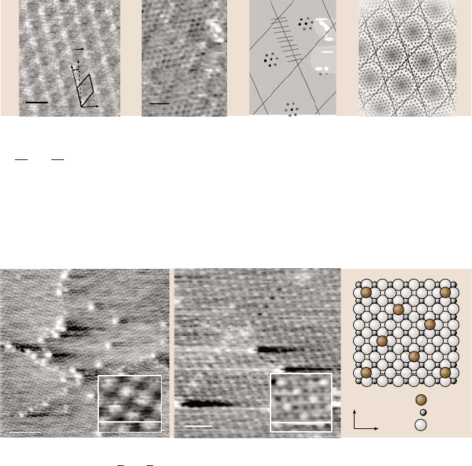
Figure 4.21a shows an atomically resolved image of a NiO(001) surface with
a ferromagnetic Fe-coated tip [97]. The bright protrusions correspond to atoms
spaced about 0.42 nm apart, consistent with the expected periodic arrangement of
164 Franz J. Giessibl et al.
Distance along [100] direction (nm)
Height (pm)
01234
50
40
30
20
10
a)
b)
[010]
[100]
Fig. 4.21. (a) Atomically
resolved image obtained with
an Fe-coated tip. (b)Shows
the cross sections of the
middle part in . Their corru-
gations are about 30 pm
the NiO(001) surface. The corrugation amplitude is typically 30pm, which is com-
parable to the value previously reported [82,83,98–100], as shown in Fig. 4.21b.
The atomic-resolution image (Fig. 4.21b), in which there is one maximum and one
minimum within the unit cell, resembles that of the alkali halide (001) surface. The
symmetry of the image reveals that only one type of atom appears to be at the max-
imum. From this image, it seems difficult to distinguish which of the atoms are
observed as protrusions. The theoretical works indicate that a metal tip interacts
strongly with the oxygen atoms on the MgO(001) surface [95]. From this result, it
is presumed that the bright protrusions correspond to the oxygen atoms. However,
it is still questionable which of the atoms are visible with a Fe-coated tip.
If the short-range magnetic interaction is included in the atomic image, the cor-
rugation amplitude of the atoms should depend on the direction of the spin over
the atom site. From the results of first-principles calculations [94], the contribution
of the short-range magnetic interaction to the measured corrugation amplitude is
expected to be about a few percent of the total interaction. Discrimination of such
small perturbations is therefore needed. In order to reduce the noise, the corruga-
tion amplitude was added on the basis of the periodicity of the NC-AFM image.
In addition, the topographical asymmetry, which is the index characterizing the dif-
4 Noncontact Atomic Force Microscopy and Related Topics 165
ference in atomic corrugation amplitude, has been defined [101]. The result shows
that the value of the topographical asymmetry calculated from the image obtained
with an Fe-coated Si tip depends on the direction of summing of the corrugation
amplitude, and that the dependency corresponds to the antiferromagnetic spin or-
dering of the NiO(001) surface [101, 102]. Therefore, this result implies that the
dependency of the topographical asymmetry originates in the short-range magnetic
interaction. However, in some cases the topographic asymmetry with uncoated Si
tips has a finite value [103]. The possibility that the asymmetry includes the influ-
ence of the structure of tip apex and of the relative orientation between the surface
and tip cannot be excluded. In addition, it is suggested that the absence of unam-
biguous exchange contrast is due to the fact that surface ion instabilities occur at
tip–sample distances that are small enough for a magnetic interact [100]. Another
possibility is that the magnetic properties of the tips are not yet fully controlled
because the topographic asymmetries obtained by Fe- and Ni-coated tips show no
significant difference [103]. In any cases, a careful comparison is needed to evaluate
the exchange interaction included in an atomic image.
From the aforementioned theoretical works, it is presumed that a metallic tip
has the capability to image an oxygen atom as a bright protrusion. Recently, the
magnetic properties of the NiO(001) surface were investigated by first-principles
electronic-structure calculations [104]. It was shown that the surface oxygen has
finite spin magnetic moment, which originates from symmetry breaking. We must
take into account the possibility that a metal atom at the ferromagnetic tip apex may
interact with a Ni atom on the second layer through a magnetic interaction mediated
by the electrons in an oxygen atom on the surface.
The measurements presented here demonstrate the feasibility of imaging mag-
netic structures on an atomic scale by NC-AFM. In order to realize explicit detection
of exchange force, further experiments and a theoretical study are required. In par-
ticular, the development of a tip with well-defined atomic structure and magnetic
properties is essential for exchange force microscopy.
4.5 Applications to Molecules
In the future, it is expected that electronic, chemical, and medical devices will be
downsized to the nanometer scale. To achieve this, visualizing and assembling in-
dividual molecular components is of fundamental importance. Topographic imag-
ing of nonconductive materials, which is beyond the range of scanning tunneling
microscopes, is a challenge for atomic force microscopy (AFM). Nanometer-sized
domains of surfactants terminated with different functional groups have been iden-
tified by lateral force microscopy (LFM) [107] and by chemical force microscopy
(CFM) [108] as extensions of AFM. At a higher resolution, a periodic array of
molecules, Langmuir–Blodgett films [109] for example, was recognized by AFM.
However, it remains difficult to visualize an isolated molecule, molecule vacancy,
or the boundary of different periodic domains, with a microscope with the tip in
contact.
166 Franz J. Giessibl et al.
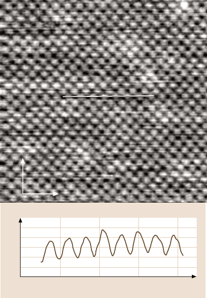
Fig. 4.22. The constant frequency-shift topography
of domain boundaries on a C
60
multilayered film
deposited on a Si(111) surface based on [105]. Im-
age size: 35×35 nm
2
4.5.1 Why Molecules and Which Molecules?
Accessto individualmolecules has notbeen a trivialtask even fornoncontactatomic
force microscopy (NC-AFM). The force pulling the tip into the surface is less sen-
sitive to the gap width (r), especially when chemically stable molecules cover the
surface. The attractive potential between two stable molecules is shallow and ex-
hibits r
−6
decay [13].
High-resolution topography of formate (HCOO
−
) [110] was first reported in
1997 as a molecular adsorbate. The number of imaged molecules is now increas-
ing because of the technological importance of molecular interfaces. To date, the
following studies on molecular topography have been published: C
60
[105, 111],
DNAs [106, 112], adenine and thymine [113], alkanethiols [113, 114], a pery-
lene derivative (PTCDA) [115], a metal porphyrin (Cu–TBPP) [116], glycine sul-
fate [117], polypropylene [118], vinylidene fluoride [119], and a series of carboxy-
lates (RCOO
−
) [120–126]. Two of these are presented in Figs. 4.22 and 4.23 to
demonstrate the current stage of achievement. The proceedings of the annual NC-
AFM conference represent a convenient opportunity for us to update the list of
molecules imaged.
4.5.2 Mechanism of Molecular Imaging
A systematic study of carboxylates (RCOO
−
) with R = H, CH
3
,C(CH
3
)
3
,C≡ CH,
and CF
3
revealed that the van der Waals force is responsible for the molecule-
dependent microscope topography despite its long-range (r
−6
) nature. Carboxy-
lates adsorbed on the (110) surface of rutile TiO
2
have been extensively studied
as a prototype for organic materials interfaced with an inorganic metal oxide [128].
A carboxylic acid molecule (RCOOH) dissociates on this surface to a carboxylate
(RCOO
−
)andaproton(H
+
) at room temperature, as illustrated in Fig. 4.24. The
pair of negatively charged oxygen atoms in the RCOO
−
coordinate two positively
charged Ti atoms on the surface. The adsorbed carboxylates create a long-range or-
dered monolayer. The lateral distances of the adsorbates in the ordered monolayer
4 Noncontact Atomic Force Microscopy and Related Topics 167
~0.33 nm
Distance (nm)
Height (pm)
027
0.5
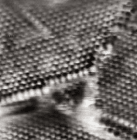
Fig. 4.23. The constant
frequency-shift topography
of a DNA helix on a mica sur-
face based on [106]. Image
size: 43×43 nm
2
.Theimage
revealed features with a spac-
ing of 3.3 nm, consistent with
the helix turn of B-DNA
[001]
a)
0.65 nm
H
0.15
H
H
0.11
0.46
Acetate
126°
OO
0.21
0.11
0.06
0.38 nm
Formate
OO
H
C
C
C
H
3
C
CH
3
C
HH
H
0.15
0.15
0.58
Pivalate
0.14
C
0.12
H
0.11
0.64
Propiolate
OO OO
C
CC
C
b)
F
0.15
F
F
0.13
0.46
OO
C
C
Trifluoroacetate
Ti Ti Ti Ti
Ti TiTi Ti Ti Ti
0.60 nm
[110]
Fig. 4.24. The carboxylates and TiO
2
substrate. (a) Top and side view of the ball model. Small
shaded and large shaded balls represent Ti and O atoms in the substrate. Protons yielded in
the dissociation reaction are not shown. (b) Atomic geometry of formate, acetate, pivalate,
propiolate, and trifluoroacetate adsorbed on the TiO
2
(110) surface. The O
−
Ti distance and
O
−
C
−
O angle of the formate were determined in the quantitative analysis using photoelec-
tron diffraction [127]
168 Franz J. Giessibl et al.
are regulated at 0.65 and 0.59nm along the [110] and [001] directions. By scanning
a mixed monolayer containing different carboxylates, the microscopetopographyof
the terminal groups can be quantitativelycomparedwhile minimizing tip-dependent
artifacts.
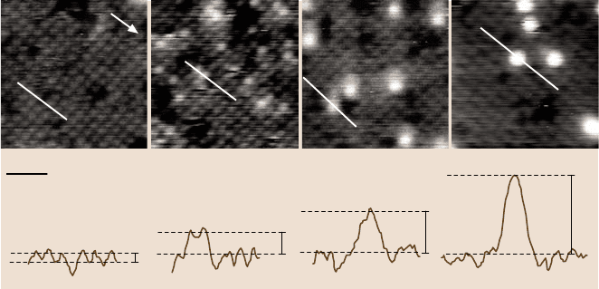
Figure 4.25 presents the observed constant frequency-shift topography of four
carboxylates terminated by different alkyl groups. On the formate-covered surface
of panel (a), individual formates (R
=
H) were resolved as protrusions of uniform
brightness. The dark holes represent unoccupied surface sites. The cross section in
the lower panel shows that the accuracy of the height measurement was 0.01nm or
better. Brighter particles appeared in the image when the formate monolayer was
exposed to acetic acid (CH
3
COOH) as shown in panel (b). Some formates were ex-
changed with acetates (R
=
CH
3
) impinging from the gas phase [129]. Because the
number of brighter spots increased with exposure time to acetic acid, the brighter
particle was assigned to the acetate [121]. Twenty-nine acetates and 188 formates
were identified in the topography. An isolated acetate and its surrounding formates
exhibited an image height difference of 0.06nm. Pivalate is terminated by bulky
R=(CH
3
)
3
. Nine bright pivalates were surrounded by formates of ordinary bright-
ness in the image of panel (c) [123]. The image height difference of an isolated
pivalate over the formates was 0.11nm. Propiolate with C≡CH is a needle-like ad-
sorbate of single-atom diameter. That molecule exhibited in panel (d) a microscope
topography 0.20nm higher than that of the formate [125].
The image topography of formate, acetate, pivalate, and propiolate followed the
order of the size of the alkyl groups. Their physical topography can be assumed
basedontheC
−
CandC
−
H bond lengths in the corresponding RCOOH molecules
in the gas phase [130], and is illustrated in Fig. 4.24. The top hydrogen atom of
2 nm
0.06 nm
0.20 nm
0.11 nm
0.02 nm
[001]
a) b) c) d)
Fig. 4.25. The constant frequency-shift topography of carboxylate monolayers prepared on
the TiO
2
(110) surface based on [121, 123,125]. Image size: 10 ×10 nm
2
.(a) Pure formate
monolayer; (b) formate–acetate mixed layer; (c) formate–pivalate mixed layer; (d)formate–
propiolate mixed layer. Cross sections determined on the lines are shown in the lower panel
4 Noncontact Atomic Force Microscopy and Related Topics 169
the formate is located 0.38 nm above the surface plane containing the Ti atom pair,
while three equivalent hydrogen atoms of the acetate are more elevated at 0.46nm.
The uppermost H atoms in the pivalate are raised by 0.58nm relative to the Ti
plane. The H atom terminating the triple-bonded carbon chain in the propiolate is at
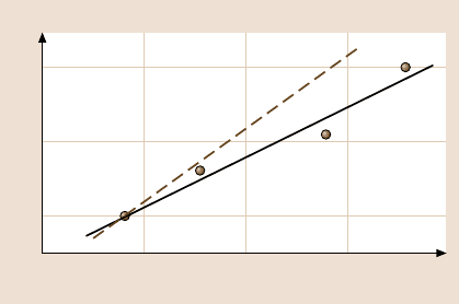
0.64nm. Figure 4.26summarizesthe observedimageheights relativeto the formate,
as a function of the physical height of the topmost H atoms given in the model. The
straight line fitted the four observations [122]. When the horizontal axis was scaled
with other properties (molecular weight, the number of atoms in a molecule, or the
number of electrons in valence states), the correlation became poor.
On the other hand, if the tip apex traced the contour of a molecule composed of
hard-sphere atoms, the image topographywould reproduce the physical topography
in a one-to-one ratio, as shown by the broken line in Fig. 4.26. However, the slope
of the fitted line was 0.7. A slope of less than unity is interpreted as the long-range
nature of the tip–molecule force. The observable frequency shift reflects the sum of
the forces between the tip apex and individualmolecules. When the tip passes above
a tall molecule embedded in short molecules, it is pulled up to compensate for the
increased force originating from the tall molecule. Forces between the lifted tip and
the short molecules are reduced due to the increased tip–surfacedistance. Feedback
regulation pushes down the probe to restore the lost forces.
This picture predictsthat microscopetopographyis sensitive to the lateral distri-
bution of the molecules, and that was in fact the case. Two-dimensionally clustered
acetates exhibited enhanced image height over an isolated acetate [121]. The tip–
molecule force therefore remained nonzero at distances over the lateral separation
of the carboxylateson this surface (0.59–0.65nm). Chemical bond interactionscan-
not be important across such a wide tip–molecule gap, whereas atom-scale images
of Si(111)(7×7) are interpreted with the fractional formation of tip–surface chemi-
cal bonds [24,45,49].Instead,the attractive componentof the van derWaals force is
probableresponsiblefor the observedmolecule-dependenttopography.The absence
of the tip–surface chemical bond is reasonable on the carboxylate-covered surface
terminated with stable C
−
H bonds.
0.70.60.50.40.3
0.2
0.1
0.0
Physical topography relative to Ti-plane (nm)
Microscope topography relative to formate (nm)
Fig. 4.26. The constant
frequency-shift topography
of the alkyl-substituted car-
boxylates as a function of
their physical topography
given in the model of Fig. 4.3
based on [123]
170 Franz J. Giessibl et al.
The attractive component of the van der Waals force contains electrostatic
terms caused by permanent-dipole/permanent-dipole coupling, permanent-dipole/
induced-dipole coupling, and induced-dipole/induced-dipole coupling (dispersion
force). The four carboxylates examined are equivalent in terms of their permanent
electric dipole, because the alkyl groups are non-polar. The image contrast of one
carboxylate relative to another is thus ascribed to the dispersion force and/or the
force created by the coupling between the permanent dipole on the tip and the in-
duced dipole on the molecule. If we further assume that the Si tip used exhibits
the smallest permanent dipole, the dispersion force remains dominant to create the
NC-AFM topography dependent on the non-polar groups of atoms. A numerical
simulation based on this assumption [125] successfully reproduced the propiolate
topography of Fig. 4.25d. A calculation that does not include quantum chemical
treatment is expected to work, unless the tip approaches the surface too closely, or
the molecule possesses a dangling bond.
In addition to the contribution of the dispersion force, the permanent dipole mo-
ment of molecules may perturb the microscope topography through electrostatic
coupling with the tip. Its possible role was demonstrated by imaging a fluorine-
substituted acetate. The strongly polarized C
−
F bonds were expected to perturb the
electrostatic field over the molecule. The constant frequency-shift topography of
acetate (R
=
CH
3
) and trifluoroacetate (R
=
CF
3
) was indeed sensitive to the fluorine
substitution. The acetate was observed to be 0.05nm higher than the trifluoroac-
etate [122], although the F atoms in the trifluoroacetate as well as the H atoms in
the acetate were lifted by 0.46nm from the surface plane, as illustrated in Fig. 4.24.
4.5.3 Perspectives
The experimental results summarized in this section prove the feasibility of us-
ing NC-AFM to identify individual molecules. A systematic study on the con-
stant frequency-shift topography of carboxylates with R=CH
3
,C(CH
3
)
3
,C≡ CH,
and CF
3
has revealed the mechanism behind the high-resolution imaging of the
chemically stable molecules. The dispersion force is primarily responsible for the
molecule-dependent topography. The permanent dipole moment of the imaged
molecule,if it exists,perturbsthe topographythroughthe electrostatic couplingwith
the tip. A tiny calculation containing empirical force fields works when simulating
the microscope topography.
These results make us optimistic about analyzing physical and chemical prop-
erties of nanoscale supramolecular assemblies constructed on a solid surface. If the
accuracy of topographic measurement is developed by one more order of magni-
tude, which is not an unrealistic target, it may be possible to identify structural
isomers, chiral isomers, and conformational isomers of a molecule. Kelvin probe
force microscopy(KPFM), an extensionof NC-AFM, providesa nanoscaleanalysis
of molecular electronic properties [118,119]. Force spectroscopy with chemically
modified tips seems promising for the detection of a selected chemical force. Op-
eration in a liquid atmosphere [131] is required for the observation of biochemical
materials in their natural environment.