Bhushan B. Nanotribology and Nanomechanics: An Introduction
Подождите немного. Документ загружается.


4 Noncontact Atomic Force Microscopy and Related Topics 151
dependence, between the dangling bond pointing out of the silicon dimer structure
on the Si(100)-(2×1) reconstructed surface and the dangling bond pointing out of
the apex of the silicon tip; a dimer structure is obtained with a larger separation than
between silicones on the surface.
The bright spots in Fig. 4.13 seem to be located at hydrogen atom sites on the
Si(100)-(2× 1):H monohydride surface, because the distance between the bright
spots forming the dimer structure (3.5±0.1Å) approximately agrees with the dis-
tance between the hydrogens, i.e., 3.52Å. Thus, the noncontact AFM atomically
resolved the individual hydrogen atoms on the topmost layer. On this surface, the
dangling bond is terminated by a hydrogen atom, and the hydrogen atom on the
topmost layer does not have chemical reactivity. Therefore, the interaction between
the hydrogen atom on the topmost layer and the apex of the silicon tip does not con-
tribute to the chemical bonding interaction with strong direction dependence as on
the silicon surface, and the bright spots in the noncontact AFM image correspondto
the hydrogen atom sites on the topmost layer.
4.3.3 Metal Deposited Si Surface
In this section, we will introduce the comparative study of force interactions be-
tween a Si tip and a metal-deposited Si surface, and between a metal adsorbed Si
tip and a metal-deposited Si surface [51,52]. As for the metal-deposited Si surface,
Si(111)-(
√
3×
√
3)-Ag (hereafter referred to as
√
3-Ag) surface was used.
For the
√
3-Ag surface, the honeycomb-chained trimer (HCT) model has been
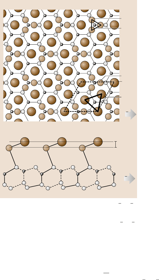
accepted as the appropriate model. As shown in Fig. 4.5, this structure contains a Si
trimer in the second layer, 0.75Å below the Ag trimer in the topmost layer. The
topmost Ag atoms and lower Si atoms form covalent bonds. The interatomic dis-
tances between the nearest-neighbor Ag atoms forming the Ag trimer and between
the lower Si atoms forming the Si trimer are 3.43Å and 2.31 Å, respectively. The
apexes of the Si trimers and Ag trimers face the [11
2] direction and the direction
tilted a little to the [
112] direction, respectively.
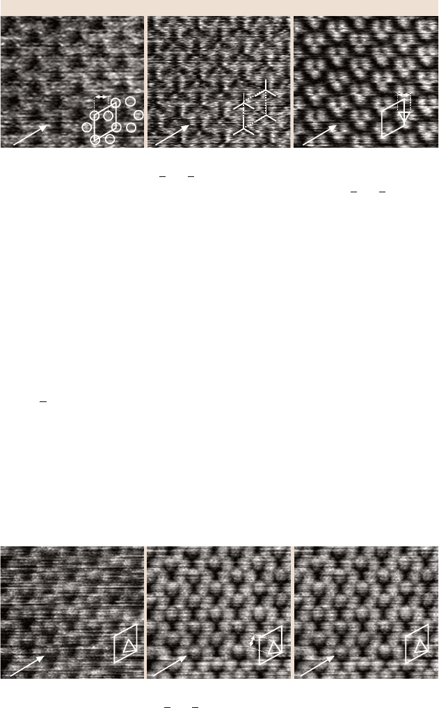
In Fig. 4.15, we show the noncontact AFM images measured using a normal
Si tip at a frequency shift of (a) −37Hz, (b) −43 Hz and (c) −51 Hz, respectively.
These frequency shifts correspond to tip–sample distances of about 0–3Å. We de-
fined the zero position of the tip–sample distance, i.e., the contact point, as the
point at which the vibration amplitude began to decrease. The rhombus indicates
the
√
3×
√
3 unit cell. When the tip approachedthe surface, the contrast of the non-
contact AFM images become strong and the pattern changed remarkably. That is,
by approachingthe tip toward the sample surface, the hexagonal pattern, the trefoil-
like pattern composed of three dark lines, and the triangle pattern can be observed
sequentially. In Fig. 4.15a, the distance between the bright spots is 3.9 ±0.2Å. In
Fig. 4.15c, the distance between the bright spots is 3.0±0.2Å, and the direction of
the apex of all the triangles composed of three bright spots is [11
2].
In Fig. 4.16, we show the noncontact AFM images measured by using Ag-
absorbed tip at a frequency shift of (a) −4.4Hz, (b) −6.9Hz and (c) −9.4Hz,
respectively. The tip–sample distances Z are roughly estimated to be Z = 1.9Å,
152 Franz J. Giessibl et al.
Top view
Side view
[112]
[112]
Si
2.31 Å
6.65 Å
Ag
3.43 Å
0.75 Å
Fig. 4.14. HCT model for the structure of the Si(111)-(
√
3×
√
3)–Ag surface. Black closed
circle, gray closed circle, open circle,andclosed circle with horizontal line indicate Ag atom
at the topmost layer, Si atom at the second layer, Si atom at the third layer, and Si atom at
the fourth layer, respectively. The rhombus indicates the
√
3×
√
3 unit cell. The thick, large,
solid triangle indicates an Ag trimer. The thin, small, solid triangle indicates a Si trimer
0.6Åand≈ 0 Å (in the noncontact region), respectively. When the tip approached
the surface, the pattern of the noncontact AFM images did not change, although the
contrast become clearer. A triangle pattern can be observed. The distance between
the brightspots is3.5±0.2Å. The direction ofthe apex of all thetriangles composed
of three bright spots is tilted a little from the [
112] direction.
Thus, noncontact AFM images measured on Si(111)-(
√
3 ×
√
3)-Ag surface
showed two types of distance dependence in the image patterns depending on the
atom species on the apex of the tip.
4 Noncontact Atomic Force Microscopy and Related Topics 153
a) b) c)
_
[112]
~3.0 Å
_
[112]
_
[112]
~3.9 Å
Fig. 4.15. Noncontact AFM images obtained at frequency shifts of (a) −37 Hz, (b) −43 Hz,
and (c) −51 Hz on a Si(111)-(
√
3×
√
3)–Ag surface. This distance dependence was obtained
with a Si tip. The scan area is 38Å×34 Å. A rhombus indicates the
√
3×
√
3 unit cell
By using the normal Si tip with a dangling bond, in Fig. 4.15a, the measured
distance between the bright spot of 3.9 ±0.2Å agrees with the distance of 3.84Å
between the centers of the Ag trimers in the HCT model within the experimental
error. Furthermore, the hexagonal pattern composed of six bright spots also agrees
with the honeycombstructure ofthe Ag trimer in HCT model. So the most appropri-
ate site corresponding to the bright spots in Fig. 4.15a is the site of the center of Ag
trimers. In Fig. 4.15c, the measured distance of 3.0±0.2Å between the bright spots
forming the triangle pattern agrees with neither the distance between the Si trimer
of 2.31Å nor the distance between the Ag trimer of 3.43Å in the HCT model, while
the direction of the apex of the triangles composed of three bright spots agrees with
the [11
2] direction of the apex of the Si trimer in the HCT model. So the most ap-
propriate site corresponding to the bright spots in Fig. 4.15c is the intermediate site
between the Si atoms and Ag atoms. On the other hand, by using the Ag-adsorbed
tip, the measured distance between the bright spots of 3.5±0.2Å in Fig. 4.16 agrees
with the distance of 3.43Å between the nearest-neighborAg atoms forming the Ag
trimer in the topmost layer in the HCT model within the experimental error. Further-
more, the direction of the apex of the triangles composed of three bright spots also
~3.5Å
a) b) c)
_
[112]
_
[112]
_
[112]
Fig. 4.16. Noncontact AFM images obtained at frequency shifts of (a) −4.4Hz,(b) −6.9Hz,
and (c) −9.4 Hz on a Si(111)-(
√
3×
√
3)-Ag surface. This distance dependence was obtained
with the Ag-adsorbed tip. The scan area is 38 Å×34 Å
154 Franz J. Giessibl et al.
agrees with the direction of the apex of the Ag trimer, i.e., tilted [112], in the HCT
model. So, the most appropriate site corresponding to the bright spots in Fig. 4.16
is the site of individual Ag atoms forming the Ag trimer in the topmost layer.
It should be noted that, by using the noncontact AFM with a Ag-adsorbed tip,
for the first time, the individual Ag atom on the
√
3-Ag surface could be resolved
in real space, although by using the noncontact AFM with an Si tip, it could not
be resolved. So far, the
√
3-Ag surface has been observed by a scanning tunneling
microscope (STM) with atomic resolution. However, the STM can also measure the
local chargedensity of statesnear the Fermilevelon the surface.From first-principle
calculations, it was proven that unoccupied surface states are densely distributed
around the center of the Ag trimer. As a result, bright contrast is obtained at the
center of the Ag trimer with the STM.
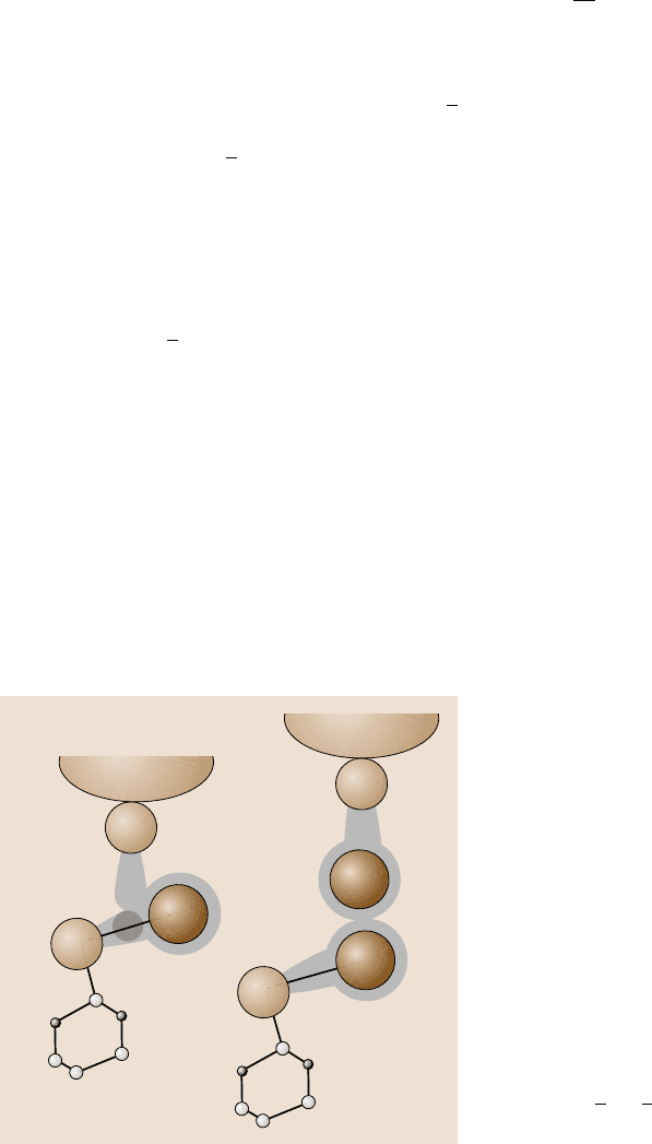
Finally,we considerthe originof theatomic-resolutionimaging ofthe individual
Ag atoms on the
√
3-Ag surface. Here, we discuss the difference between the force
interactions when using the Si tip and the Ag-adsorbed tip. As shown in Fig. 4.17a,
when using the Si tip, there is a dangling bond pointing out of the topmost Si atom
on the apex of the Si tip. As a result, the force interaction is dominated by phys-
ical bonding interactions, such as the Coulomb force, far from the surface and by
chemical bonding interaction very close to the surface. Namely, if a reactive Si tip
with a dangling bond approaches a surface, at distances far from the surface the
Coulomb force acts between the electron localized on the dangling bond pointing
out of the topmost Si atom on the apex of the tip, and the positive charge distributed
around the center of the Ag trimer. At distances very close to the surface, the chem-
ical bonding interaction will occur due to the onset of orbital hybridizationbetween
the dangling bond pointing out of the topmost Si atom on the apex of the Si tip and
a)
b)
Dangling
bond
Adsorbed
Ag atom
Si tip
Si
Ag
Si tip
Si
Si
Si
Ag
Ag
Fig. 4.17. Schematic illustra-
tion of (a) the Si atom with
dangling bond and (b)the
Ag-adsorbed tip above the
Si
−
Ag covalent bond on
a Si(111)-(
√
3 ×
√
3)-Ag
surface

4 Noncontact Atomic Force Microscopy and Related Topics 155
aSi
−
Ag covalent bond on the surface. Hence, the individual Ag atoms will not be
resolved and the image pattern will change depending on the tip–sample distance.
On the other hand, as shown in Fig. 4.17b, by using the Ag-adsorbed tip, the dan-
gling bond localized out of topmost Si atom on the apex of the Si tip is terminated
by the adsorbed Ag atom. As a result, even at very close tip–sample distances, the
force interaction is dominated by physical bonding interactions such as the vdW
force. Namely, if the Ag-adsorbed tip approaches the surface, the vdW force acts
between the Ag atom on the apex of the tip and the Ag or Si atom on the surface.
Ag atoms in the topmost layer of the
√
3-Ag surface are located higher than the Si
atoms in the lower layer. Hence, the individual Ag atoms (or their nearly true topog-
raphy) will be resolved, and the image pattern will not change even at very small
tip–sample distances. It should be emphasized that there is a possibility to identify
or recognize atomic species on a sample surface using noncontact AFM if we can
control the atomic species at the tip apex.
4.4 Applications to Insulators
Insulators such as alkali halides, fluorides, and metal oxides are key materials in
many applications, including optics, microelectronics, catalysis, and so on. Surface
properties are important in these technologies, but they are usually poorly under-
stood. This is due to their low conductivity, which makes it difficult to investigate
them using electron- and ion-based measurement techniques such as low-energy
electrondiffraction,ion-scatteringspectroscopy,and scanningtunnelingmicroscopy
(STM). Surface imaging by noncontact atomic force microscopy (NC-AFM) does
not require a sample surface with a high conductivity because NC-AFM detects
a force between the tip on the cantilever and the surface of the sample. Since the
first report of atomically resolved NC-AFM on a Si(111)-(7×7) surface [33], sev-
eral groups have succeeded in obtaining “true” atomic resolution images of insula-
tors, including defects, and it has been shown that NC-AFM is a powerful new tool
for atomic-scale surface investigation of insulators.
In this section we will describe typical results of atomically resolved NC-AFM
imaging of insulators such as alkali halides, fluorides and metal oxides. For the al-
kali halides and fluorides, we will focus on contrast formation, which is the most
important issue for interpreting atomically resolved images of binary compounds
on the basis of experimental and theoretical results. For the metal oxides, typical
examples of atomically resolved imaging will be exhibited and the difference be-
tween the STM and NC-AFM images will be demonstrated. Also, theoretical stud-
ies on the interaction between realistic Si tips and representative oxide surfaces will
be shown. Finally, we will describe an antiferromagnetic NiO(001) surface imaged
with a ferromagentic tip to explore the possibility of detecting short-range magnetic
interactions using the NC-AFM.
156 Franz J. Giessibl et al.
4.4.1 Alkali Halides, Fluorides and Metal Oxides
The surfaces of alkali halides were the first insulating materials to be imaged by
NC-AFM with “true” atomic resolution [53]. To date, there have been reports on
atomically resolved images of (001) cleaved surfaces for single-crystal NaF, RbBr,
LiF, KI, NaCl, [54], KBr [55] and thin films of NaCl(001) on Cu(111) [56]. In this
section we describe the contrast formation of alkali halides surfaces on the basis of
experimental and theoretical results.
Alkali Halides
In experiments on alkali halides, the symmetry of the observed topographic im-
ages indicates that the protrusions exhibit only one type of ions, either the positive
or negatively charged ions. This leads to the conclusion that the atomic contrast
is dominantly caused by electrostatic interactions between a charged atom at the
apex of the tip and the surface ions, i.e. long-range forces between the macroscopic
tip and the sample, such as the van der Waals force, are modulated by an alter-
nating short-range electrostatic interaction with the surface ions. Theoretical work
employing the atomistic simulation technique has revealed the mechanism for con-
trast formation on an ionic surface [57]. A significant part of the contrast is due to
the displacement of ions in the force field, not only enhancing the atomic corruga-
tions, but also contributing to the electrostatic potential by forming dipoles at the
surface. The experimentally observed atomic corrugation height is determined by
the interplay of the long- and short-range forces. In the case of NaCl, it has been ex-
perimentally demonstrated that a blunter tip produces a lager corrugation when the
tip–sample distance is shorter [54]. This result shows that the increased long-range
forces induced by a blunter tip allow for more stable imaging closer to the surface.
The stronger electrostatic short-range interaction and lager ion displacement pro-
duce a more pronounced atomic corrugation. At steps and kinks on an NaCl thin
film on Cu(111), the corrugation amplitude of atoms with low coordination number
has been observed to increase by a factor of up to two more than that of atomically
flat terraces [56]. The low coordination number of the ions results in an enhance-
ment of the electrostatic potential over the site and an increase in the displacement
induced by the interaction with the tip.
Theoretical study predicts that the image contrast depends on the chemical
species at the apex of the tip. Bennewitz et al. [56] have performed the calcula-
tions using an MgO tip terminated by oxygen and an Mg ion. The magnitude of
the atomic contrast for the Mg-terminated tip shows a slight increase in comparison
with an oxygen-terminated tip. The atomic contrast with the oxygen-terminated tip
is dominated by the attractive electrostatic interaction between the oxygen on the tip
apex and the Na ion, but the Mg-terminated tip attractively interacts with the Cl ion.
In other words, these results demonstrated that the species of the ion imaged as the
bright protrusions depends on the polarity of the tip apex.
These theoretical results emphasized the importanceof the atomic species at the
tip apex for the alkali halide (001) surface, while it is not straightforward to define
4 Noncontact Atomic Force Microscopy and Related Topics 157
the nature of the tip apex experimentally because of the high symmetry of the sur-
face structure. However, there are a few experiments exploring the possibilities to
determine the polarity of the tip apex. Bennewitz et al. [58] studied imaging of sur-
faces of a mixed alkali halide crystal, which was designed to observe the chemically
inhomogeneoussurface. The mixed crystal is composed of 60% KCl and 40% KBr,
with the Cl and Br ions interfused randomly in the crystal. The image of the cleaved
KCl
0.6
Br
0.4
(001) surface indicates that only one type of ion is imaged as protru-
sions, as if it were a purealkali halide crystal. However, the amplitude of the atomic
corrugation varies strongly between the positionsof the ions imaged as depressions.
This variation in the corrugations corresponds to the constituents of the crystal, i.e.
the Cl and Br ions, and it is concludedthat the tip apex is negativelycharged. More-
over, the deep depressionscan be assigned to Br ions by comparing the numberwith
the relative density of anions. The difference between Cl and Br anions with differ-
ent masses is enhanced in the damping signal measured simultaneously with the
topographic image [59]. The damping is recorded as an increase in the excitation
amplitude necessary to maintain the oscillation amplitude of the cantilever in the
constant-amplitude mode [56]. Although the dissipation phenomena on an atomic
scale are a subject under discussion, any dissipative interaction must generally in-
duce energy losses in the cantilever oscillation [60,61]. The measurement of energy
dissipation has the potential to enable chemical discrimination on an atomic scale.
Recently, a new procedure for species recognition on a alkali halide surface was
proposed [62]. This method is based on a comparison between theoretical results
and the site-specific measurement of frequency versus distance. The differences in
the force curves measured at the typical sites, such as protrusion, depression, and
their bridge position, are compared to the corresponding differences obtained from
atomistic simulation. The polarity of the tip apex can be determined, leading to the
identification of the surface species. This method is applicable to highly symmetric
surfaces and is useful for determining the sign of the tip polarity.
Fluorides
Fluorides are important materials for the progress of an atomic-scale-resolutionNC-
AFM imaging of insulators. There are reports in the literature of surface images for
single-crystal BaF
2
,SrF
2
[63], CaF
2
[64–66] and a CaF bilayer on Si(111) [67].
Surfaces of fluorite-type crystals are prepared by cleaving along the (111) planes.
Their structure is more complex than the structure of alkali halides, which have
a rock-salt structure. The complexity is of great interest for atomic-resolution imag-
ing using NC-AFM and also for theoretical predictions of the interpretation of the
atomic-scale contrast information.
The first atomically resolved images of a CaF
2
(111) surface were obtained in
topographic mode [65], and the surface ions mostly appear as spherical caps. Barth
et al. [68] have found that the CaF
2
(111) surface images obtained by using the
constant-height mode, in which the frequency shift is recorded with a very low loop
gain, can be categorized into two contrast patterns. In the first of these the ions
appear as triangles and in the second they have the appearance of circles, similar
158 Franz J. Giessibl et al.
to the contrast obtained in a topographic image. Theoretical studies demonstrated
that these two different contrast patterns could be explained as a result of imag-
ing with tips of different polarity [68–70]. When imaging with a positively charged
(cation-terminated) tip, the triangular pattern appears. In this case, the contrast is
dominated by the strong short-range electrostatic attraction between the positive tip
and the negative F ions. The cross section along the [121] direction of the trian-
gular image shows two maxima: one is a larger peak over the F(I) ions located in
the topmost layer and the other is a smaller peak at the position of the F(III) ions
in the third layer. The minima appear at the position of the Ca ions in the second
layer. When imaging with a negatively charged (anion-terminated)tip, the spherical
image contrast appears and the main periodicity is created by the Ca ions between
the topmost and the third F ion layers. In the cross section along the [121] direction,
the large maxima correspond to the Ca sites because of the strong attraction of the
negative tip and the minima appear at the sites of maximum repulsion over the F(I)
ions. At a position between two F ions, there are smaller maxima. This reflects the
weaker repulsion over the F(III) ion sites compared to the protruding F(I) ion sites
and a slower decay in the contrast on one side of the Ca ions.
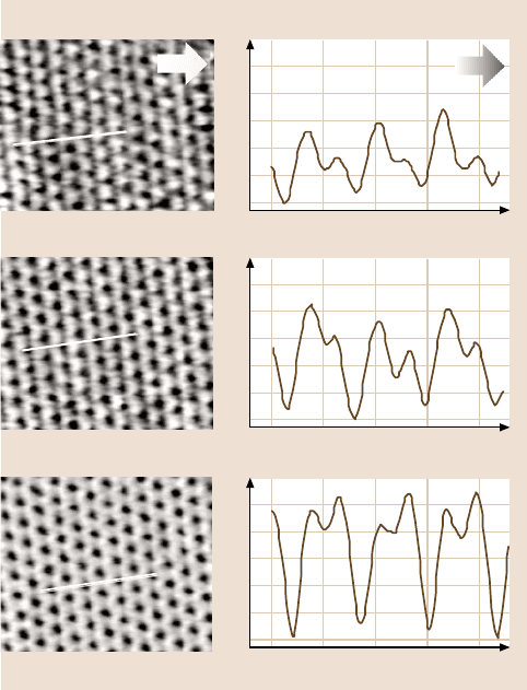
The triangularpattern obtainedwith a positively charged tip appearsat relatively
large tip–sample distance, as shown in Fig. 4.18a. The cross section along the [121]
direction,experimentresultsand theoretical studies bothdemonstratethe large-peak
andsmall-shouldercharacteristicfor thetriangularpatternimage (Fig.4.18d).When
the tip approaches the surface more closely, the triangular pattern of the experi-
mental images is more vivid (Fig. 4.18b), as predicted in the theoretical works. As
the tip approaches, the amplitude of the shoulder increases until it is equal to that
of the main peak, and this feature gives rise to the honeycomb pattern image, as
shown in Fig. 4.18c. Moreover, theoretical results predict that the image contrast
changes again when the tip apex is in close proximity to surface. Recently, Giessibl
et al. [71] achieved atomic imaging in the repulsive region and proved experimen-
tally the predicted change of the image contrast. As described here, there is good
correspondence in the distance dependency of the image obtained by experimental
and theoretical investigations.
From detailed theoretical analysis of the electrostatic potential [72], it was sug-
gested that the change in displacement of the ions due to the proximity of the tip
plays an importantrole in the formation of the image contrast. Such a drastic change
in image contrast, depending on both the polarity of the terminated tip atom and on
the tip–sample distance, is inherent to the fluoride (111) surface, and this image-
contrast feature cannot be seen on the (001) surface of alkali halides with a simple
crystal structure.
The results of careful experiments show another feature: that the cross sections
taken along the three equivalent [121] directions do not yield identical results [68].
It is thought that this can be attributed to the asymmetry of the nanocluster at the
tip apex, which leads to different interactions in the equivalent directions. A bet-
ter understanding of the asymmetric image contrast may require more complicated
modeling of the tip structure. In fact, it should be mentioned that perfect tips on an
4 Noncontact Atomic Force Microscopy and Related Topics 159
Detuning (Hz)
Distance (nm)
a)
b)
c)
d)
e)
f)
10
8
6
4
2
0
0.0 0.5 1.0 1.5 2.0
0.0 0.5 1.0 1.5 2.0
0.0 0.5 1.0 1.5 2.0
10
8
6
4
2
0
10
8
6
4
2
0
Fig. 4.18. (a)–(c)CaF
2
(111) surface images obtained by using the constant-height mode.
From (a)to(c) the frequency shift was lowered. The white lines represent the positions of
the cross section. (d)–(f) The cross section extracted from the Fourier-filtered images of (a)–
(c). The white and black arrows represent the scanning direction. The images and the cross
sections are from [68]
atomic scale can occasionally be obtained. These tips do yield identical results in
forwardand backwardscanning, and cross sections in thethree equivalentdirections
taken with this tip are almost identical [74].
The fluoride (111) surface is an excellent standard surface for calibrating tips on
an atomic scale. The polarity of the tip-terminated atom can be determined from the
image contrast pattern (spherical or triangular pattern). The irregularities in the tip
structurecan be detected,since the surface structure is highly symmetric. Therefore,
once such a tip has been prepared, it can be used as a calibrated tip for imaging
unknown surfaces.
The polarity and shape of the tip apex play an important role in interpreting NC-
AFM images of alkali halide and fluorides surfaces. It is expected that the achieve-

160 Franz J. Giessibl et al.
ment of good correlation between experimental and theoretical studies will help to
advance surface imaging of insulators by NC-AFM.
Metal Oxides
Most of the metal oxides that have attracted strong interest for their technological
importance are insulating. Therefore, in the case of atomically resolved imaging of
metal oxide surfaces by STM, efforts to increase the conductivity of the sample are
needed, such as, the introduction of anions or cations defects, doping with other
atoms and surface observationsduring heating of the sample. However,in principle,
NC-AFM provides the possibility of observing nonconductivemetal oxides without
these efforts. In cases where the conductivity of the metal oxides is high enough for
a tunneling current to flow, it should be noted that most surface images obtained by
NC-AFM and STM are not identical.
Since the first report of atomically resolved images on a TiO
2
(110) surface with
oxygen pointdefects [75], they havealso been reported on rutile TiO
2
(100)[76–78],
anataseTiO
2
(001)thinfilmonSrTiO
3
(100)[79]andonLaAO
3
(001)[80],SnO
2
(110)
[81],NiO(001)[82,83],SrTiO
3
(100)[84],CeO
2
(111)[85]andMoO
3
(010)[86]sur-
faces. Also, Barth et al. have succeeded in obtaining atomically resolved NC-AFM
imagesof acleanα
−
Al
2
O
3
(0001)surface[73]andofaUHVcleavedMgO(001)[87]
surface, which are impossible to investigate using STM. In this section we describe
typical results of the imaging of metal oxides by NC-AFM.
The α
−
Al
2
O
3
(0001) surface exists in several ordered phases that can reversibly
be transformed into each other by thermal treatments and oxygen exposure. It is
known that the high-temperature phase has a large (
√
31×
√
31)R±9
◦
unit cell.
However, the details of the atomic structure of this surface have not been revealed,
and two models have been proposed. Barth et al. [73] have directly observed this
reconstructed α
−
Al
2
O
3
(0001) surface by NC-AFM. They confirmed that the dom-
inant contrast of the low-magnification image corresponds to a rhombic grid repre-
senting a unit cell of (
√
31×
√
31)R+ 9
◦
, as shown in Fig. 4.19a. Also, more de-
tails of the atomic structures were determined from the higher-magnification image
(Fig. 4.19b), which was taken at a reduced tip–sample distance. In this atomically
resolved image, it was revealed that each side of the rhombus is intersected by ten
atomic rows, and that a hexagonal arrangement of atoms exists in the center of the
rhombi (Fig. 4.19c). This feature agrees with the proposed surface structure that
predicts order in the center of the hexagonal surface domains and disorder at the
domain boundaries. Their result is an excellent demonstration of the capabilities of
the NC-AFM for the atomic-scale surface investigation of insulators.
The atomic structure of the SrTiO
3
(100)-(
√
5x×
√
5)R26.6
◦
surface, as well as
that of Al
2
O
3
(0001)can be determined on the basis of the results of NC-AFM imag-
ing [84]. SrTiO
3
is one of the perovskite oxides, and its (100) surface exhibits the
many differentkinds of reconstructedstructures.In the case of the (
√
5×
√
5)R26.6
◦
reconstruction, the oxygen vacancy–Ti
3+
–oxygen model (where the terminated sur-
face is TiO
2
and the observed spots are related to oxygen vacancies) was proposed
from the results of STM imaging. As shown in Fig. 4.20, Kubo et al. [84] have