Bhushan B. Nanotribology and Nanomechanics: An Introduction
Подождите немного. Документ загружается.

120 Jason H. Hafner
3.2.7 Carbon Nanotube Tips
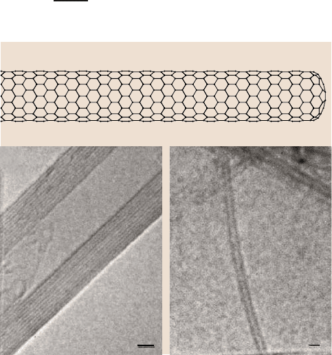
Carbon nanotubes are microscopic graphitic cylinders that are nanometers in diam-
eter, yet many microns in length. Single-walled carbon nanotubes (SWNT) consist
of singlesp
2
hybridizedcarbon sheets rolled into seamless tubes and have diameters
ranging from 0.7 to 3nm.
Carbon Nanotube Structure
Larger structures called multiwalled carbon nanotubes (MWNT) consist of nested,
concentrically arranged SWNT and have diameters ranging from 3 to 50 nm. Fig-
ure 3.8showsa model of nanotubestructure,as well as TEMimages of a SWNT and
a MWNT. The small diameter and high aspect ratio of carbon nanotubes suggests
their application as high resolution, high-aspect-ratio AFM probes.
Carbon Nanotube Mechanical Properties
Carbon nanotubes possess exceptional mechanical properties that impact their use
as probes. Their lateral stiffnesscan be approximatedfrom that of a solid elastic rod:
k
lat
=
3πYr
4
4l
3
, (3.4)
Fig. 3.8. The structure of carbon nanotubes, including TEM images of a MWNT (left)and
aSWNT(right), from [16]

3 Probes in Scanning Microscopies 121
where the spring constantk
lat
represents the restoring force per unit lateral displace-
ment, r is the radius, l is the length, and Y is the Young’s modulus (also called the
elastic modulus) of the material. For the small diameters and extreme aspect ratios
of carbon nanotube tips, the thermal vibrations of the probe tip at room temperature
can become sufficient to degrade image resolution. These thermal vibrations can be
approximated by equating
1
2
k
B
T of thermal energy to the energy of an oscillating
nanotube:
1
2
k
B
T =
1
2
k
lat
a
2
, (3.5)
where k
B
is Boltzmann’s constant, T is the temperature, and a is the vibration am-
plitude. Substituting for k
lat
from (3.4) yields:
a =
4k
B
Tl
3
3πYr
4
. (3.6)
The strong dependence on radius and length reveals that one must carefully control
the tip geometry at this size scale. Equation (3.6) implies that the stiffer the mate-
rial, i.e., the higher its Young’s modulus, the smaller the thermal vibrations and the
longer and thinner a tip can be. The Young’s moduli of carbon nanotubes have been
determined by measurements of the thermal vibration amplitude by TEM [18,19]
and by directly measuring the forces required to deflect a pinned carbon nanotube
in an AFM [20]. These experiments revealed that the Young’s modulus of carbon
nanotubes is 1–2 TPa, in agreement with theoretical predictions [21]. This makes
carbon nanotubes the stiffest known material and, therefore, the best for fabricating
thin, high-aspect-ratio tips. A more detailed and accurate derivation of the thermal
vibration amplitudes was derived for the Young’s modulus measurements [18,19].
Carbon nanotubes elastically buckle under large loads, rather than fracture or
plastically deform like most materials. Nanotubes were first observed in the buck-
led state by transmission electron microscopy [17], as shown in Fig. 3.9. The first
experimental evidence that nanotube buckling is elastic came from the application
of nanotubes as probe tips [22],described in detail below. A more direct experimen-
tal observation of elastic buckling was obtained by deflecting nanotubes pinned to
a low friction surface with an AFM tip [20]. Both reports found that the buckling
force could be approximated with the macroscopic Euler buckling formula for an
elastic column:
F
Euler
=
π
3
Yr
4
4l
2
. (3.7)
The buckling force puts another constraint on the tip length: If the nanotube is too
long the bucklingforcewill be too low for stable imaging. Theelastic buckling prop-
erty of carbon nanotubes has significant implications for their use as AFM probes.
If a large force is applied to the tip inadvertently, or if the tip encounters a large
step in sample height, the nanotube can buckle to the side, then snap back without
degraded imaging resolution when the force is removed, making these tips highly
robust. No other tip material displays this buckling characteristic.

122 Jason H. Hafner
1.2 nm
1 nm
Fig. 3.9. TEM images and a model of a buckled
nanotube, adapted from [17]
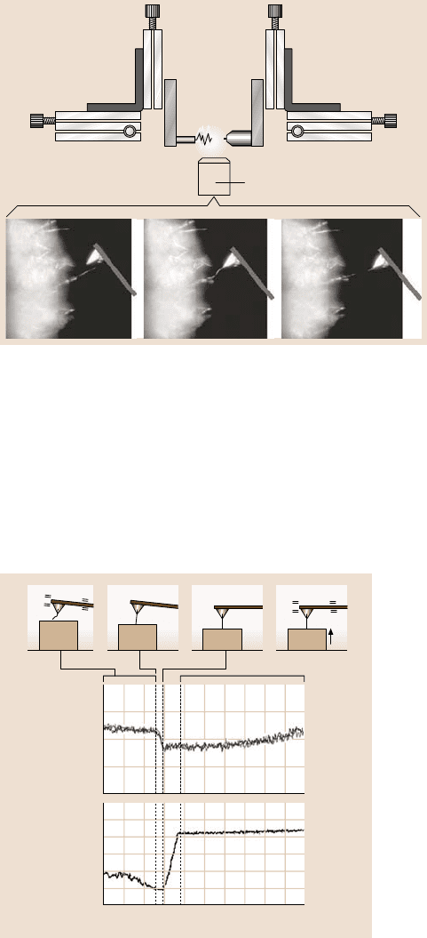
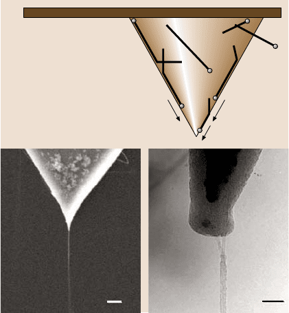
Manually Assembled Nanotube Probes
The first carbon nanotube AFM probes [22] were fabricated by techniques devel-
oped for assembling single-nanotube field emission tips [23]. This process, illus-
trated in Fig. 3.10, used purified MWNT material synthesized by the carbon arc
procedure. The raw material, which must contain at least a few percent of long
nanotubes (> 10µm) by weight, purified by oxidation to approximately 1% of its
original mass. A torn edge of the purified material was attached to a micromanipu-
lator by carbon tape and viewed under a high power optical microscope. Individual
nanotubes and nanotubebundles were visible as filamentsunder dark field illumina-
tion. A commercially available AFM tip was attached to another micromanipulator
opposing the nanotube material. Glue was applied to the tip apex from high vacuum
carbon tape supporting the nanotube material. Nanotubes were then manually at-
tached to the tip apex by micromanipulation. As assembled, MWNT tips were often
too long for imaging due to thermal vibrations and low buckling forces described in
Sect. 3.2.7. Nanotubes tips were shortened by applying 10V pulses to the tip while
it was near a sputtered niobium surface. This process etched ∼ 100nm lengths of
nanotube per pulse.
The manually assembled MWNT tips demonstrated several important nanotube
tip properties [22]. First, the high aspect ratio of the MWNT tips allowed the accu-
rate imaging of trenches in silicon with steep sidewalls, similar to FIB and EBD
tips. Second, elastic buckling was observed indirectly through force curves (see
3 Probes in Scanning Microscopies 123
50 × 0.6
Fig. 3.10. A schematic drawing of the setup for manual assembly of carbon nanotube tips
(top) and optical microscopy images of the assembly process (the cantilever was drawn in for
clarity)
Fig. 3.11). Note that as the tip taps the sample, the amplitudedrops to zero and a DC
deflection is observed, because the nanotube is unbuckled and is essentially rigid.
As the tip moves closer, the force on the nanotube eventually exceeds the buckling
force. The nanotube buckles, allowing the vibration amplitude to partially recover,
Deflection
(3.5 nm/div)
Z-position (10 nm/div)
Amplitude
(2 nm/div)
Fig. 3.11. Nanotube tip buck-
ling. Top diagrams corre-
spond to labeled regions
of the force curves. As the
nanotube tip buckles, the
deflection remains constant
and the amplitude increases,
from [16]
124 Jason H. Hafner
and the deflection remains constant. Numeric tip trajectory simulations could only
reproduce these force curves if elastic buckling was included in the nanotube re-
sponse. Finally, the nanotube tips were highly robust. Even after “tip crashes” or
hundreds of controlled buckling cycles, the tip retained its resolution and high as-
pect ratio.
Manual assembly of carbon nanotube probe tips is straightforward, but has sev-
eral limitations. It is labor intensive and notamenable to mass production.Although
MWNT tips have been made commercially available by this method, they are about
ten times more expensivethan silicon probes. The manualassembly method has also
been carried out in an SEM, rather than an optical microscope [24]. This eliminates
the need for pulse-etching, since short nanotubes can be attached to the tip, and the
“glue” can be applied by EBD. But this is still not the key to mass production, since
nanotube tips are made individually. MWNT tips provided a modest improvement
in resolution on biological samples, but typical MWNT radii are similar to that of
silicon tips, so they cannot provide the ultimate resolution possible with a SWNT
tip. SWNT bundles can be attached to silicon probes by manual assembly. Pulse
etching at times produces very high resolution tips that likely result from expos-
ing a small number of nanotubes from the bundle, but this is not reproducible [25].
Even if a sample could be prepared that consisted of individual SWNT for man-
ual assembly, such nanotubes would not be easily visible by optical microscopy or
SEM.
CVD Nanotube Probe Synthesis
The problems of manual assembly of nanotube probes discussed above can largely
be solved by directly growing nanotubes onto AFM tips by metal-catalyzed chem-
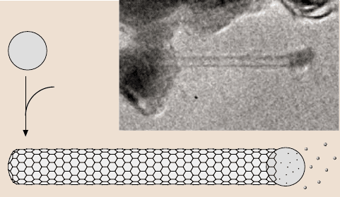
ical vapor deposition (CVD). The key features of the nanotube CVD process are
illustrated in Fig. 3.12. Nanometer-scale metal catalyst particles are heated in a gas
C
2
H
4
700–1000°C
Fig. 3.12. CVD nanotube synthesis. Ethylene reacts with a nanometer-scale iron catalyst
particle at high temperature to form a carbon nanotube. The inset in the upper right is a TEM
image showing a catalyst particle at the end of a nanotube, from [16]
3 Probes in Scanning Microscopies 125
mixture containing hydrocarbon or CO. The gas molecules dissociate on the metal
surface, and carbon is adsorbed into the catalyst particle. When this carbon precipi-
tates, it nucleates a nanotube of similar diameter to the catalyst particle. Therefore,
CVD allows control over nanotube size and structure, including the production of
SWNTs [26] with radii as low as 3.5 Angstrom [27].
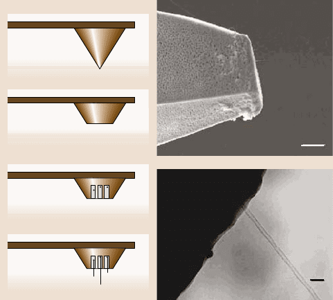
Several key issues must be addressed to grow nanotube AFM tips by CVD:
(1) the alignment of the nanotubes at the tip, (2) the number of nanotubes that grow
at the tip, and (3) the length of the nanotube tip. Li et al. [28] found that nano-
tubes grow perpendicular to a porous surface containing embedded catalyst. This
approach was exploited to fabricate nanotube tips by CVD [29] with the proper
alignment, as illustrated inFig. 3.13.A flattened area of approximately1–5µm
2
was
created on Si tips by scanning in contact mode at high load (1 µN) on a hard, syn-
thetic diamond surface. The tip was then anodized in HF to create 100 nm-diameter
pores in this flat surface [30]. It is important to only anodize the last 20–40µmof
the cantilever, which includes the tip, so that the rest of the cantilever is still reflec-
tive for use in the AFM. This was achieved by anodizing the tip in a small drop
of HF under the view of an optical microscope. Next, iron was electrochemically
deposited into the pores to form catalyst particles [31]. Tips prepared in this way
were heated in low concentrations of ethylene at 800
◦
C, which is known to favor
the growth of thin nanotubes [26]. When imaged by SEM, nanotubes were found
Fig. 3.13. Pore-growth CVD nanotube tip fabrication. The left panel, from top to bottom,
shows the steps described in the text. The upper right is an SEM image of such a tip with
a small nanotube protruding from the pores (scale bar is 1 µm). The lower right is a TEM of
a nanotube protruding from the pores (scale bar is 20 nm), from [16]
126 Jason H. Hafner
to grow perpendicular to the surface from the pores as desired (Fig. 3.13). TEM re-
vealed that the nanotubes were thin, individual, multiwalled nanotubes with typical
radii ranging from 3–5nm. If nanotubes did not grow in an acceptable orientation,
the carbon could be removed by oxidation, and then CVD repeated to grow new
nanotube tips.
These “pore-growth” CVD nanotube tips were typically several microns in
length – too long for imaging – and were pulse-etched to a usable length of
< 500nm. The tips exhibitedelastic buckling behaviorand were very robustin imag-
ing. In addition, the thin, individual nanotube tips enabled improved resolution [29]
on isolated proteins. The pore-growth method demonstrated the potential of CVD
to simplify the fabrication of nanotube tips, although there were still limitations. In
particular, the porous layer was difficult to prepare and rather fragile.
An alternative approach for CVD fabrication of nanotube tips involves direct
growth of SWNTs on the surface of a pyramidal AFM tip [32,33]. In this “surface-
growth” approach, an alumina/iron/molybdenum-powdered catalyst known to pro-
duce SWNT [26] was dispersed in ethanol at 1mg/mL. Silicon tips were dipped in
this solution and allowed to dry, leaving a sparse layer of ∼100nm catalyst clusters
on the tip. When CVD conditions wereapplied, single-walled nanotubesgrewalong
the silicon tipsurface.At a pyramidedge,nanotubescan either bend to alignwith the
edge,or protrude fromthe surface.If the energyrequired to bendthe tube and follow
the edge is less than the attractive nanotube-surface energy, then the nanotube will
follow the pyramid edge to the apex. Therefore, nanotubes were effectively steered
toward the tip apex by the pyramid edges. At the apex, the nanotube protruded from
the tip, since the energetic cost of bending around the sharp silicon tip was too high.
The high aspect ratio at the oxide-sharpened silicon tip apex was critical for good
nanotube alignment. A schematic of this approach is shown in Fig. 3.14. Evidence
for this model came from SEM investigationsthat show that a very high yield of tips
contains nanotubes only at the apex, with very few protruding elsewhere from the
pyramid. TEM analysis demonstrated that the tips typically consist of small SWNT
bundles that are formed by nanotubes coming together from different edges of the
pyramid to join at the apex, supporting the surface growth model described above
(Fig. 3.14). The “surface growth” nanotube tips exhibit a high aspect ratio and high
resolution imaging, as well as elastic buckling.
The surface growth method has been expanded to include wafer-scale produc-
tion of nanotube tips with yields of over 90% [34], yet one obstacle remains to
the mass production of nanotube probe tips. Nanotubes protruding from the tip are
several microns long, and since they are so thin, they must be etched to less than
100nm. While the pulse-etching step is fairly reproducible, it must be carried out
on nanotube tips in a serial fashion, so surface growth does not yet represent a true
method of batch nanotube tip fabrication.
Hybrid Nanotube Tip Fabrication: Pick-up Tips
Another method of creating nanotube tips is something of a hybrid between assem-
bly and CVD. The motivation was to create AFM probes that have an individual
3 Probes in Scanning Microscopies 127
a)
b) c)
Fig. 3.14a–c. Surface-growth
nanotube tip fabrication.
(a) Schematic represents the
surface growth process in
which nanotubes growing on
the pyramidal tip are guided
to the tip apex. (b),(c)Images
show (b) SEM (200-nm-scale
bar) and (c) TEM (20-nm-
scale bar) images of a surface
growth tip, from [16]
SWNT at the tip to achieve the ultimate imaging resolution. In order to synthe-
size isolated SWNT, they must be nucleated at sites separated farther than their
typical length. The alumina-supported catalyst contains a high density of catalyst
particles per 100 nm cluster, so nanotube bundles cannot be avoided. To fabricate
completely isolated nanotubes, isolated catalyst particles were formed by dipping
a silicon wafer in an isopropyl alcohol solution of Fe(NO
3
)
3
.Thiseffectively left
a submonolayer of iron on the wafer, so that when it was heated in a CVD fur-
nace, the iron became mobile and aggregated to form isolated iron particles. During
CVD conditions, these particles nucleated and grew SWNTs. By controlling the
reaction time, the SWNT lengths were kept shorter than their typical separation,
so that the nanotubes never had a chance to form bundles. AFM analysis of these
samplesrevealed1–3nm-diameterSWNT and un-nucleatedparticleson the surface
(Fig. 3.15). However, there were tall objects that were difficult to image at a density
of about 1 per 50µm
2
. SEM analysis at an oblique angle demonstrated that these
were SWNTs that had grown perpendicular to the surface (Fig. 3.15).
In the “pick-up tip” method, these isolated SWNT substrates were imaged by
AFM with silicon tips in air [9]. When the tip encountered a vertical SWNT, the
oscillation amplitude was damped, so the AFM pulled the sample away from the tip.
This pulled the SWNT into contact with the tip along its length, so that it became
attached to the tip. This assembly process happened automatically when imaging in
tapping mode – no special tip manipulation was required. When imaging a wafer
with the density shown in Fig. 3.15, one nanotube was attached per 8µm × 8 µm
scan at 512×512 and 2Hz, so a nanotube tip could be made in about 5min. Since
the as-formed SWNT tip continued to image, there was usually no evidence in the
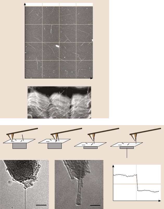
128 Jason H. Hafner
(μm)
0 2.5 7.5
–10.0
–7.5
–5.0
–2.5
0
5.0
10.0
Fig. 3.15. Atomic force mi-
croscopy image (top)of
a wafer with isolated nano-
tubes synthesized by CVD.
The SEM view provides ev-
idence that some of these
nanotubes are arranged verti-
cally
Z (50 nm/div)
Time (10 ms/div)
Fig. 3.16. Pick-up tip assembly of nanotube probes. The top illustrates the nanotube pick-
up process that occurs while imaging vertical nanotubes in an AFM, including a trace of
the Z-position during a pick-up event. The lower left TEM images show single nanotubes
(diameters 0.9nmand2.8 nm) on an AFM tip fabricated by this method, adapted from [9]
topographic image that a nanotube had been attached. However, the pick-up event
was identified when the Z-voltage suddenly stepped to larger tip-sample separation
due to the effective increase in tip length.
Individual SWNT tips must be quite short, typically less than 50nm in length,
for reasons outlined above. Pulse-etching, which removes 50–100nm of nanotube
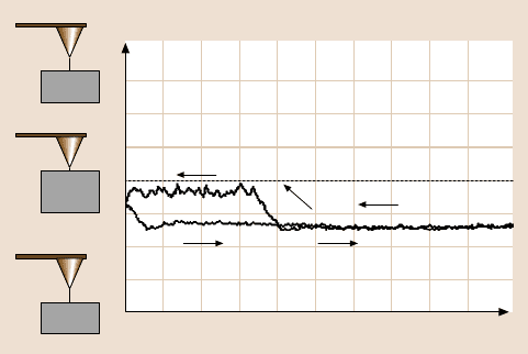
3 Probes in Scanning Microscopies 129
C
Deflection (3.7 nm/div)
Z-position (5 nm/div)
B
C
A
B
A
Fig. 3.17. The process by which nanotube tips can be shortened in AFM force curves. The
hysteresis in the deflection trace (bottom) reveals that ∼ 17 nm were removed
length at a time, lacked the necessary precision for shortening pick-up tips, so the
tips were shortened through force curves. A pick-up tip force curve is shown in
Fig. 3.17. When the tip first interacted with the sample, the amplitude decreased
to zero, and further approach generated a small deflection that ultimately saturated.
However, this saturation was not due to buckling. Note that the amplitude did not
recover, as in the buckling curves. This leveling was due to the nanotube sliding
on the pyramidal tip, which was confirmed by the hysteresis in the amplitude and
deflection curves. If the force curve was repeated, the tip showed no deflection or
amplitude drop until further down, because the tip was essentially shorter.
Pick-up SWNT tips achievethe highest resolutionof all nanotube tips, since they
are always individuals rather than bundles. In tapping mode, they produce images
of 5nm gold particles that have a full width of ∼ 7 nm, the expected geometrical
resolution for a 2 nm cylindrical probe [9]. Although the pick-up method is serial
in nature, it may still be the key to the mass production of nanotube tips. Note that
the original nanotube tip length can be measured electronically from the size of the
Z-piezo step. The shortening can be electronically controlled through the hysteresis
in the force curves. Therefore, the entire procedure (including tip exchange) can be
automated by computer.
3.3 Scanning Tunneling Microscopy
Scanning tunneling microscopy(STM) was the original scanning probe microscopy
and generally produces the highest resolution images, routinely achieving atomic
resolution on flat, conductive surfaces. In STM, the probe tip consists of a sharp-
ened metal wire that is held 0.3 to 1 nm from the sample. A potential difference of
0.1V to 1V between the tip and sample leads to tunneling currents on the order of