Bhushan B. Nanotribology and Nanomechanics: An Introduction
Подождите немного. Документ загружается.

21 Micro/Nanotribology and Micro/Nanomechanics of Magnetic Storage Devices 1143
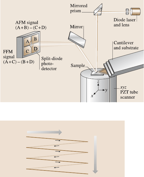
Fig. 21.5. Principles of operation of a commercial small sample AFM/FFM
Fast scan direction Slow scan
direction
Fig. 21.6. Schematic of tri-
angular pattern trajectory of
the AFM tip as the sample is
scanned in two dimensions.
During imaging, data are
recorded only during scans
along the solid scan lines
mode or a square-pyramidal etched single-crystal silicon tip with a rectangular sili-
con cantilever beam (Fig. 21.7) is generally used at normal loads ranging from 10
to 150nN. A preferred method of measuring friction and calibration procedures for
conversionof voltagescorrespondingto normal andfrictionforces to forceunits, are
describedby Bhushan[10,12,13].Thesamples aretypicallyscanned overscan areas
ranging from 50nm×50nm to 10µm×10 µm, in a direction orthogonal to the long
axis of the cantilever beam [14]. The scan rate is on the order of 1Hz. For example,
for this rate, the sample scanningspeed wouldbe 1µm/s for a 500nm×500nm scan
area. Adhesive force measurements are performed in the so-called friction calibra-
tion mode. In this technique, the tip is brought in contact with the sample and then
pulled away. The force required to pull the tip off the sample is a measure of adhe-
sive force.
In nanoscale wear studies, the sample is initially scanned twice, typically at
10nN to obtain the surface profile, then scanned twice at a higher load of typi-
cally 100nN to wear and to image the surface simultaneously, and then rescanned
twice at 10nN to obtain the profile of the worn surface. For magnetic media stud-
ied by Bhushan and Ruan [15], no noticeable change in the roughness profiles was
observed between the initial two scans at 10nN and between profiles scanned at
1144 Bharat Bhushan
5μm
10μm
Square pyramidal silicon nitride tip
Square pyramidal single-crystal silicon tip
Three-sided pyramidal natural diamond tip
2μm
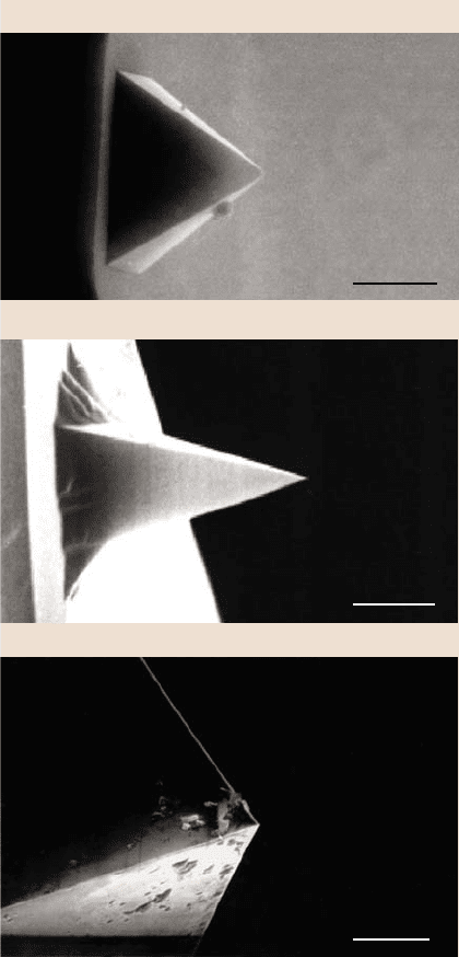
Fig. 21.7. SEM micrographs of a square-pyramidal PECVD Si
3
N
4
tip with a triangular
cantilever beam (top), a square-pyramidal etched single-crystal silicon tip with a rectangu-
lar silicon cantilever beam (middle), and a three-sided pyramidal natural diamond tip with
a square stainless steel cantilever beam (bottom)
21 Micro/Nanotribology and Micro/Nanomechanics of Magnetic Storage Devices 1145
100nN and the final scans at 10nN. Therefore any changes in the topography be-
tween the initial scans at 10nN and the scans at 100nN (or the final scans at 10nN)
are believed to occur as a result of local deformation of the sample surface. In pi-
coindentation studies, the sample is loaded in contact with the tip. During load-
ing, tip deflection (normal force) is measured as a function of vertical position of
the sample. For a rigid sample, the tip deflection and the sample traveling distance
(when the tip and sample come into contact) are equal. Any decrease in the tip de-
flection as compared to vertical position of the sample represents indentation. To
ensure that the curvature in the tip deflection-sample traveling distance curve does
not arise from PZT hysteresis, measurements on several rigid samples, including
single-crystal natural diamond (IIa), were made by Bhushan and Ruan [15]. No cur-
vature was noticed for the case of rigid samples. This suggests that any curvature
for other samples should arise from the indentation of the sample.
For microscale scratching, microscale wear and nanoscale indentation hardness
measurements, a three-sided pyramidal single-crystal natural diamond tip with an
apex angle of 80
◦
and a tip radius of about 100nm (determined by scanning elec-
tronmicroscopyimaging)(Fig. 21.7)is usedat relativelyhigh loads (1µN–150µN).
The diamond tip is mounted on a stainless steel cantilever beam with normal stiff-
ness of about 25N/m [16–19]. For scratching and wear studies, the sample is gen-
erally scanned in a direction orthogonal to the long axis of the cantilever beam
(typically at a rate of 0.5 Hz). For wear studies, typically an area of 2 µm× 2 µm
is scanned at various normal loads (ranging from 1 to 100µN) for selected number
of cycles. Scratching can also be performed at ramped loads [20]. For nanoinden-
tation hardness measurements, the scan size is set to zero and then normal load is
applied to make the indents. During this procedure, the diamond tip is continuously
pressed against the sample surface for about two seconds at various indentation
loads. Sample surface is scanned before and after the scratching, wear, or nanoin-
dentation, to obtain the initial and the final surface topography, at a low normal load
of about 0.3 µN using the same diamond tip. An area larger than the scratched, worn
or indentation region is scanned to observe the scratch, wear scars, or indentation
marks. Nanohardness is calculated by dividing the indentation load by the projected
residual area of the indents [17]. Nanohardness and Young’s modulus of elastic-
ity (stiffness) at shallow depths as low as 5 nm are measured using a depth-sensing
capacitance transducer system in an AFM [19].
Indentation experiments provide a single-point measurement of the Young’s
modulus of elasticity (stiffness), localized surface elasticity as well as phase con-
trast maps (to obtain viscoelastic properties map) can be obtained using dynamic
force microscopy in which an oscillating tip is scanned over the sample surface in
contact under steady and oscillating load [21–24]. Recently, a torsional resonance
(TR) mode has been introduced [25, 26] which provides higher resolution. Stiff-
ness and phase contrast maps can provide magnetic particle/polymer distributions
in magnetic tapes as well as lubricant film thickness distribution.
Boundary lubrication studies are conducted using either Si
3
N
4
or diamond tips
[27–30]. The coefficient of friction is monitored as a function of sliding cycles.
1146 Bharat Bhushan
All measurements are carried out in the ambient atmosphere (22±1
◦
C,
45±5%RH, and Class 10000).
21.2.2 Test Specimens
Data on various head slider materials and magnetic media are presented in the chap-
ter. Al
2
O
3
−
TiC (70–30 w/o) and polycrystalline and single-crystal (110) Mn
−
Zn
ferrite are commonly used for construction of disk and tape heads. Al
2
O
3
, a single-
phasematerial, is alsoselected forcomparisonswith the performanceof Al
2
O
3
−
TiC,
a two-phasematerial. An α-type SiC is also selected which is a candidate slider ma-
terial because of its high thermal conductivity and attractive machining and friction
and wear properties [31]. Single crystal silicon has also been used in some head
sliders but its use is discontinued [32].
Two thin-film rigid disks with polished and textured substrates, with and with-
out a bonded perfluoropolyether are selected. These disks are 95mm in diameter
made of Al
−
Mg alloy substrate (1.3mm thick) with a 10 µm thick electroless plated
Ni
−
P coating, 75 nm thick (Co
79
Pt
14
Ni
7
) magnetic coating, 20nm thick amorphous
carbon or diamondlike carbon (DLC) coating (microhardness ≈ 1,500kg/mm
2
as
measured using a Berkovich indenter), and with or without a top layer of perfluoro-
polyether lubricant with polar end groups (Z-DOL) coating. The thickness of the
lubricant film is about 2 nm. The metal particle (MP) tape is a 12.7mmwideand
13.2µm thick (PET basethicknessof 9.8 µm, magnetic coating of 2.9µm with metal
magnetic particles and nonmagnetic particles of Al
2
O
3
and Cr
2
O
3
, and back coat-
ing of 0.5 µm). The barium ferrite (BaFe) tape is a 12.7mm wide and 11µmthick
(PET base thicknessof 7.3µm, magnetic coating of 2.5 µm with barium ferritemag-
netic particles and nonmagnetic particles of Al
2
O
3
, and back coating of 1.2 µm).
Metal evaporated (ME) tape is a 12.7mm wide tape with 10 µm thick base, 0.2 µm
thick evaporated Co
−
Ni magnetic film and about 10nm thick perfluoropolyether
lubricant and a backcoat. PET film is a biaxially-oriented, semicrystalline polymer
with particulates. Two sizes of nearly spherical particulates are generally used in the
construction of PET: submicron ( ≈ 0.5µm) particles of typically carbon and larger
particles (2–3 µm) of silica.
21.3 Surface Roughness
Solid surfaces, irrespective of the method of formation, contain surface irregulari-
ties or deviations from the prescribed geometrical form. When two nominally flat
surfaces are placed in contact, surface roughness causes contact to occur at discrete
contact points. Deformationoccurs at thesepoints, and maybe eitherelastic or plas-
tic, depending on the nominal stress, surface roughness and material properties.The
sum of the areas of all the contact points constitutes the real area that would be in
contact, and for most materials at normal loads, this will be only a small fraction
of the area of contact if the surfaces were perfectly smooth. In general, real area of
contact must be minimized to minimize adhesion, friction and wear [12].

21 Micro/Nanotribology and Micro/Nanomechanics of Magnetic Storage Devices 1147
Characterizing surface roughness is therefore important for predicting and un-
derstanding the tribological properties of solids in contact. Various measurement
techniques are used to measure surface roughness. The AFM is used to measure
surface roughnesson length scales from nanometers to micrometers.A second tech-
nique is noncontactoptical profiler(NOP) which is a noncontact techniqueand does
not damage the surface. The third technique is stylus profiler (SP) in which a sharp
tip is dragged over the sample surface. These techniques differ in lateral resolution.
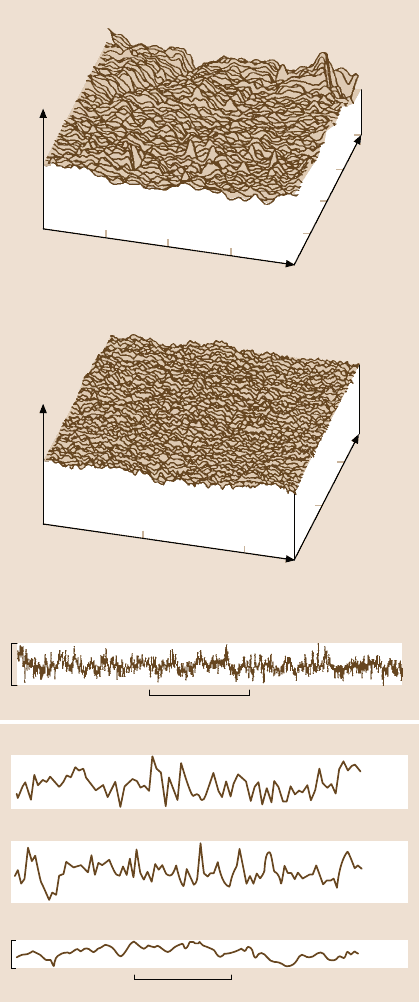
Roughness plots of a glass-ceramic disk measured using an AFM (lateral resolution
≈ 15 nm), NOP (lateral resolution ≈ 1µm) and SP (lateral resolution of ≈ 0.2 µm)
are shown in Fig. 21.8a. Figure 21.8b compares the profiles of the disk obtained
with different instruments at a common scale. The figures show that roughness is
found at scales ranging from millimeter to nanometer scales. Measured roughness
profile is dependent on the lateral and normal resolutions of the measuring instru-
ment [33–37]. Instruments with different lateral resolutions measure features with
different scale lengths. It can be concluded that a surface is composed of a large
number of length of scales of roughness that are superimposed on each other.
Surface roughness is most commonly characterized by the standard deviation
of surface heights which is the square roots of the arithmetic average of squares of
the vertical deviation of a surface profile from its mean plane. Due to the multiscale
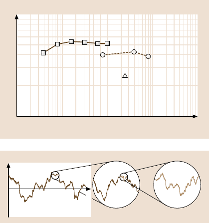
nature of surfaces, it is found that the variances of surface height and its derivatives
and other roughness parameters depend strongly on the resolution of the roughness
measuringinstrument or anyother form of filter, hence not unique for a surface [35–
38] (Fig. 21.9). Therefore, a rough surface should be characterized in a way such
that the structural information of roughness at all scales is retained. It is necessary
to quantify the multiscale nature of surface roughness.
An unique property of rough surfaces is that if a surface is repeatedly magnified,
increasing details of roughness are observed right down to nanoscale. In addition,
the roughnessat all magnifications appear quite similar in structure, as qualitatively
shown in Fig. 21.10. The statistical self-affinity is due to similarity in appearance
of a profile under different magnifications. Such a behavior can be characterized by
fractal analysis [35,39]. The main conclusion from these studies are that a fractal
characterizationof surface roughnessis scale independentand providesinformation
of the roughness structure at all length scales that exhibit the fractal behavior.
Structure function and power spectrum of a self-affine fractal surface follow
a power law and can be written as (Ganti and Bhushan model)
S(τ) = Cη
(
2D−3
)
τ
(
4−2D
)
, (21.1)
P(ω) =
c
1
η
(2D−3)
ω
(
5−2D
)
, (21.2a)
and
c
1
=
Γ
(
5−2D
)
sin[π
(
2−D
)
]
2π
C . (21.2b)
1148 Bharat Bhushan
100
50
0
nm
0
1.00
2.00
3.00
4.00
μm
0
1.00
2.00
3.00
4.00
100
50
0
nm
0
100
μm
0
100
200
200
σ = 4.16 nm R
p
= 18.3 nm
P-V = 39.9 nm
β
*
= 0.20 μm
σ = 2.51 nm R
p
= 5.34 nm
P-V = 10.9 nm
β
*
= 12.6 μm
AFM
NOP
σ = 3.50 nm R
p
= 14.0 nm
P-V = 25.0 nm
β
*
= 4.52 μm
30 nm
500 μm
SP
Fig. 21.8. Surface roughness
plots of a glass-ceramic disk
(a) measured using an atomic
force microscope (lateral res-
olution ≈ 15 nm), noncontact
optical profiler (NOP) (lateral
resolution ≈ 1 µm) and stylus
profiler (SP) with a stylus
tip of 0.2µm radius (lateral
resolution ≈ 0.2 µm), and
(b) measured using an AFM
(≈ 150 nm), SP ( ≈ 0.2 µm),
and NOP (≈ 1 µm) and plot-
ted on a common scale [36]
σ = 4.37 nm, R
p
= 11.3 nm, P-V = 20.3 nm, β
*
= 1.01 μm
AFM
SP
NOP
σ = 4.11 nm, R
p
= 12.0 nm, P-V = 23.1 nm, β
*
= 1.04 μm
σ = 2.18 nm, R
p
= 4.24 nm, P-V = 10.0 nm, β
*
= 6.64μm
30 μm
10 nm
21 Micro/Nanotribology and Micro/Nanomechanics of Magnetic Storage Devices 1149
10
1
σ (nm)
10000
Scan size (μm)
1000100101
AFM
SP
NOP
Fig. 21.9. Scale dependence
of standard deviation of
surface heights for a glass-
ceramic disk, measured using
atomic force microscope
(AFM), stylus profiler (SP),
and noncontact optical pro-
filer (NOP)
z
x
Fig. 21.10. Qualitative de-
scription of statistical self-
affinity for a surface profile
The fractal analysis allows the characterization of surface roughness by two par-
ameters D and C which are instrument-independent and unique for each surface.
D (ranging from 1 to 2 for surface profile) primarily relates to relative power of
the frequency contents and C to the amplitude of all frequencies. η is the lateral
resolution of the measuring instrument, τ is the size of the increment (distance),
and ω is the frequency of the roughness. Note that if S(τ)orP(ω) are plotted as
a function of τ or ω, respectively, on a log-log plot, then the power law behavior
would result into a straight line. The slope of line is related to D and the location of
the spectrum along the power axis is related to C.
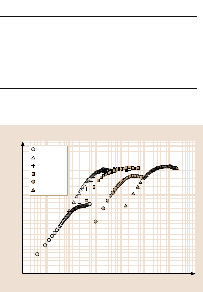
Figure 21.11 present the structure function of a thin-film rigid disk measured
using AFM, non-contactoptical profiler (NOP), and stylus profiler (SP). Horizontal
shiftin thestructurefunctionsfromone scanto another,arises fromthechange inthe
lateral resolution. D and C values for various scan lengths are listed in Table 21.1.
We note that fractal dimension of the various scans is fairly constant (1.26 to 1.33);
however, C increases/decreases monotonically with σ for the AFM data. The error
in estimation of η is believed to be responsible for variation in C. These data show
that the disk surface follows a fractal structure for three decades of length scales.
Majumdarand Bhushan[40] and Bhushanand Majumdar [41] developeda frac-
tal theory of contact between two rough surfaces. This model has been used to
predict whether contacts experience elastic or plastic deformation and to predict
the statistical distribution of contact points. For a review of contact models, see
Bhushan [42,43] and Bhushan and Peng [44].
Based on the fractal model of elastic–plastic contact, whether contacts go
through elastic or plastic deformation is determined by a critical area which is
1150 Bharat Bhushan
Table 21.1. Surface roughness parameters for a polished thin-film rigid disk
Scan size (µm×µm) σ (nm) DC(nm)
1(AFM) 0.7 1.33 9.8×10
−4
10 (AFM) 2.1 1.31 7.6×10
−3
50 (AFM) 4.8 1.26 1.7×10
−2
100 (AFM) 5.6 1.30 1.4×10
−2
250 (NOP) 2.4 1.32 2.7×10
−4
4000 (NOP) 3.7 1.29 7.9×10
−5
AFM – Atomic force microscope,
NOP – Noncontact optical profiler
10
–14
10
–15
10
–16
10
–17
10
–18
10
–19
10
–8
10
–6
10
–4
10
–2
S(τ)(m
2
)
τ (m)
1 μm
10 μm
50 μm
100 μm
250 μm
4000 μm
Fig. 21.11. Structure func-
tions for the roughness data
measured at various scan
sizes using AFM (scan sizes:
1 µm×1 µm, 10 µm×10 µm,
50 µm×50 µm, and 100 µm),
NOP (scan size: 250 µm×
250 µm), and SP (scan length:
4000 µm), for a magnetic
thin-film rigid disk [35]
a function of D, C, hardness and modulus of elasticity of the mating surfaces. If
contact spot is smaller than the critical area, it goes through the plastic deforma-
tions and large spots go through elastic deformations. The critical contact area for
inception of plastic deformation for a thin-film disk was reported by Majumdar and
Bhushan [40] to be about 10
−27
m
2
, so small that all contact spots can be assumed
to be elastic at moderate loads.
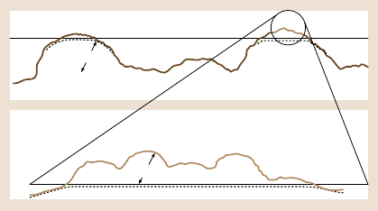
The question remains as to how large spots become elastic when they must have
initially been plastic spots. The possible explanation is shown in Fig. 21.12. As
two surfaces touch, the nanoasperities (detected by AFM type of instruments) first
coming into contact have smaller radii of curvature and are therefore plastically de-
formed instantly, and the contact area increases. When load is increased, nanoasper-
ities in the contact merge, and the load is supported by elastic deformation of the
large scale asperities or microasperities (detected by optical profiler type of instru-
ments) [33].
Majumdar and Bhushan [40] and Bhushan and Majumdar [41] have reported
relationships for cumulative size distribution of the contact spots, portions of the
21 Micro/Nanotribology and Micro/Nanomechanics of Magnetic Storage Devices 1151
200 μm
250 nm
Fig. 21.12. Schematic of local
asperity deformation during
contact of a rough surface,
upper profile measured by
an optical profiler and lower
profile measured by AFM,
typical dimensions are shown
for a polished thin-film rigid
disk against a flat head slider
surface [33]
real area of contact in elastic and plastic deformation modes, and the load-area rela-
tionships.
21.4 Friction and Adhesion
Friction and adhesion of magnetic head sliders and magnetic media have been
measured by Bhushan and Koinkar [16,45–48], Bhushan and Ruan [15], Ruan and
Bhushan [14], Bhushan et al. [27], Bhushan [2,4,10],Koinkar and Bhushan [28,29,
38,49], Kulkarni and Bhushan [50], and Li and Bhushan[51,52], and Sundararajan
and Bhushan [53].
Koinkar and Bhushan[28,29] and Poon and Bhushan[36,37]reported thatRMS
roughness and friction force increase with an increase in scan size at a given scan-
ning velocity and normal force. Therefore, it is important that while reporting fric-
tion force values, scan sizes and scanning velocity should be mentioned. Bhushan
and Sundararajan [54] reported that friction and adhesion forces are a function of
tip radius and relative humidity (also see [29]). Therefore, relative humidity should
be controlled during the experiments. Care also should be taken to ensure that tip
radius does not change during the experiments.
21.4.1 Magnetic Head Materials
Al
2
O
3
−
TiC is a commonly used slider material. In order to study the friction char-
acteristics of this two phase material, friction of Al
2
O
3
−
TiC (70–30wt %) surface
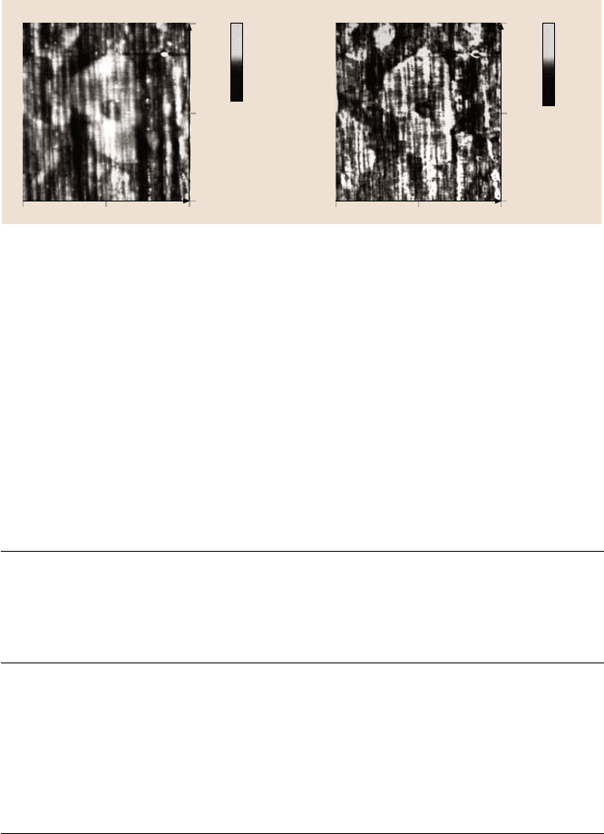
was measured. Figure 21.13 shows the surface roughness and friction force pro-
files [28]. TiC grains havea Knoophardness of about 2800kg/mm
2
which is higher
than that of Al
2
O
3
grains of about 2100kg/mm
2
. Therefore, TiC grains do not pol-
ish as much and result in a slightly higher elevation (about 2–3 nm higher than that
of Al
2
O
3
grains). Based on friction force measurements, TiC grains exhibit higher
friction force than Al
2
O
3
grains.The coefficients of friction of TiCand Al
2
O
3
grains
are 0.034 and 0.026, respectively and the coefficient of friction of Al
2
O
3
−
TiC com-
posite is 0.03. Local variation in friction force also arises from the scratches present
on the Al
2
O
3
−
TiC surface. Thus, local friction values of a two phase materials can
1152 Bharat Bhushan
5.00
2.50
0
0 2.50 5.00
20.0 nm
10.0 nm
0.0 nm
5.00
2.50
0
0 2.50 5.00
50 nN
25 nN
0 nN
Surface height Friction force
μm
μm
Fig. 21.13. Gray scale surface roughness (σ = 0.97 nm) and friction force map (mean =
7.0nN,σ = 0.60 nN) for Al
2
O
3
−
TiC (70 to 30 wt %) at a normal load of 166 nN
be measured. Ruan and Bhushan [55] reported that local variation in the coeffi-
cient of friction of cleaved HOP graphite was significant which arises from struc-
tural changes occurring during the cleaving process. The cleaved HOPG surface
is largely atomically smooth but exhibits line shaped regions in which the coeffi-
cient of friction is more than an order of magnitude larger. These measurements
suggest that friction measurements can be used for structural mapping of the sur-
faces.
Table 21.2. Surface roughness(σ and P–V distance), micro- and macro-scale friction, micro-
scratching/wear, and nano- and microhardness data for various samples
Sample Surface Coefficient of friction Scratch Wear Hardness
roughness depth depth Nano Micro
(1 µm×1 µm) Macroscale
b
at at at 2 mN
σ P− V
a
Micro- Initial Final 60µN60µN(GPa)(GPa)
(nm) (nm) scale (nm) (nm)
Al
2
O
3
0.97 9.9 0.03 0.18 0.2–0.6 3.2 3.7 24.8 15.0
Al
2
O
3
−
TiC 0.80 9.1 0.05 0.24 0.2–0.6 2.8 22.0 23.6 20.2
Polycrystalline 2.4 20.0 0.04 0.27 0.24–0.4 9.6 83.6 9.6 5.6
Mn
−
Zn ferrite
Single- 1.9 13.7 0.02 0.16 0.18–0.24 9.0 56.0 9.8 5.6
crystal (110)
Mn
−
Zn ferrite
SiC (α-type) 0.91 7.2 0.02 0.29 0.18–0.24 0.4 7.7 26.7 21.8
a
Peak-to-valley distance
b
Obtained using silicon nitride ball with 3 mm diameter in a reciprocating mode at a normal
load of 10 mN, reciprocating amplitude of 7 mm and average sliding speed of 1 mm/s. Initial
coefficient of friction values were obtained at first cycle (0.007 m sliding distance) and final
values at a sliding distance of 5 m
