Baca A.G., Ashby C.I.H. Fabrication of GaAs Devices
Подождите немного. Документ загружается.


Ohmic contacts
conduction band in the bulk of the semiconductor. The bending of
the conduction band at the metal/semiconductor interface sets the
barrier to current flow across the interface, as in FIGURE 6.3.
Electrons may cross the potential or Schottky barrier by one of
two mechanisms: thermionic emission or field emission (tunnel-
ling). A combination of the two mechanisms is termed thermionic-
field emission. In thermionic emission, a fraction of the electrons
have sufficient thermal energy to cross the barrier. The fraction is
related to the factor
exp(−qφ
b
/kT) (6.4)
and the current due to thermionic emission is given by
J = (const) exp(−qφ
b
/kT)[exp(qV/nkT) − 1]
J = J
s
[exp(qV/nkT) − 1]
(6.5)
where φ
b
is the barrier height, q is the electron charge, k is
Boltzmann’s constant, V is the applied voltage across the bar-
rier and n is the ideality factor (discussed in Section 7.2.1). The
purpose of an ohmic contact is to provide a low-resistance con-
tact. EQN (6.5) indicates that low currents arise with low voltages
unless the Schottky barrier is fairly low.
The second mechanism for current flow across a barrier, field
emission, allows for quantum mechanical-tunnelling through
the Schottky barrier. The equation governing current from field
emission is given by
J = exp(−qφ
b
/E
00
) (6.6)
where
E
00
= qh (N/εm
∗
)
1/2
/2 (6.7)
and h
is Planck’s constant dividedby2π, ε is the dielectric constant,
N is the doping concentration and m
∗
is the electron effective mass.
Field emission works by electrons tunnelling through the Schottky
barrier, whose width is roughly the same as the thickness of the
depletion region. The tunnelling current increases exponentially
with the doping concentration. Practically speaking, this current
becomes significant enough to make low resistance contacts to
GaAs when N exceeds 10
19
cm
−3
.
In reality, both thermionic and field emission can come into play
for contacts at room temperature. This type of conduction is termed
thermionic field emission and it works by electron tunnelling from
thermally excited electrons that tunnel through a somewhat thinner
barrier by virtue of the electron energy being somewhat higher than
the Fermi level.
182
Ohmic contacts
As seen from EQNS (6.5)–(6.7), lowering the barrier height and
increasing the doping concentration are the two basic means for
creating an ohmic contact to any semiconductor. Simple as this
seems, GaAs presents a somewhat difficult case for barrier height
lowering. Surface or interface state densities are fairly high for
GaAs, compared with the SiO
2
/Si interface, for example, which
has the practical effect of pinning the Fermi level to midgap and
constraining the barrier heights of most metal/GaAs contacts to
a fairly narrow range (Section 7.4). If barrier-height-lowering is
to be a practical method, the creation of lower bandgap materials or
the creation of lower-barrier-height interfaces are the only avail-
able approaches. Some metallurgical approaches along this line
will be presented in the next section. Alternatively, the strategy
for designing an ohmic contact can rely on achieving high doping
levels.
6.2.3 Metallurgy of ohmic contact formation
Although Ge/Au/Ni is the dominant contact metallurgy for n-type
GaAs, literally hundreds of recipes exist for ohmic contact forma-
tion to GaAs and no mechanism is expectedtoexplain all thedetails
of the various ohmic contact processes. It is somewhat surprising,
therefore, that most of the contacts to GaAs seem to follow the
broad outlines of a general mechanism. Studying this mechanism
can help the practising engineer understand the importance of the
various elements of the recipe and relate them to the otherwise con-
fusing folklore that is sometimes told about GaAs contacts. Prior
to a description of this mechanism, a few historical highlights of
GaAs ohmic contacts will be presented.
Some folklore about GaAs contacts
(and reply). See text for more
mechanistic explanation.
AuGe eutectic: Eutectic chosen so that
contacts will melt at chosen
temperature; molten alloy allows Ge to
diffuse better into GaAs.
Reply: The mechanisms for Ge and
other constituents to diffuse into GaAs
can work well at temperatures well
below the eutectic melting of GeAu.
Role of Ge: Ge acts as n-type dopant
in GaAs.
Reply: Ge reactions with Ni are also
important.
Role of Ni: Ni acts as a wetting agent so
that the melted AuGe will not “ball up.”
Reply: Ni plays an important role at
temperatures well below the AuGe
eutectic.
Sn was used as an early contact to GaAs, while GeAuNi became
the most widely used contact after its report in 1967 [1]. Inter-
estingly, Ge and Au were used in their eutectic composition,
88% Au and 12% Ge by weight, which is the composition of low-
est melting point. Metal alloys with eutectic compositions have
many uses, including the attachment of semiconductor chips to
their package by eutectic melting and bonding. Ohmic contacts
with low-bandgap surface regions obtained by epitaxial growth
of InGaAs were first reported in 1981 [2] and many variations
on this theme were later reported. Contacts based on solid-state
regrowth using the Pd/Ge metal system were introduced in 1985 as
a way of improving the reliability of ohmic contacts by understand-
ing and controlling their metallurgical reactions [3]. Although
these contacts were never widely adopted, the subsequent research
on solid-state regrowth solidified our understanding of basic
mechanisms in contact formation.
The metallurgy of ohmic contact formation to n-type GaAs will
include some or all of the following steps: 1) an element of the
183
Ohmic contacts
contact reacts with the native oxide present on the GaAs surface,
2) a low temperature process occurs where one element of the con-
tact, the Ni in Ge/Au/Ni alloys, diffuses into GaAs and reacts to
form intermediate X-GaAs complexes, “decomposing” the GaAs
or otherwise facilitating interdiffusion between the contact and
GaAs, 3) an element of the contact capable of doping GaAs diffuses
into the GaAs aided by defects created in step 2 and dopes GaAs,
4) an element of the contact capable of forming a low bandgap
alloy with GaAs diffuses into the GaAs, 5) Ga outdiffuses from
GaAs and reacts with a contact element, often Au, 6) elements
of the contact continue to react and form their thermodynamically
favoured alloys until the reaction is complete or the thermal budget
is exhausted, 7) excess As diffuses to the surface where it resides
or vapourises.
The most commonly used contact is GaAs/Ge/Au/Ni. The
metallurgy of this contact probably includes six of the steps out-
lined above. The Ge/Au/Ni contact will be described in terms of
these steps of the metallurgy as a specific example of the reactions.
In step 1, the Ni reacts with the native oxide. The native oxide is
not easily characterised on GaAs and may vary in unrepeatable
ways due to variations in processing, so it is useful for the contact
to have a constituent such as Ni that will reliably react with differ-
ent types of surface oxide. GeAu contacts without Ni are known
to have poor morphology and large variability. The native oxide of
GaAs may have regions that allow easy penetration of the GeAu
and the alloy formation occurs rapidly in these areas. Other areas
may never react because the GeAu does not penetrate the native
oxide and poor morphology results.
Summary: 7 common steps of GaAs
ohmic contact alloy reactions
1. An element of the contact reacts
with the GaAs native oxide.
2. An element of the contact reacts
with GaAs at low temperatures to
form a X-GaAs complex.
3. An element of the contact diffuses
into GaAs mediated by defects
created in step 2 and dopes GaAs.
4. An element of the contact diffuses
into GaAs and forms a low bandgap
semiconductor phase.
5. Ga outdiffuses from the contact and
reacts, usually with Au.
6. Elements of the contact react and
form their thermodynamically
preferred compounds.
7. As diffuses from the GaAs to the
contact surface where it resides or
vaporises.
In step 2, the Ni forms intermediate complexes with GaAs. The
Ni-GaAs complexes later give way to more stable products such
as AuGa intermetallic reaction products. The important role of the
intermediate complexes is to disturb the crystal lattice to make way
for diffusion of other atoms and further reactions. In the case of
GeAuNi contacts, the absence of Ni would result in more thermal
energy required for the Au and Ge reactions to get started. Once
started they quickly get out of control leading to severe spiking and
poor morphology. The Ni-based complexes are thought to form at
temperatures below 100
◦
C.
Once the Ni-GaAs complexes have disturbed the crystal lattice,
the way is prepared for the diffusion of Ge into the GaAs in
step 3. Normally, diffusion of dopants such as Ge in GaAs requires
a substitutional-interstitial mechanism where the Ge can diffuse
along interstitial sites until it finds a vacancy in the GaAs lattice.
This type of mechanism has high activation energy and normally
occurs to a significant degree at temperatures of 600
◦
C and above.
In a GaAs ohmic contact, the diffusion process is thought to occur
184
Ohmic contacts
at much lower temperatures because of the driving forces of the
Ni-GaAs complex formation and the driving force of the next
reaction which further disturbs the crystal lattice. The high activ-
ation energies of creating and filling Ga vacancies are overcome
by complex reaction intermediates involving Ni-Ge-GaAs rather
than by thermal effects that are necessary during substitutional-
interstitial diffusion. The diffusion of Ge into GaAs at tem-
peratures between 100 and 400
◦
C leads to very high doping
levels that make tunnelling contacts possible for doping levels
above 10
19
.
It is not presently believed that ohmic contact formation with
Ge/Au/Ni in GaAs participates in step 4 through the formation of
a low bandgap alloy, though NiAs phases were considered pos-
sible low-barrier-height phases in the past. The second part of
the driving force for steps 2 and 3 comes from a step 5 reaction,
the Au-Ga reaction. The Au-Ga alloy is more thermodynamically
stable than any other compound between the five elements that
can form. At temperatures at and above 250
◦
C, this reaction is
kinetically favoured and with sufficient time will continue until
the supply of Au is exhausted.
In step 6, other reactions between the GaAs and the contact
constituents continue. Some of these reactions form intermediate
compounds such as NiAs while others such as NiGe are more
stable.
The last step is the transport of As to the surface of the con-
tact and its desorption from the contact. Among the five reacting
elements, As is most stable in the elemental phase and leaves the
GaAs. The significance of this step along with step 5 is the con-
sumption of GaAs. Voids formed by the loss of As are formed
and filled with AuGa, NiGe and other stable compounds. In the
ideal case with good processing technique, the reaction occurs
uniformly. Because the ideal case is usually only approximately
achieved and because the reactions occur very fast, spikes form
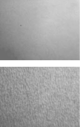
if there are any process non-uniformities. Visual inspection of an
alloyed GaAs/Ge/Au/Ni contact will show a textured surface for
a properly alloyed contact (FIGURE 6.4(a)) and a much greater
morphology change for over-alloyed contacts (FIGURE 6.4(b)).
Surface profilometry or atomic force microscopy measurements
will show depressions in the areas where the contact has spiked
and excess As has been consumed. Transmission electron micro-
scopy directly images the regions where spiking has occurred and
has been used to identify some of the reaction products.
(a)
(b)
FIGURE 6.4 Optical micrograph
of an alloyed GeAuNi ohmic
contact: a) slight texture for
properly alloyed contact, b) greater
texture for over-alloyed contact.
Most contact metallurgies in use today follow some of the seven
steps outlined in this section. Some of these steps have resulted in
problematic characteristics for a GaAs ohmic contact and have
stimulated further research. Much of the research has resulted
185
Ohmic contacts
in optimisation and better understanding of the mechanism of
the GaAs/Ge/Au/Ni contact. Some alternative metallurgies have
been developed and the more common ones will be reviewed in
Section 6.3.
(a)
(b)
(c)
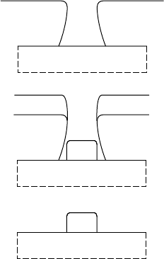
FIGURE 6.5 Illustration of the
steps required for forming an
ohmic contact.
6.3 FABRICATION AND TESTING OF
OHMIC CONTACTS
6.3.1 Fabrication of ohmic contacts
The fabrication of an ohmic contact involves the steps of pattern-
ing the GaAs with resist or another suitable mask, preparing or
cleaning the surface, depositing the metal, and alloying the metal,
if needed. The most common process is to pattern the sample first
and to use a liftoff process to produce the patterned contact. The
basic steps are illustrated in FIGURE 6.5. A photoresist is applied
to the wafer and spun typically between 1500 and 6000 rpm to
uniformly coat the wafer. The resist thickness should be uniform
so that good control of the final linewidth can be achieved. Photo-
lithography is discussed in greater detail in Chapter 4. A glass or
quartz mask is then aligned to the pattern on the wafer so that light
can pass through the areas to be exposed and be blocked in the areas
to be protected from the light. Any of the available lithography
tools may be used, but the optical stepper is the tool of choice
for most high-performance and high-yield processes in HBT and
FET fabrication. Once the mask is aligned with the wafer, the res-
ist can be exposed to the light and the pattern can be developed
(FIGURE 6.5(a)). A re-entrant cross-sectional profile is desired so
that the surface of the resist shadows the sidewalls and prevents
the evaporated metal from coating them. Re-entrant profiles can be
achieved with either positive or negative (image reversal) resists
(Section 4.4.1). The choice of resists depends on the type of optical
aligner used, the wavelength of the light and factors relating to the
device morphology.
Prior to depositing the ohmic contact, a surface treatment may
be used. This may include a plasma oxygen treatment to remove
monolayers or less of organic material that remain after the resist
develop process. The surface treatment may also include oxide
removal or other steps. The ohmic metal is then evaporated over
the whole wafer where it forms the contacts in the patterned areas
and covers the resist over the rest of the wafer (FIGURE 6.5(b)).
The unwanted metal is removed from the wafer when the resist
is dissolved, typically by means of a solvent spray. At this point,
the ohmic metal (FIGURE 6.5(c)) can be tested electrically if a
non-alloyed ohmic contact process was employed. Otherwise, the
186
Ohmic contacts
contact will be alloyed so that the metallurgical reactions needed
for ohmic contact formation can proceed.
Surface treatments for removing native
oxides of GaAs were described in
Section 3.2.2.
The preceding description is an overview of the fabrication pro-
cess. Several of the fabrication critical steps will now be described
in more detail. The pre-clean step can be critical for achieving
low electrical resistance in the contact. One common procedure
used with Ge/Au/Ni contacts employs a plasma oxygen clean fol-
lowed by an oxide removal step. The GaAs native oxide is about
1–2 nm thick. Exposure of a clean GaAs surface to the ambient
results in the formation of a consistent native oxide. This native
oxide is easily removed by dilute acids such as HF or HCl or bases
such as an NH
4
OH:H
2
O mixture (Section 3.2.2). During routine
semiconductor processing the GaAs comes into contact with other
chemicals such as hydrocarbons in a photoresist formulation that
may leave residues on the surface of the GaAs. In such cases, both
the formation of the native oxide and the reaction of a deposited
ohmic metal are complicated by the presence of hydrocarbon or
ionic residues. It is found that ohmic contacts can have excel-
lent electrical characteristics but are not repeatable. Consequently,
various attempts have been made to improve the repeatability of
ohmic contacts. Several of these involve methods to remove the
hydrocarbon residues.
A common procedure to accomplish the hydrocarbon removal is
to expose the patterned GaAs wafer to an oxygen plasma. Typic-
ally RF radiation at 13.56 MHz is used to create a plasma with
O
2
and maybe a carrier gas such as Ar. Equipment specific-
ally designed for this purpose is often available and one type is
commonly referred to as an “asher”. A popular geometry is the cyl-
indrical shape with a powered metal cylinder enclosing an interior
region that contains the plasma and the samples, which mount to
grounded rods that are placed at positioned breaks in the powered
electrode design. The operation of a barrel asher was described
in Section 5.6 and FIGURE 5.4. This particular design is useful
for hydrocarbon residue removal because the geometry leads to
a lower plasma sheath voltage than the parallel electrode design.
Such a lower self-biasing of the plasma is important for a gen-
eral purpose plasma oxygen process because it is potentially used
multiple times in a typical device fabrication and some of the steps
will have requirements of low or no plasma damage.
A newer method of hydrocarbon removal uses UV-generated
ozone exposure. Ozone can react with hydrocarbon residues by
releasing molecular oxygen and an oxygen radical that quickly
reacts with the hydrocarbon to form carbon oxides and other
organic molecules such as alcohols and ketones. The reactive
ozone is a neutral molecule which forms in the absence of a plasma
and cannot cause the types of damage caused by the acceleration of
187
Ohmic contacts
charged particles. It is therefore ideally suited as a general purpose
hydrocarbon removal tool. Commercial ozonation tools are among
the least complex clean room equipment in that they only need a
source of electrical power. In contrast to ashers, which are designed
to remove several microns of photoresist per hour, ozonators typic-
ally remove resist at a rate of several monolayers per minute. They
are especially valuable for stubborn submonolayer hydrocarbon
removal.
The removal of hydrocarbon residues prior to ohmic contact
deposition is a good way to ensure repeatability of the surface
condition. In addition to removing hydrocarbon deposits that can
block interface reactions, it also can create repeatable conditions
for oxidising the GaAs surface. Although oxides themselves are
potential impediments to interface reactions between the GaAs
and the ohmic contact, they are easily removed prior to contact
deposition and only partially regrow if samples are loaded within
minutes (up to ten is a reasonable compromise between unrealistic-
ally short times and times long enough to fully regrow the oxide) to
the deposition system. Common methods of native oxide removal
by acids such as HCl and HF or bases such as NH
4
OH also work
for the plasma or UV-ozone oxides. A further benefit of incorpor-
ating an oxide removal step in the ohmic contact process is that any
low-level impurities that settle on the GaAs surface are dissolved
with the oxide.
Following the surface preparation methods comes the actual
contact deposition. Evaporation is the technique of choice for most
metal depositions on GaAs because it provides a method of high
purity deposition with minimal damage to the GaAs. This is espe-
cially so for Au-based contacts because an evaporation process
with liftoff patterning works well with Au, while etch processes
are limited to ion milling. Evaporation is carried out in a high-
vacuum chamber with pressure in the mid to low 10
−7
torr pressure
range. This pressure level is required so that the residual gases
in the vacuum chamber will not be a source of contamination
as the deposition proceeds. As previously noted, electron beam
evaporation results in minimal damage to most semiconductors
compared to the main alternative, sputtering. With electron-beam
deposition, no energetic ions are produced which can be accel-
erated to the sample surface and cause lattice damage. The main
concern for damage with electron-beam deposition is the effect
of energetic electrons. For cases where this type of damage is a
concern, thermal evaporation is used. For GaAs ohmic contacts,
lattice damage is not usually a concern because lattice disruption
is an intended consequence of the contact reaction.
A variety of evaporation equipment is available depending on
the degree of throughput and automation needed. For high-volume
188
Ohmic contacts
production, extremely large evaporators are available with the
capability of depositing on dozens of wafers per run. These large
vacuum systems are equipped with heavy duty vacuum pumps that
can bring about the required vacuum conditions in considerably
less than 1 h. On the other end of the spectrum, research tools have
much smaller vacuum chambers and pumps and may require sev-
eral hours for pump down after sample loading. A brief description
of the steps in an electron beam deposition follows.
An electron beam typically accelerated to 10 kV is directed at
one of the hearths or crucibles containing the high-purity solid.
The energetic electrons enter the solid where collisions and scat-
tering events with valence and core electrons from the solid result
in energy transfer from the accelerated electron to the solid source.
Ultimately, the source heats up in the localised area where the elec-
tron beam is focused and begins to melt and evaporate. It becomes
a source of atomic flux throughout the chamber. The acoustic wave
properties of a quartz crystal are used as a flux monitor to provide
feedback to the electron beam source and to stabilise the flux to a
preset value. Once the flux is stable, a shutter is opened to allow the
sample to receive a thin film deposition. The process is ended when
the desired film thickness is reached and is then repeated for any
other depositions that are needed in a multimetal stack. A thermal
evaporation follows a similar procedure, except that instead of an
electron beam being used to heat up the source material, electrical
current is passed through a refractory metal holder that contains a
small amount of the source material.
The various components of the ohmic contact are typically
deposited layer by layer. For example, deposition of a Ge/Au/Ni
ohmic contact will proceed with the deposition of the Ge layer
first, followed by the Au layer, and finish with the deposition of
the Ni layer. On occasion two constituents will be co-deposited.
This occurs frequently with Au and Ge due to the fact that an alloy
of 12% by weight of Ge and 88% of Au forms the eutectic com-
position and melts at a lower temperature (361
◦
C) than other alloy
compositions. After deposition is completed the shutter is closed
and the evaporator is vented for sample removal.
Source material deposition is completed by the removal of the
resist material and the unwanted metal through a liftoff process. At
this point the contact formation is completed by means of a thermal
annealing step, if required. This step is often termed an ohmic alloy
for contacts that undergo an alloy process. For Ge/Au/Ni contacts
the thermal anneal is typically carried out near 400
◦
C for 10 s to
several minutes. Usually the shorter times require slightly higher
temperatures than the longer times.
A rapid thermal annealer (RTA) is commonly used for this
step, although furnaces and strip heaters are also used. An RTA
189
Ohmic contacts
is composed of several necessary components such as an inert
chamber (often quartz) which will contain the samples, a heater
such as an infrared lamp, a network of plumbing for inert gas
introduction and pumping, and a control system. It is important to
exclude oxygen during the anneal. Oxygen can cause several dele-
terious effects. First, it can oxidise the exposed GaAs surfaces.
Because this oxidation will be occurring at elevated temperat-
ures, the As-oxides are volatile and the process can continue to
the point of consuming a considerable amount of As from the
GaAs. Second, oxygen can react with the contact materials. For the
Ge/Au/Ni ohmic contact, Ge and Ni oxides would seriously inhibit
the intended reactions. The chamber containing the samples is usu-
ally purged with a high purity inert gas to drive out the oxygen.
Some equipment is designed for pump and purge cycles to speed
up this process while other equipment is designed for vacuum
annealing.
Other considerations also come into play for the RTA pro-
cess. One of these is the method of sample placement, which
will affect the thermal loading. One common type of annealer
uses a Si wafer mounted to quartz rods attached to the door of
the chamber with a thermocouple embedded in the wafer. In
such an arrangement, the sample is mounted directly on top of
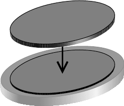
the Si wafer. Another method involves placing the sample in a
specially designed susceptor, as illustrated in FIGURE 6.6. An
example of a sample susceptor for RTA is a SiC disk that is
coated with graphite for chemical inertness and as a radiation
absorbing film. A central circular area is recessed a distance
slightly deeper than the typical sample thickness and is the region
where the sample will be placed. A second disk with a matched
diameter to the recessed region acts as a cover to the sample. This
type of sample arrangement adds thermal loading to the sample
and more uniformity to the temperature profile, and makes for
a more accurate temperature calibration. However, this method
is less amenable to automated handling of the wafers and may
be disadvantageous in production environments that require high
throughput.
FIGURE 6.6 Illustration of a
sample susceptor for an RTA.
Another consideration relates to the efficiency of the heating
process. To reach 400
◦
C, the lamps do not require very much
power and will emit more infrared than visible radiation, much
of it below the GaAs bandgap and not efficiently absorbed by
GaAs. However, the metals in the ohmic metal do absorb the
infrared radiation effectively. In such a situation, the temperat-
ure calibration becomes difficult to achieve, as one must take into
account the quantity and type of thin film deposited on the wafer.
Obviously, the results can be ohmic-pattern dependent. Because
of the difficulty of accounting for the pattern in the temperature
190
Ohmic contacts
calibration, the second type of sample placement within an IR
absorbing susceptor is often preferable.
6.3.2 Measurements of ohmic contacts
The purpose of an ohmic contact is to provide a linear relationship
between current and applied voltage in a semiconductor device. It
is usually desirable to have low access resistance from the device to
the outside world. Consequently the measurement of ohmic con-
tacts to accurately determine their small but finite resistance is an
important part of semiconductor engineering and one which can be
the subject of detailed treatments. For the purpose of this chapter,
only two practical methods of measurement will be introduced.
More detailed treatment of other methods and other models can be
found in [4]. Both methods treated in this chapter will be based on
the planar contact common to FETs and the base and collector of
HBTs. The two methods differ in the test structure chosen, either
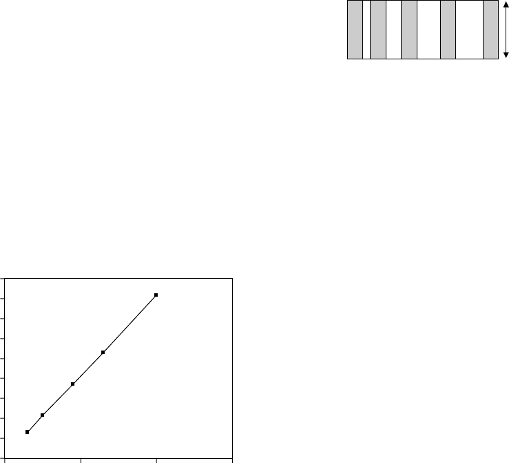
a linear contact array or a circular contact test structure.
w
L
1
L
2
L
3
L
4
FIGURE 6.7 Illustration of
linear contact array.
From a linear contact array illustrated in FIGURE 6.7 with
resistances defined in FIGURE 6.2, the contact resistance R
c
is
given by
R = 2R
c
+ R
sh
L/w (6.8)
where R
sh
is the sheet resistance of the semiconductor between the
contacts, L is the length between the contacts and w is the width
of the contacts. In practice, the linear array contains contact pairs
with differing separations. The resistance of a contact pair is meas-
ured and plotted as a function of L, as illustrated in FIGURE 6.8
for a contact width of 100 μm. The slope of the resistance gives the
sheet resistance (201 /square after normalising length/width of
y = 2.0082x+0.5585
R
2
=0.9998
0
5
10
15
20
25
30
35
40
45
0102030
contact spacin
g
(
mm
)
resistance (
Ω
)
FIGURE 6.8 Plot of resistance versus contact separation to extract contact
resistance.
191