Baca A.G., Ashby C.I.H. Fabrication of GaAs Devices
Подождите немного. Документ загружается.

Dry etching of GaAs and related alloys
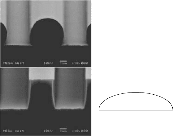
thick reflowed resist thin reflowed resist
FIGURE 5.13 Reflowed resist profiles.
for many Novolac resists and between 140 and 160
◦
C for
4-polyhydroxystyrene (PHS). White light exposurehas been found
to reduce the glass-transition temperature of resist, so perform-
ing all resist handling under yellow lighting is advisable. The T
g
for a particular resist is available from the resist manufacturer.
When a resist exceeds T
g
, it begins to flow to reduce its total sur-
face energy by assuming a curved surface (FIGURE 5.13). While
this phenomenon can be harnessed to controllably etch angled
facets into GaAs by performing the reflow before beginning to
etch, it can be a serious problem if it occurs unintentionally during
an etching process because an angled profile may result when a
vertical one was desired. The horizontal extent of the resist tends
to remain constant, but the volume redistributes into an arched
or even nearly spherical resist profile, depending on the initial
height-to-width ratio.
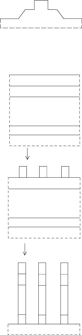
Deliberate variation in the thickness of the resist can be used to
advantage to achieve angled sidewalls with processes that other-
wise produce vertical profiles. This may be especially desirable for
a continuous connection between a metal contact on a mesa ledge
with a metal bond pad on the adjacent wafer surface. To achieve
this effect, the photoresist is first exposed and developed. It is then
heated slightly above its glass transition temperature to induce
some flow. The resist assumes a curved profile to minimise its
surface energy. Controlled erosion of the resist as the wafer etches
gradually exposes the underlying wafer regions, which then etch
172
Dry etching of GaAs and related alloys
to produce the desired angled structures. The type of profile that
results from a two-step etch using first a straight-wall photores-
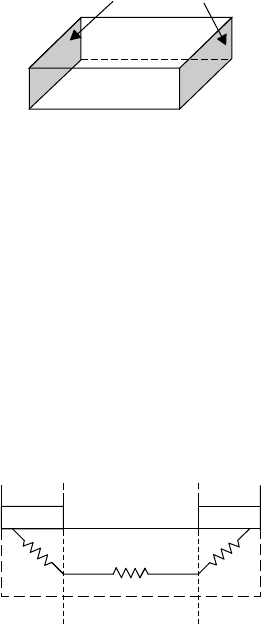
ist and then a reflowed photoresist is shown in FIGURE 5.14.
The angled wall of the second mesa allows good metal contacts to
be made from the top of the angle-walled mesa to bond pads on
the lower etched surface.
FIGURE 5.14 Angled-wall
double mesa structure from
two-step etch with first
straight-wall resist and then
reflowed resist.
To avoid thermal problems for longer etches, one or more
cool-down steps may be included during the etch process. With
source gases that require plasma dissociation to produce appre-
ciable etching, this can simply involve stopping the plasma
discharge while the gases continue to flow for a few minutes.
A good starting time for determining what is required for adequate
cooling is about 5 min. The final etch depth and profile will be
largely determined by the time the plasma is on. For gases that
can do appreciable etching without plasma activation, such a cool-
down step might allow an undesirable amount of isotropic etching,
resulting in degraded profiles.
The required thickness of a resist, especially a metal resist, will
be defined largely by its sputtering rate. Metal resists or multilayer
photoresist/dielectric resist stacks are used in processes such as
RIBE for deep, narrow features where conventional photoresist
cannot withstand the prolonged high-energy etching required.
One solution to the problem of excessively rapid photoresist
erosion is the use of PR/dielectric stacks as trilevel or quadlevel
resists. A quadlevel resist that works well for RIBE andICP etching
is shown in FIGURE 5.15. An organic liftoff layer, such as poly-
methylglutarimide (PMGI), is applied to the substrate. The main
PR mask layer is then applied to the PMGI and extensively baked
(60 min at 190
◦
C followed by 60 min at 250
◦
C). A half micro-
metre of a dielectric such as Si
x
N
y
is applied to this hard-baked
PR. Another PR layer that is used for patterning the dielectric is
applied on top of the stack.
substrate
lift-off layer
hard-baked resist
dielectric
imaging resist
substrate
photolithography
substrate
lift-off layer
hard-baked resist
dielectric
oxygen plasma
(a)
(b)
(c)
FIGURE 5.15 Quad-level mask.
The desired pattern is photolithographically defined in the top
PR layer. This pattern is then etched into the Si
x
N
y
using an SF
6
/O
2
RIE process. The pattern is then transferred into the hard-baked PR
and liftoff layer using an ECR or ICP etch with O
2
and Ar. Fol-
lowing the completion of etching the III–V substrate (typically by
RIBE), what remains of the resist stack can be removed by soaking
in a solvent that releases the liftoff layer from the surface.
Nickel is often a good choice for a metal resist due to its
relatively high resistance to sputtering and its tendency not to
redeposit on the wafer surface when it is sputtered. Redepos-
ition of sputtered material, either resist or low-volatility III–V
products, can produce micromasking. The result is very rough
etching, producing a “grassy” surface that often looks black or
“burned” upon inspection.
173
Dry etching of GaAs and related alloys
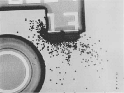
FIGURE 5.16 Effect of sputtered Au micromasking.
When a device wafer is being subjected to more than one etch
process with metallisation being applied between the etch steps,
one must be especially careful to cover the metal with photoresist
to avoid sputtering and redeposition of the metal onto adjacent sur-
faces. This is particularly true for Au-based metallisations. When
Au is sputtered onto the nearby GaAs surfaces, it serves as a micro-
mask and destroys the smooth surface that is generally obtained
in dry etching (FIGURE 5.16). Careful attention to covering all
exposed Au is essential to avoid ruining the device wafer due to
this effect.
5.10.4 Advantages of Ar addition
Argon addition makes it easier to strike a plasma and therefore
extends somewhat the range of gas mixtures, pressures and RF
power that can be employed in RIE. It increases the sputtering
component of any gas mixture, which increases the anisotropy and
often serves to increase the smoothness of a slightly roughening
etch, especially if micromasking is involved. Its optical emission
can also serve as a calibration for semiquantitative applications
of optical emission as a plasma diagnostic. These advantages of
Ar addition apply in both RIE and HDPE processes. Addition
of a few percent Ar can be sufficient to achieve most of these
improvements.
5.10.5 Methods for end-point determination
The simplest method for determining the end point is to etch
for a specific time assuming a known etch rate. While this is
often the only available method, it is not a very reliable one.
Day-to-day variation in the chamber wall conditions can lead to
174
Dry etching of GaAs and related alloys
70
30
60
40
50
50
70
30
60
40
50
50
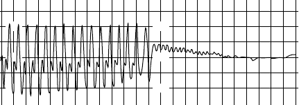
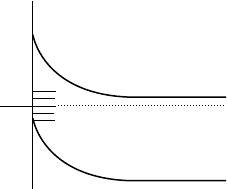
FIGURE 5.17 Optical reflectance spectrum showing the transitions between
different heterolayers.
sufficiently different etch rates that variations in excess of 10% are
routinely encountered. This is especially true when the etch sys-
tem cannot be dedicated to a single process or single wafer layout.
Even variations in the ratio of exposed GaAs to resist can produce
significant rate variations in a dedicated system.
A better method for determining end point while etching het-
erostructures relies on the difference in optical reflectance from
GaAs and III–V ternaries. Optical reflectance of a collimated light
source, such as a laser, is monitored continuously. The resulting
oscillations (FIGURE 5.17) indicate the passage of the etch front
through the heterointerfaces. The physics of this is well understood
and straightforward to model [4]. Modelling is not necessary to
use this technique, however. By simply counting the oscillations,
it is possible to determine when one reaches the specific inter-
face where etching is to stop. If etching needs to proceed into the
underlying GaAs substrate, where no interface oscillations will be
observed, one can still obtain better etch control by calculating
the etch rate through the heterostructure under current chamber
conditions and timing the etch assuming that rate.
If an etch is roughening the wafer, this technique will give
advance warning that it is occurring. As the surface begins to
roughen, the amplitudes of the oscillations are damped. When
damping is first observed to be starting, it is sometimes possible
to “rescue” a sample before it is totally destroyed by the etch
process, correct the source of roughening and try again. Thereflect-
ance spectrum of the aborted run provides information regarding
the depth at which the process was stopped and allows one to
resume monitoring the etch process during the second attempt.
There are some limitations to this technique. Although optical
reflectance can reveal when the desired depth has been achieved
at the point being measured, etch-rate uniformity across the wafer
can lead to a variation in etch depths. In addition, the beam must
be centred on exposed GaAs instead of resist. This can be diffi-
cult with wafers with a high ratio of resist to exposed GaAs (low
exposed fraction of the GaAs surface). Longer-period oscillations
175
Dry etching of GaAs and related alloys
due to the slower erosion of resist will be observed and can
dominate the signal when there is little exposed GaAs.
5.10.6 Plasma diagnostics for trouble-shooting
While a tremendous amount of information about the chemical
species in a plasma can be gleaned from optical emission spectro-
scopy (OES), interpretation of the spectra often requires time and
expertise beyond that of the normal etch system operator. Quant-
itative interpretation of OES requires knowledge of the electron
energy distribution function, the relative excitation cross-sections
for the various plasma species at the range of energies present
in the system, the interspecies relaxation processes and the indi-
vidual emission spectra of the different excited-state species. In
addition, typically less than 5% of the species in a plasma are
in an excited state capable of emitting light, so the majority of
the species that may be contributing to the etch process are not
interrogated by OES.
There are, however, some relatively simple situations in which
optical emission spectra can be extremely useful in identifying
the source of an etching problem. The most significant of these is
the identification of the presence of a leak in the system. While
Cl-based plasmas appear violet, the presence of oxygen from a
moderate leak will change the dominant colour to blue. Oxygen has
characteristic emission peaks at 777.4 nm for O atoms and 486.0
for O
+
ions. The presence of air or water will be manifest as an
oxygen peak in OES. Simple-to-use spectrometers with fibre optic
inputs are sold for plasma monitoring and make leak detection
simple.
5.10.7 Chamber cleaning issues
Since the composition of the plasma will be affected by reactions
of radicals with the chamber wall, highly reproducible etching
requires that the composition of the chamber walls be relat-
ively consistent. To achieve this, chamber cleaning protocols are
essential.
A simple and rather effective way to maintain a relatively
consistent wall condition is the frequent use of oxygen plasmas
to remove polymer buildup. The main sources of this poly-
mer in Cl-based processes are products of photoresist erosion.
Since photoresist is an organic polymer, alkyl fragments will be
sputtered from the surface during etching. As these fragments
enter the plasma above the wafer surface, they can be ionised
and/or dissociated into highly reactive radicals. In the presence
of Cl, some will become chlorinated as well. When these radic-
als encounter a chamber wall, polymer deposition will occur. The
176
Dry etching of GaAs and related alloys
amount and chemical composition of the polymer will depend on
the number and types of etches that have been performed in the
chamber since the last cleaning. Although the specifics of this
polymer will vary widely from chamber to chamber, its predom-
inantly organic nature makes it susceptible to attack by oxygen
atoms in the cleaning plasma. Additionally, the reaction of BCl
3
with oxygen leads to the formation of B
2
O
3
deposits on the walls.
For optimum reproducibility, the oxygen clean would ideally be
run between each etch. For practical purposes, this is generally not
done. However, it is important to have a regular cleaning schedule
that will depend on the specific use patterns of the etch system. If
regular oxygen cleaning is not done, frequent mechanical scrub-
bing of the chamber walls may be needed to remove the polymer
buildup. Even with frequent oxygen-plasma cleans, mechanical
cleaning is occasionally necessary.
5.10.8 Effect of chamber materials
Etching plasmas are not merely in contact with the wafer to be
etched; they are also interacting with the chamber walls and the
cathode material upon which the wafer sits. This can sometimes
alter the composition of the plasma in ways that affect plasma
processing, especially if they serve as a source of oxygen to the
plasma.
The effect of an HDP interacting with the plasma-generation
region has been discussed in Section 3.3.6 for silane-based dielec-
tric deposition plasmas. Oxygen can enter the plasma from the
interaction of the plasma with the ceramic liner or the window
of an ECR reactor. This might affect etching of Al-containing
materials.
Another potentially unanticipated source of oxygen is the
cathode. Cathode surfaces are made from a variety of materi-
als, including anodised aluminium (Al
2
O
3
), quartz and graphite.
Occasionally a Si coverplate is placed on the electrode. If an oxid-
ised electrode is etched or appreciably sputtered, the release of
oxygen into the vapour phase can lead to the formation of alu-
minium oxides. This may affect etch rates and surface smoothness
if the oxide so formed serves as a micromask.
5.11 CONCLUSION
The proper balance of chemical etching and physical sputter-
ing allows dry etch processes such as RIE, HDPE, RIBE and
CAIBE to produce devices with small feature sizes and vertical
profiles. Although some electronic damage results from the ion
177
Dry etching of GaAs and related alloys
bombardment that permits fine features and profile control, these
processes are and will remain the basis of most III–V device
fabrication.
REFERENCES
[1] C.I.H. Ashby [in Properties of GaAs Eds. M.R. Brozel, G.E. Stillman
(Institution of Electrical Engineers, London, 1995) ch.18, p.717–63]
[2] R.J. Shul, S.J. Pearton [Handbook of Advanced Plasma Processing
Techniques (Springer, Germany, 2000)]
[3] G.M. Peake, R.J. Shul, C.I.H. Ashby, J.G. Cederberg, M.J. Hafich, R.
Biefeld, M.N. Palmisiano [J. Vac. Sci. Technol. B (USA) vol.21 (2003)
p.843–7]
[4] W.G. Breiland, K.P. Killeen [J. Appl. Phys. (USA) vol.78 (1995) p.6726–36]
178
Chapter 6
Ohmic contacts
Chapter scope p.179
Principles of ohmic contacts p.179
Definitions p.180
Physics of ohmic contact
formation p.181
Metallurgy of ohmic contact
formation p.183
Fabrication and testing of
ohmic contacts p.186
Fabrication of ohmic contacts p.186
Measurements of ohmic contacts p.191
Ohmic contacts to n-type GaAs p.195
GeAuNi ohmic contacts p.196
Limited Au contacts for improved
thermal stability p.197
Ohmic contacts to heavily doped
surfaces p.199
Refractory metals and contacts
based on reducing the surface
bandgap p.199
Ohmic contacts to p-type GaAs p.200
Conclusion p.201
References p.202
6.1 CHAPTER SCOPE
This chapter will cover the physics, material science and practical
aspects of metal/semiconductor interfaces that are fabricated for
ohmic contacts to GaAs. The material presented in this chapter
focuses on the generalised GaAs-based ohmic contact, its ideal
properties and a wide range of implementations. Chapters 8 and 9
on FETs and HBTs also include sections on ohmic contacts where
contacts are discussed in the context of specific types of high
frequency transistors.
Section 6.2 introduces the necessary basics including a physical
description of metal/semiconductor interfaces and the principles of
the common metallurgical reactions. Section 6.3 covers the basic
methods of fabrication and testing. Section 6.4 surveys the differ-
ent types of n-type ohmic contacts to GaAs, their intended use and
the motivation for engineering contacts with different properties.
Section 6.5 surveys the different types of p-type ohmic contacts.
6.2 PRINCIPLES OF OHMIC CONTACTS
Metals and semiconductors come into close contact, and physical
or chemical bonds are formed at an interface between them. Such
contacts are of two generic types, Schottky and ohmic. Ohmic
contacts are those that follow Ohm’s law that current increases
linearly with the applied voltage. This behaviour implies that a
low barrier to current conduction exists at the metal/semiconductor
interface in ohmic contacts.
In fact, almost all metal/semiconductor interfaces have barriers
to mobile carrier conduction. The key to making an ohmic con-
tact is to design these barriers to be low enough that current can
cross the interface by thermionic emission or to be narrow enough
that current can cross the interface by field emission. The barriers
come about because electronic states at the metal/semiconductor
interface cause band bending in the conduction and valence bands
near the interface.
179
Ohmic contacts
In an actual device, the resistance to current flow through the
device is usually minimised and the resistance of the ohmic con-
tact should be a small fraction of the total device resistance. In
some optical devices such as laser diodes or solar cells, the area
of the contacts is large and the specific contact resistance need not
be reduced to state-of-the-art levels. In high-performance elec-
tronic devices such as FETs and HBTs, the situation is reversed.
Contact areas are small and specific contact resistance should be
as small as possible to ensure high performance.
6.2.1 Definitions
The resistance of a contact can be visualised by considering
the semiconductor slab of length L and end area A shown in
FIGURE 6.1. Current flows from the metal contact on the left to the
contact on the right of the slab. The resistance of the semiconductor
R
s
is given by
R
s
= ρL/A (6.1)
where ρ is the resistivity of the semiconductor. The total resist-
ance, R, is given by adding a contact resistance, R
c
, for each
metal/semiconductor interface:
R = ρL/A + 2R
c
(6.2)
The contact resistance is inversely proportional to the area of
the contact, which makes it useful to define a specific contact
resistance, r
c
, such that
r
c
= R
c
A (6.3)
The specific contact resistance is the best metric for a device with
current flow perpendicular to the contact, such as a laser diode and
the emitter contact of an HBT. Planar devices such as GaAs FETs
have non-perpendicular angles between the main current flow in
the device and the contact, as illustrated in FIGURE 6.2. In such
a case, the current flow is through a thin region near the surface
of the semiconductor, both in the region of the device and in the
region under the contact. For this geometry, R
c
is defined to be
the sum of the resistance through the metal/semiconductor inter-
face and the resistance through the semiconductor in region I or III
of FIGURE 6.2, while the current and resistance of the device are
those that exist in region II. The contact resistance is a function of
both the specific contact resistivity of the metal/semiconductor
interface and the resistivity of the semiconductor under the
contact.
ohmic contact
L
R =
R
c
+
ρL
/
A
+
R
c
FIGURE 6.1 Semiconductor
slab with ohmic contacts across
two ends.
I II III
R
R
C
R
C
FIGURE 6.2 Resistances in a
planar contact.
180
Ohmic contacts
An important aspect of the planar device geometry arises as
the device currents pass from region II to region I or III. Current
entering one of these regions finds the path of least resistance to the
contact metal, resulting in greater current flow into the edge of the
contact and lesser current flow further from the edge. The transfer
length, L
t
, is defined as the distance at which the current drops
to 1/e of its value at the edge of the contact. Today’s GaAs FETs
have transfer lengths that may be only a few tenths of a micron,
while the p-type base contacts of HBTs may have transfer lengths
of several microns.
The transfer length L
t
is described
more completely in Section 6.2.2.
6.2.2 Physics of ohmic contact formation
A qualitative discussion of the physics of ohmic contacts is
presented in this section to provide an understanding of the basic
mechanism of ohmic contact formation. This presentation should
be sufficient to explain and contrast the various types of metal
recipes that are in common use for ohmic contact fabrication.
E
f
E
C
E
V
M
FIGURE 6.3 Energy bands of a
semiconductor/metal interface.
The properties of a metal/semiconductor interface of an ohmic
contact are similar to the properties that characterise a semicon-
ductor and the interface of its surface to air or vacuum. The
conduction and valence bands of the semiconductor are flat in
the bulk of the material in the absence of an electric field. These
bands bend due to interface states at the metal/semiconductor inter-
face, as the Fermi levels of the metal and semiconductor line up
(FIGURE 6.3). The origin of the band bending is similar to that
for semiconductor surfaces. At the interface, the atoms lose their
four-fold bonding to other semiconductor atoms, which results
in unpaired electrons. The energy of these unpaired electrons is
higher than that for a fully formed bond. As a result, the overall
energy can be reduced if the interface atoms rearrange themselves
and form new bonds with each other or with the metal contact.
In addition, defect structures such as missing atoms formed at the
interface contribute to the electronic states at the interface. Surface
or interface states are the two-dimensional analogue of the three-
dimensional band structure of crystalline semiconductors. Like
the band structure of a three-dimensional crystal, the electrons
of a single surface or interface bond are not considered localised
energy levels belonging to a particular bond, but they may be influ-
enced by a two-dimensional periodic potential if it exists. Energy
levels may also behave more as localised states if local disorder
is high. These new states have energy levels that mostly lie in the
forbidden gap between the conduction and valence bands. When
the Fermi level is lined up between the semiconductor and the
metal, the states in the gap at the interface set the Fermi level
near midgap, while the n-type dopants set the Fermi level near the
181