Baca A.G., Ashby C.I.H. Fabrication of GaAs Devices
Подождите немного. Документ загружается.

Wet etching and photolithography of GaAs and related alloys
E
f
E
C
E
V
n-typep-type
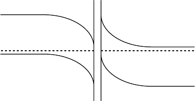
FIGURE 4.12 VBM for n-type and p-type with same Fermi energy.
of the GaAs since n-type and p-type materials can exhibit differ-
ent electrochemical potentials in contact with the same solution
(FIGURE 4.12). For a fixed position of the Fermi level, it is clear
that the potential of the valence band at the surface is different.
For example, the effect of dopant type can be seen in the etching
of n-GaAs and p-GaAs by 0.3N NH
4
OH/0.1N H
2
O
2
where room
temperature rates for n-type are about 0.19 μm/min while p-type
etches at about 0.13 μm/min.
Exposure to bright light while in a wet etchant can produce pho-
togenerated electron-hole pairs. The holes in the valence band of
n-GaAs move to the surface due to the surfacefieldandcanenhance
the etch rate (photochemical etching.) The photons effectively play
the same role as the chemical oxidant, such as H
2
O
2
. Illumination
of p-type GaAs has a minimal effect since its surface band bending
is in the opposite direction of that in n-type GaAs.
Additional doping-dependent differences can occur when a
metal is in close proximity and exposed to the etching solu-
tion. Local electrochemical effects can lead to unexpected etching
profiles with either enhanced or suppressed etching due to the
completion of a local galvanic cell; this is discussed further in
Section 4.7.
4.7 ELECTROLYTIC EFFECTS IN WET ETCHING
Electrochemical etching is often considered in terms of the driving
of a chemical reaction by the deliberate application of an applied
bias from an external voltage source. In the fabrication of GaAs
devices, this type of deliberate electrochemical etching does not
play a major role and will not be discussed here. Excellent books
dealing with this topic exist [10], and the reader is encouraged to
consult them should this topic be of interest.
However, unintentional electrochemical etching can occur when
a galvanic circuit is completed by the unintentional exposure of
142
Wet etching and photolithography of GaAs and related alloys
GeAuNi GeAuNi
PR
n
+
n
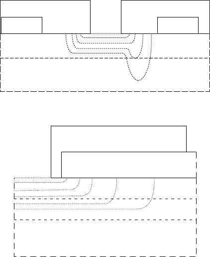
FIGURE 4.13 Effect of etching too close to exposed contact metal in FET.
n
+
n
p
+
GeAu Ni
PR
FIGURE 4.14 Rapid undercutting when approaching pn juction in HBT if
metal contact exposed to etching solution.
contact metal to the etching solution. Three examples where this
might occur are discussed here.
The first two cases may occur when a portion of the ohmic metal
is not isolated from the etching solution with photoresist. The
dotted lines in FIGURE 4.13 represent the profile of the etching
surface as the etch proceeds. When the surface profile reaches
the point where separation between the etching solution and the
metal contact is of the order of 0.25 μm, a galvanic circuit through
the solution, semiconductor and metal is completed and the etch
rate rapidly and uncontrollably accelerates. This leads to rapid
trenching into the substrate.
The second example where exposed ohmic metal can cause
accelerated etching is shown in FIGURE 4.14. As the etch front
approaches the pn junction, the lateral etch rate under the GeAuNi
metal, which is normally equal to the vertical etch rate into the sub-
strate, undergoes rapid acceleration. This leads to uncontrollable
undercutting. This problem can be avoided by using a different
metallisation, such as WSi, instead of GeAuNi.
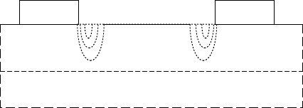
The third example is more insidious since the sample doesn’t
have to be in a solution that one would expect to be an etchant; it
occurs in DI water. A local galvanic reaction can occur where
143
Wet etching and photolithography of GaAs and related alloys
GeAuNi GeAuNi
n
+
n
FIGURE 4.15 Trenching in DI water with exposed metal contacts.
GeAuNi contacts the semiconductor, leading to trenching, as
shown in FIGURE 4.15. The depth of the trenching increases
with time, so it is very important to minimise rinse time in DI
water. Trenching can also be reduced by deoxygenating the water
by bubbling N
2
through the water (gas sparging) before rinsing.
4.8 EFFECTS OF DEFECTS AND DAMAGE
Disruption of the GaAs lattice stucture by any means will, in gen-
eral, increase the ease with which the damaged area etches. This
can be due to grown-in defects, mechanical damage, e.g. scratches,
or lattice dislocations and defects, including those generated by ion
implantation. Grown-in crystal defects tend to manifest as etch pits
with characteristic shapes. Patterned implantation can be used to
selectively enhance etching in the damaged regions. This is some-
thing to keepinmind when subsequently etching wafersemploying
implant isolation.
4.9 CONCLUSION
While wet etching has been replaced by dry etching when ver-
tical profiles are essential, there remain many cases where wet
etching remains useful. The electronic quality of the surface is
superior to that of dry-etched surfaces, and the higher degree of
compositional selectivity than generally available with dry pro-
cesses will continue to make wet etching the process of choice for
many applications.
REFERENCES
[1] H.K. Kuiken, J.J. Kelly, P.H.L. Notten [J. Electrochem. Soc. (USA) vol.133
(1986) p.1217–26]
[2] T. Takabe, T. Yamamoto, M. Fujii, K. Kobayashi [J. Electrochem. Soc.
(USA) vol.140 (1993) p.1169–80]
[3] C.I.H. Ashby [in Properties of GaAs, Eds. M.R. Brozel, G.E. Stillman
(Institution of Electrical Engineers, London, 1995) ch.18, p.707–16]
144
Wet etching and photolithography of GaAs and related alloys
[4] C.H. Hamann, A. Hamnett, W. Vielstich [Electrochemistry (Wiley-VCH,
New York, 1998)]
[5] M. Pourbaix [Atlas of Electrochemical Equilibria in Aqueous Solutions
Translator J. Franklin (National Association of Corrosion Engineers,
1975)]
[6] [Standard Guide for Development and Use of a Galvanic Series for Pre-
dicting Galvanic Corrosion Performance, ASTM Designation: G 82–83,
Annual Book of ASTM Standards]
[7] G.C. DeSalvo, W.F. Tseng, J. Comas [J. Electrochem. Soc.(USA) vol.139
(1992) p.831–5]
[8] M. Tong, K. Nummila, A. Ketterson, I. Adesida, C. Caneau, R. Bhat
[IEEE Electron Device Lett. (USA) vol.13 (1992) p.525–7]
[9] K. Kenefick [Electron. Lett. (UK) vol.21 (1985) p.558–9]
[10] J. McHardy, F. Ludwig [Electrochemistry of Semiconductors and Elec-
tronics: Processes and Device (Noyes Publications, New Jersey, 1992)]
145
Chapter 5
Dry etching of GaAs and related alloys
Chapter scope p.147
Comparison of wet and dry
etching p.147
Overview of dry etching
processes p.149
Ion-beam etching (IBE) and ion
effects in other plasma
processes p.150
Chemical dry etching p.151
Plasma etching at very low ion
energies p.152
Conventional reactive ion etching
(RIE) p.153
Halogen-based plasmas for RIE p.155
Alkane-based plasmas for RIE p.159
High-density plasma etching
(HDPE) p.160
Reactive-ion-beam etching (RIBE)
and chemically assisted ion-beam
etching (CAIBE) p.163
General issues for dry etching p.167
Etch uniformity p.167
Damage from dry etching p.168
Resists and their behaviour in dry
etching processes p.170
Advantages of Ar addition p.174
Methods for end-point
determination p.174
Plasma diagnostics for
trouble-shooting p.176
Chamber cleaning issues p.176
Effect of chamber materials p.177
Conclusion p.177
References p.178
5.1 CHAPTER SCOPE
There are five important characteristics to consider in selecting
any dry etch process. These are rate, feature profiles, compos-
itional selectivity, damage and uniformity across the wafer. In
general, the balance between chemical and physical contributions
to the etching for each type of process will largely determine
these characteristics. Chemical contributions generally produce
rapid rates, compositional selectivity and lower damage. However,
they also can decrease anisotropy (ratio of vertical to horizontal
etch rates) and can even produce either isotropic etching or etch
rates that depend on the relative reactivity of different crystallo-
graphic facets, as observed in wet etching. Physical sputtering
contributions generally increase anisotropy, but they also damage
the surface, degrading device performance that depends on near-
surface crystal quality. Consequently, the simultaneous goals of
an etch process that is both highly anisotropic and damage free are
frequently in conflict and an acceptable compromise between the
two will drive the process selection for GaAs device fabrication.
In this chapter, the many practical issues that must be considered
to successfully dry etch GaAs will be discussed.
5.2 COMPARISON OF WET AND DRY ETCHING
It is possible to etch device structures using either liquid-
phase “wet” etch processes or gas-phase “dry” processes. Both
approaches have their own advantages and disadvantages and the
best choice depends on the specifics of the application. (For advant-
ages and disadvantages of dry etching, see side note in page 149.)
Wet etch processes, in general, produce better surface elec-
tronic properties than many dry etch processes because they don’t
damage the underlying crystal lattice of the GaAs. In contrast, the
most commonly used dry processes bombard the surface with ions
having enough energy to locally disrupt the lattice, and some of
this damage may remain after the etch is completed. This problem
147
Dry etching of GaAs and related alloys
can be reduced by post-etch thermal annealing, but some damage
may remain.
Another advantage of wet etching is the ease with which it can
be used. While dry processes require gas-handling and vacuum
systems and usually complex electronic hardware to establish a
low-temperature plasma discharge, wet etching can be performed
in simple glassware on a benchtop. Chemical reagents for wet etch-
ing are also inexpensive and it is very easy to vary the chemistry.
The chemistry can be based on one of many different schemes that
oxidise the surface to yield a soluble product.
However, there are some limitations encountered with wet etch
processes. It is much harder to control the profile of a feature that
has been wet-etched. The etch undercuts the mask to a depth com-
parable to the vertical etch depth. This limits the smallest critical
dimensions that can be achieved. The profile may be diffusion
controlled (isotropic) or it may depend on the different etch rates
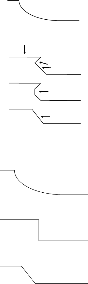
of different crystallographic faces (FIGURE 5.1). This can intro-
duce a strong dependence of the final features on how the pattern
is aligned with the GaAs wafer’s crystal planes.
Isotropic
(100)
Crystallographic
(110)
(111)
(111)
FIGURE 5.1 Isotropic profile
and crystallographic profiles of
wet etch.
undercut
vertical
overcut
FIGURE 5.2 Range of profiles
from undercut (isotropic) to
vertical to angled for RIE etching.
Wet etch rates often vary significantly with changing temperat-
ure and with how recently the solution has been mixed. This can
make run-to-run reproducibility difficult to achieve.
Dry etch processes can provide excellent profile control. The
energetic ion bombardment increases the etch rate on the exposed
surface relative to those regions protected by the mask, so ver-
tical sidewalls with negligible undercutting are readily achieved.
Depending on the balance between chemical and physical con-
tributions to the dry etch, it is possible to vary the profile from
isotropic/crystallographic to vertical to angled (FIGURE 5.2).
With vertical profiles, smaller critical dimensions are achievable.
The ion enhancement also removes the dependence on the pattern
alignment relative to the wafer crystal planes.
The primary disadvantage of dry etch processing is the degrad-
ation of electronic properties that results from both the mechanical
displacement damage and the charge-induced damage to the lattice
that are produced by ion bombardment. An additional disadvant-
age is the limited number of possible chemistries that are useful for
etching GaAs and related compounds. In general, one is restric-
ted to halogen and hydrocarbon etch chemistries since gas-phase
reactants and volatile products are required for successful dry etch-
ing. Another disadvantage of an ion-bombardment-dependent etch
is the erosion and heating of the resist by sputtering and sometimes
chemical etching. This increases the probability of ruining a device
because the resist fails before the etch process is complete.
In general, if feature profile and tight control of dimensions
are less important than surface electronic quality, a wet etch
148
Dry etching of GaAs and related alloys
may be the process of choice. If vertical or controlled-angle pro-
files and small dimensions are needed, a dry etch that achieves
the best compromise between feature profile and damage may be
preferred.
Advantages of dry etching
1) Good dimensional control
2) Excellent profile control: vertical to
controlled angle.
Disadvantages of dry etching
1) Ion-induced surface damage
2) Limited number of chemistries
3) Resist erosion can limit depth
4) Hazardous reactant gases
5) Expensive hardware
5.3 OVERVIEW OF DRY ETCHING PROCESSES
There are several types of dry etch process. Each will be discussed
separately below, but there are many features common to several
and a thorough knowledge of the important characteristics of each
will help one select the best process for a particular application.
Types of dry etching
1) Ion-beam or sputtering
2) Chemical dry etching
3) Plasma etching
4) Reactive ion etching
5) High-density plasma etching (ECR
or ICP)
6) Reactive-ion-beam etching
7) Chemically-assisted ion-beam
etching
The simplest type is ion-beam or sputter etching. No reactive
gas is used and physical sputtering of the GaAs by the incident
high-energy ions is the only mechanism involved.
In chemical dry etching, no plasma is employed or a plasma
is remotely located without line-of-sight to the sample so no ion
bombardment is involved. A component of this will be present in
every plasma process and must be considered as a possible effect
before striking the plasma or after the plasma is quenched.
Plasma etching is used here to designate the situation where the
wafer sits within the plasma but not on a powered electrode so the
incident ion energies will usually be less than 20 eV, and typically
of the order of 10–15 eV. Highly reactive radicals, formed by dis-
sociating the source gas, react faster with the surface than what one
sees in simple chemical dry etching, but ion bombardment effects
are negligible.
Reactive ion etching (RIE) has long been the standard dry pro-
cess where reactive radicals and ions are formed and the ions are
accelerated into the wafer at energies >50 eV to produce a mechan-
ism that combines both chemical etching and physical sputtering.
The same radio frequency (RF) power supply is used to generate
the plasma and accelerate the ions into the wafer.
High-density-plasma etching (HDPE) uses two separate power
supplies with one generating the plasma and the second one provid-
ing the RF power that controls the ion bombardment energy. The
source gases are more efficiently dissociated than in regular RIE
(by up to two orders of magnitude) using microwaves and magnets
to establish electron cyclotron resonance (ECR) or using induct-
ively coupled RF power to generate the plasma. The latter is called
an inductivelycoupledplasma (ICP) system. HDPE providessemi-
independent control of the plasma chemical species, both ions
and neutrals, and the energy with which the ions hit the wafer
surface.
Reactive-ion-beam etching (RIBE) and chemically assisted ion-
beam etching (CAIBE) do not use an RF supply to provide the
149
Dry etching of GaAs and related alloys
incident ion energy. Ions are accelerated from a “remote” plasma
(not in direct contact with the wafer) using ion-acceleration
techniques similar to those in simple ion-beam etching. In RIBE,
a neutral gas is predissociated to provide a beam of highly reactive
radicals, such as Cl from Cl
2
, that strike the surface in concert with
an ion beam. In CAIBE, a beam of ions, usually Ar
+
or Xe
+
,is
directed at the wafer while it is immersed in an ambient of neutral
gas, such as Cl
2
. The smallest critical dimensions are achieved
with these techniques.
In the following sections, each of these dry etch techniques will
be discussed in greater detail. For a comprehensive tabulation of
etch rates for all these processes through 1995, see “Properties of
Gallium Arsenide” [1]. A useful compilation of reviews of vari-
ous aspects of plasma processing has been recently published [2].
Since ion bombardment effects are so important in RIE, HDPE,
RIBE and CAIBE, we will begin with a discussion of ion beam
etching.
5.4 ION-BEAM ETCHING (IBE) AND ION EFFECTS IN
OTHER PLASMA PROCESSES
Ion-beam etching (IBE) is essentially a momentum-transfer sput-
tering process where the kinetic energy of the incoming ions is
transferred to the surface atoms, ejecting them from the surface.
Although non-reactive IBE is not generally used to etch GaAs
devices, the sputtering process which can be studied in isolation in
IBE is a key feature of most other dry processes and requires con-
sideration whenever the ion bombardment energies exceed 40 eV,
as they usually do in RIE, HDPE, RIBE, and CAIBE.
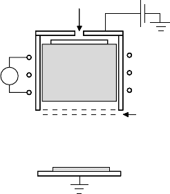
~
gas
inlet
beam voltage
13.56
MHz
ion
extraction
grids
Ar plasmaAr plasmaAr plasma
FIGURE 5.3 Ion beam etching
(sputtering).
No reactive gases are used in simple IBE. A heavy inert gas such
as Ar is typically employed (FIGURE 5.3). Lack of a chemical
component to the etch means that all materials etch at similar rates,
depending only on their relative bond strength and atomic mass.
Sputtering is more efficient when the mass of the incident ion is
closely matched to the mass of the sputtered atoms. Typical rates
for a wide varietyof materials range between0.5and 2.5 atoms/ion.
For 100 and 500 eV Ar
+
, this corresponds to a removal rate of the
order of 0.01 and 0.1 μm/min/mA/cm
2
, respectively. There is a
non-linear dependence of rate on ion energy but generally a linear
dependence on ion current density.
There is a pronounced dependence of sputtering rate on the ion
incidence angle with a maximum etch rate near an incidence angle
of 60 degrees, where surface atoms acquire a large momentum
component directed away from the surface. This leads to a charac-
teristic angled profile. When angled profiles occur in plasma-based
150
Dry etching of GaAs and related alloys
etches, it is generally an indication that a sputtering component
dominates the etch.
For a given incident ion energy, IBE is the most damaging of
processes. There is appreciable disruption of the near-surface lat-
tice by the impacting ions if they exceed the atomic displacement
energy threshold for GaAs (∼40 eV). Since this damaged region is
not partially removed by chemical reaction, more damage remains
after an IBE etch than after a plasma etch at the same ion energy.
In general, the higher the ion energy in any etch process, the more
significant the surface damage will be in degrading device per-
formance. An Ar ion energy of only 40 eV can increase a diode
ideality factor (Section 7.2.1) to 1.25 while energies of 80 and
200 eV can produce increases to 1.4–1.5 and 2.3–2.7, respect-
ively. In plasma processes where some of the damage is removed
by chemical etching, lesser device degradation will occur, but even
in these, ion energies over 100 eV generally produce some degrad-
ation and even 2 min with 60 eV ions can produce threshold voltage
shifts and transconductance decreases in FETs.
An additional effect to keep in mind is the heating of the surface
by the depositing ion energy. When it is important to avoid heating
a wafer too much, high ion energies during etching should be
avoided and, if possible, the wafer should be actively cooled during
the etch.
5.5 CHEMICAL DRY ETCHING
While device fabrication relies on plasma-based dry etching to
produce useful etch rates and the desired etch profiles for devices,
it is important to remember that GaAs can be etched by gas-
phase reactants through ordinary chemical reactions in the absence
of any plasma. Such reactions are isotropic or crystallograph-
ically rate-dependent, similar to wet etching reactions. Since
these reactions are thermally activated reactions of molecular spe-
cies rather than relatively temperature-independent reactions of
highly reactive atoms or other radicals, they tend to be quite
slow at room temperature. However, they can become signific-
ant at higher temperatures. Since wafers tend to heat up under
ion bombardment, temperatures over 100
◦
C may occur rather
routinely after long etches and simple thermal etching may be
appreciable. A rate of 0.01 μm/min has been observed at 100
◦
C
with tenths of a mTorr of Cl
2
and rates up to 0.2 μm/min are
possible at 300
◦
C. Consequently, letting a sample sit for exten-
ded periods without plasma but still exposed to Cl
2
-containing
gas mixtures may produce unintended etching whose isotropic
character could degrade device profiles. Leaving the wafer in the
151