Baca A.G., Ashby C.I.H. Fabrication of GaAs Devices
Подождите немного. Документ загружается.

Cleaning and passivation of GaAs and related alloys
of the actual III–As semiconductor in the oxide-etching solution.
Phosphide semiconductors such as InP and InGaP can etch in HCl-
based solutions without the addition of oxidiser. It is worth noting
that the main difference between cleaning and etching solutions
for III–V semiconductors is the addition of an oxidising agent to
form an etching solution that continually produces fresh oxide for
the acid or base to dissolve. Consequently, any wafer that has been
etched may have an oxide on the surface that is at least as thick
and possibly thicker than the native oxide.
Depending on the particular acid or base employed, the surface
stoichiometry of the deoxided surface may be different. A surface
may be either Ga-rich, As-rich or nearly stoichiometric (equal
amounts of Ga and As), depending on whether one element is
preferentially removed by the cleaning solution. Acidic cleaning
solutions tend to leave an As-rich surface due to their preferen-
tial reaction with Ga. Surface studies of GaAs deoxided with HCl
and H
3
PO
4
show evidence for Ga-Cl and Ga-PO
4
bonding before
the surfaces are rinsed with DI water [1]. Water rinsing effectively
removes the anions. However, neither HCl nor H
3
PO
4
react effect-
ively with As; this results in a surface enrichment of elemental As.
When these cleans are performed in a nitrogen atmosphere, the As
remains unoxidised. When performed in air, the elemental As can
oxidise upon removal from the solution. More As is seen with the
HCl solution than with H
3
PO
4
. As will be discussed in Section 3.3
on passivation, a surface excess of As can be highly undesirable
from an electronic perspective.
In contrast to its low solubility in acids, As dissolves readily in
basic solutions. Consequently, NH
4
OH solutions preserve a more
nearly stoichiometric surface (Ga/As = 0.99). The As surplus left
by acidic solutions can be removed by a step-wise treatment with
HCl, water, NH
4
OH and then water. Changing the solvent system
can affect the stoichiometric ratio. While HCl/H
2
O leaves an As-
rich surface, diluting the concentrated HCl with ethanol instead
of DI water produces a surface closer to stoichiometric (Ga/As =
0.93) [2]. A solution of (NH
4
)
2
S will dissolve oxide, but it has the
additional property of reacting with the surface to produce cova-
lently bound sulphides. As discussed extensively in Section 3.3,
this profoundly alters the electronic properties of the surface.
3.2.3 Regrowth of native oxide
Although the oxide may be effectively dissolved while in solu-
tion, a surface oxide begins to form again as soon as the surface
is re-exposed to air. For highly reproducible device results, it
is important to understand this reoxidation process and to take
72
Cleaning and passivation of GaAs and related alloys
care to handle wafers in a manner that keeps it as reproducible as
possible.
Because an oxide-free surface is hydrophobic, water beads up
on the surface as a deoxided wafer emerges from an aqueous solu-
tion. Exposure to oxygen and reoxidation of the surface begins as
soon as the water withdraws from a portion of the surface. In con-
trast to water, alcohols such as methanol and ethanol wet the deox-
ided surface. If an oxide-free surface is really important, one needs
to deoxide the surface in an oxygen-free atmosphere. This can be
easily accomplished by removing the oxide within a glove box
or a glove bag filled with nitrogen or argon. The deoxided wafer
should ideally be kept under nitrogen or argon to keep it oxide free.
Unfortunately, the transfer of the wafer into a tool for subsequent
processing, such as metallisation, will almost certainly re-expose
it to some oxygen unless a nitrogen-purged load lock is part of
the system. The base pressure of a typical electron beam metal
evaporator is a few 10
−7
torr. At this pressure, the time to adsorb
a monolayer of gas is a few seconds. It also takes tens of minutes
to pump the system down to that level. A monolayer can form in
a few milliseconds at atmospheric pressure. Since most of these
tools do not include load locks, some reoxidation is inevitable.
The reoxidation of a deoxided GaAs surface is characterised
by at least two types of reaction sites [2]. One site is extremely
reactive with even trace oxygen in a nitrogen atmosphere. Surface
studies that monitor the O 1(s) signal are more sensitive to the total
amount of oxygen present than are the more typical XPS (X-ray
photoelectron spectroscopy) studies (FIGURE 3.1) that monitor
the oxidation state of Ga and As species at the surface. Oxide
removal under nitrogen using 1 : 20 NH
4
OH/H
2
O or using 1 : 10
conc. HCl/ethanol leave surfaces with 7 and 4 atomic %, respect-
ively, as measured by the O 1(s) signal. Wafers cleaned in air
exhibit 2–3 times more residual oxide signals than those cleaned
under nitrogen gas originating as boil-off nitrogen from a liquid
nitrogen tank (the most common type of nitrogen gas available
in fabs and labs). The lower value achieved with HCl/ethanol is
probably due to a reduced time of exposure to trace oxygen in the
nitrogen gas while the ethanol wets the surface before loading in
the UHV chamber for analysis.
Additional sites on the surface reoxidise more slowly over a
period of minutes, as measured by changes in the photolumines-
cence intensity. Photoluminescence as a method for monitoring
surface composition is discussed in Section 3.3.2. The most uni-
form device results may be expected when care is taken to perform
subsequent process steps with the times between and the times for
those subsequent steps being as uniform as possible following
deoxidation. The presence of oxygen at the interface between a
73
Cleaning and passivation of GaAs and related alloys
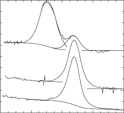
1334 1329 1325 1321 1316
binding energy, eV
N(E)/E
As(2p
3/2
)
native oxide
HCl/EtOH
NH
4
OH
FIGURE 3.1 As(2p
3/2
) XPS spectra showing chemical shift for As bound
to O in native oxide versus “oxide-free” surfaces.
contact metal and GaAs can affect the process metallurgy and the
formation of defects at the interface, so consistency in cleaning
can be important in determining consistency in contact behaviour.
The structure of the surface oxide can depend on how it was
formed. When an oxide is grown by thermal oxidation at 420
◦
Cto
a thickness of about 4 nm, the oxide is Ga-rich with an As gradi-
ent that has more As-oxide present as one moves towards the free
surface. In contrast, an ECR-plasma-grown oxide of comparable
thickness is nearly stoichiometric (equal amounts of Ga and As)
and contains a larger amount of As
+5
versus As
+3
than does the
thermal oxide [3]. These differences may be due to the products of
the thermal oxidation being determined by their relative thermo-
dynamic stability while the plasma oxidation is controlled more by
the kinetics of the reactions. XPS results suggest that the thermal
oxide is somewhat closer to Ga
2
O
3
while the ECR plasma oxide is
closer to the stoichiometric GaAsO
4
. In either case, the quality of
the semiconductor-oxide surface is equally poor in terms of inter-
face charges in C-V measurements after deposition of PECVD
SiO
2
and Al metallisation. Composition, structure and electronic
surface quality are the topics of Section 3.3.
3.3 PASSIVATION OF GaAs
The term “passivation” carries with it some rather distinct yet
related connotations. The first deals with the alteration of the
74
Cleaning and passivation of GaAs and related alloys
surface of the semiconductor to achieve more favourable electronic
properties than those obtained with the native oxide. The second
has to do with protection from reaction with the ambient over the
lifetime of the device. Since reaction with the ambient, especially
oxygen, can alter the electronic properties, even a device with
excellent initial operating characteristics may gradually degrade
over time. The third common use of the term “passivation” relates
to the deactivation of dopants or defects through reaction with
readily diffusing species such as H atoms. Surface treatments
and especially plasma processing conditions can be a source of
hydrogen that can diffuse deeply into the semiconductor before
reacting with a dopant or a defect. While defect passivation is
generally desirable, dopant passivation alters free carrier concen-
trations and can negatively affect device performance. This third
type of “passivation” will be discussed in Section 5.7.2.
We will begin this section with a discussion of the physical and
chemical issues that affect the important surface and interfacial
electronic properties of GaAs. Since reaction with the ambient,
especially oxygen, can alter critical electronic properties, we will
conclude with a discussion of some methods that seek to isolate
the surface from such effects.
3.3.1 Electronic properties of the GaAs surface
The bulk electronic properties of semiconductors in general and
GaAs in particular were discussed in Section 2.2. Many of the con-
cepts, such as band structure and bandgap, are derived assuming
the three-dimensional translational symmetry of an infinite bulk
crystal. However, the presence of a surface immediately introduces
different boundary conditions that make the bulk description no
longer adequate. The most significant effect of the surface is the
introduction of additional energy levels that may lie within the
forbidden energy gap between the valence and conduction bands.
The number and energy of these levels, called surface states, will
determine how important they are in controlling the electronic
behaviour near the surface.
An abrupt termination of the three-dimensional crystal lattice
would leave surface atoms coordinatively unsaturated with many
unpaired electrons; this would produce an unacceptably high-
energy state. In reality, this condition is avoided by either surface
reconstruction or reaction with other chemical species that may be
present.
In surface reconstruction, the surface atoms move from their
hypothetical bulk positions into positions where they can bond
with each other to reduce the total energy. There are a vari-
ety of different reconstructions that can occur, depending on the
75
Cleaning and passivation of GaAs and related alloys
particular exposed crystal face and whether the surface is primar-
ily terminated by Ga or As atoms. Since the GaAs(100) surface
is of the greatest technological importance, we will restrict most
of our discussion to that crystal face. However, any mesa-type
device will have other crystal faces exposed on the sidewalls. The
ideal GaAs(110) surface, which is a natural cleavage facet and
can be obtained as vertical facets by crystallograpically selective
etching (Section 4.3.2), is supposed to be free of surface states
within the bandgap; however, real device facets can be expected
to deviate somewhat from ideal since they are not perfectly planar.
The kinks and steps found on surfaces that are not planar at the
atomic level can introduce additional energy states. Many studies
of the surface structure of GaAs(100) using LEED (low-energy
electron diffraction) or RHEED (reflection high-energy electron
diffraction) have been reported. From the LEED electron diffrac-
tion patterns, it is possible to determine the crystal symmetry of
the surface layers; from the LEED geometry, the possible atomic
arrangements are deduced. There are a number of reported recon-
structions for GaAs(100) depending on the history of the surface,
and they have different work functions, i.e. energies relative to
the vacuum level. This is to be expected since they will have dif-
ferent surface electronic states that determine the work function.
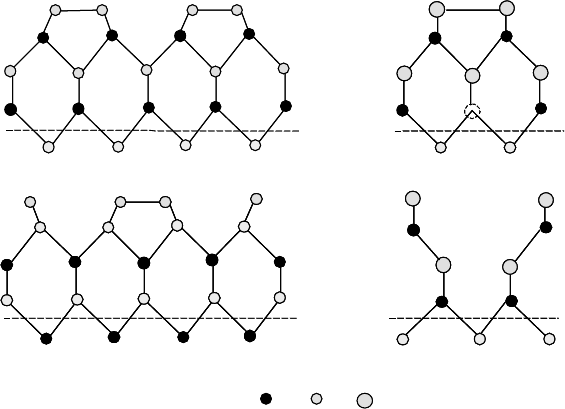
Some surface geometries are shown in FIGURE 3.2. While it is
possible to measure structures of carefully prepared samples under
ultra-high-vacuum (UHV) conditions (<10
−8
torr), it is important
C(2×1)
with S
(100)
C(2×1)
with S
(100)
GaAs S
(2×4)
(100)
C(4×4)
As rich
(100)
FIGURE 3.2 Side view of C(4×4) and (2×4)GaAs(100) and C(2×1)S of
sulphided surface.
76
Cleaning and passivation of GaAs and related alloys
to remember that the surface of an actual device will not usually
have a perfectly planar topography, exposing only one crystal
plane, nor will it be in UHV. Therefore, great care must be taken
in concluding which scientific studies will map appropriately onto
the situation for a particular device.
The thermal history of the wafer can profoundly influence its
surface structure. It is common to describe a surface geometry
using (A×B) nomenclature. For example, the (2×4) surface recon-
struction refers to a two-dimensional unit cell that is 2× larger in
one direction and 4× larger in the other direction compared to
the bulk unit cell. If a GaAs wafer capped with amorphous As
in an MBE machine to prevent oxidation is heated in vacuum to
380
◦
C, it assumes a C(4×4) geometric structure with 1 mono-
layer of adsorbed As. If it is further heated to 480
◦
C, it assumes
a(2×4) geometry. Further heating to 600
◦
C without an As over-
pressure converts it to (4×1) with a slight excess of Ga on the
surface [4]. Reactions with species such as oxygen or sulphur pro-
duce other changes in the surface geometry. While it is possible
to obtain well-defined geometries under controlled vacuum con-
ditions, great care must be taken in extrapolating the results to
real-world wafers undergoing device fabrication. The character of
the surface may be very different from that described in the literat-
ure, and very different behaviour may result when that is the case.
Nevertheless, such studies can provide starting points for thinking
about the condition of a particular wafer.
An alternative way to lower the surface energy is by reaction
with the ambient, especially with oxygen, to form an oxide sur-
face. This will generally be the condition of the GaAs surface
unless deliberate effort has been taken to remove the oxide and
replace it using a more favourable surface reaction. A major goal
for many years has been the achievement of an insulator/III–V
interface of the same quality as the nearly ideal SiO
2
/Si inter-
face that is the foundation of CMOS technology. Unfortunately,
unlike the SiO
2
/Si interface with its extremely low density of
interface states (as low as 10
9
/cm
2
) and a very high-quality
oxide yielding trapped charge densities of about 10
10
/cm
2
, the
oxides of III–V semiconductors suffer from many interface states
that are located within the bandgap. This is true whether the oxide is
formed thermally or by plasma oxidation. For GaAs with its native
oxide, the density of these interface states is in excess of 10
13
/cm
2
,
roughly one state for every 100 surface atoms. This high interface-
state density results in Fermi level “pinning”, as discussed
below, and has so far precluded a successful metal-insulator-
semiconductor (MIS) technology in the III–V systems. The
majority of “passivations” involve reactions whose products are
meant to be more electronically favourable than the native oxide.
77
Cleaning and passivation of GaAs and related alloys
Replacement of the native oxide with an alternative interfacial
species is essential because the formation of the native oxide itself
can generate defects that ensure poor electronic behaviour [5].
During the initial period of oxidation with atomic oxygen, even
before a general disruption of the GaAs lattice or the formation
of unstable arsenic oxides that can liberate elemental As (Sec-
tion 10.2.1), oxygen atoms displace the top-layer As atoms and
bind to the second-layer Ga atoms. Scanning tunnelling micro-
scopy (STM) of GaAs (100) with the (2×4) surface structure has
shown that the displaced As atoms localise in surface trenches and
on top of surface As-dimer rows to place As atoms in what would
normally be Ga sites, forming the donor As
Ga
antisite defect and
an acceptor state that may be associated with an undimerised As
atom with a half-filled dangling bond. Increases in total O cover-
age lead to preferential formation of oxygen dimers on the surface
with reduction of the undimerised As sites. Such dimer formation
appears to be the natural step for oxidation with molecular oxygen.
In addition, metallic clusters of As atoms can form as the oxygen
reaction proceeds. With sufficient oxidation, the Fermi level is
pinned for p-GaAs somewhere between 0.75 and 0.5 eV, which
are the energy levels for singly and doubly ionised As
Ga
antisite
defects.
Vapour deposition of Ga
2
O
3
oxide onto GaAs in vacuum can
minimise the formation of As-oxides. This is significant because
As
2
O
3
is thermodynamically unstable in contact with GaAs, with
the reaction
As
2
O
3
+ 2GaAs → Ga
2
O
3
+ 4As
being thermodynamically favoured (ΔG
0
=−62 kcal/mol).
Vapour-deposited Ga-oxides [6] have shown some of the best elec-
tronic behaviour to date (FIGURE 3.9), but problems still remain
(Section 3.3.5).
An important point to remember when considering surface reac-
tions is that even a partial monolayer of reactedmaterialcan domin-
ate the electronic structure of the surface or interface. The chemical
bonding of the surface monolayer defines the energetics of the
interface states and determines whether they lie within the bandgap
(undesirable) or not (highly desirable). Therefore, the preparation
and cleaning of the surface before any passivation process may
totally dominate the results and great care must be taken to ensure
reliable and reproducible results. When differences between liter-
ature predictions and personal fabrication results occur, they can
often be traced to differences in the starting surface condition.
A word of caution is in order about relying simply on surface
stoichiometry or geometry as a predictor of electronic properties.
78
Cleaning and passivation of GaAs and related alloys
The surface state energies and the density of states at each energy
are not merely dependent on what chemical elements are at the
surface. Details of the bonding configuration of those atoms will
determine the energetics of the surface, and the same nominal com-
position can display quite different bonding. The standard methods
of identifying surface chemical composition, like Auger electron
spectroscopy (AES), X-ray photoelectron spectroscopy (XPS),
secondary ion mass spectrometry (SIMS) or energy-dispersive
X-ray analysis (EDS, EDX or EDAX) typically are not sensit-
ive to species that are present below a tenth of a percent. However,
elements present at even lower levels can be not only important but
even dominant in determining surface electronic properties if they
are properly positioned within the forbidden gap and exhibit rapid
recombination kinetics. Additionally, it is possible for surfaces
of different elemental compositions to assume the same geometric
pattern as measured by LEED, so having the same structure should
not be construed as convincing evidence of the same chemical
composition and same electronic properties.
Either reconstruction or chemical reaction will introduce surface
states that generally serve as traps for free carriers. These levels
may be quite discrete or they may be spread over a band. Both
electron and hole surface traps are known. Elements that are more
electronegative than Ga and As, such as oxygen, act as electron
acceptors. The more electronically deleterious states tend to lie
toward the middle of the gap and are called “midgap states”.
3.3.1.1 Midgap states and Fermi level pinning
The Fermi level and its position relative to the valence band max-
imum, VBM or E
V
, and conduction band minimum, CBM or
E
C
, are discussed for bulk semiconductors in Section 2.2.2. The
presence of midgap states at the surface or interface can have a
profound effect on the Fermi level position relative to the VBM
and CBM near the surface, as illustrated in FIGURE 3.3 for an
n-type semiconductor.
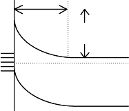
N
s
E
f
E
C
E
V
d
f
S
FIGURE 3.3 Fermi level pinning
at energy of midgap surface states.
When there are surface states lying below the Fermi level, they
will be filled by electrons from the conduction band. When there
are N
s
states per cm
2
below the Fermi level, the surface will acquire
a negative charge equal to −eN
s
/cm
2
. This will repel electrons
from the surface region and produce a depletion region nearly
devoid of free electrons which will have a positive space-charge
approximately equal to +eN
d
d, where N
d
is the donor atom con-
centration and d is the depth of the space-charge region. There
is a strong electric field directed towards the surface that opposes
the flow of more electrons into the unoccupied surface states. The
Fermi level in the bulk is aligned with the top of the filled surface
79
Cleaning and passivation of GaAs and related alloys
states, and the energy of the surface is raised relative to the bulk
by the surface potential, φ
s
. An exact determination of φ
s
requires
the solution of Poisson’s equation with appropriate boundary con-
ditions. For simplicity, one may assume that the space charge ρ is
equal to eN
d
d from the surface to a depth, d, where d = N
s
/N
d
.
The surface potential, φ
s
, is then given by eN
2
s
/2N
d
, where is
the semiconductor permittivity. The energy by which the bands
are raised at the surface is approximately ΔE = eφ
s
. If the surface
potential is sufficiently high that the valence band at the surface
becomes closer to the Fermi level than the conduction band is,
the near-surface region becomes effectively p-type and an inver-
sion layer is formed. The response of these various quantities to
externally applied voltages is discussed in Section 7.2.1.
When there is an extremely high density of midgap surface
states, as in the case of GaAs(100), the Fermi level is effectively
pinned at the energy corresponding to that of the midgap states.
Changing applied voltages may merely move carriers into and out
of surface states, leaving the position of the Fermi level unchanged
and “pinned” at the surface-state energy. The primary goal of sur-
face passivation is the unpinning of the Fermi level. Changing the
chemical composition of the surface layer will change the energy
of the dominant surface states. If the new surface states are moved
close to the VBM or CBM or, even better, are moved out of the
forbidden gap, the Fermi level can become unpinned. However,
changing the surface composition may serve merely to pin the
Fermi level at another position within the gap if there is still a high
density of midgap states at the new energy position.
Fermi level pinning can occur at a wide range of inter-
faces. It is seen at “clean” semiconductor surfaces grown by
MBE, naturally oxidised surfaces, chemically modified sur-
faces, semiconductor/insulator interfaces, metal/semiconductor
interfaces and regrown semiconductor/semiconductor interfaces.
While the remainder of this chapter will be focusing on chem-
ical modification of exposed surfaces, most work on Fermi
level pinning has been directed towards the understanding of the
metal/semiconductor interface because of its importance in device
performance.
A number of models have been put forth to explain the ori-
gin of Fermi level pinning and its effect on the Schottky barrier
height [7] of Schottky contacts (Chapter 7). These include the
unified defect (UDF) or advanced unified defect (AUD) models
of Spicer et al., the metal-induced-gap state (MIGS) model of
Heine and later Tersoff, the disorder-induced gap state (DIGS)
model of Hasegawa and Ohno, and the effective work function
(EWF) model of Woodall and Freeouf. The proposed origin of
the pinning states varies with the model employed. In the UDF
80
Cleaning and passivation of GaAs and related alloys
model, pinning is ascribed to deep levels related to stoichiometric
variation, especially the As antisite. In the MIGS model, the
midgap states originate in the penetration of the metal wave func-
tion into the semiconductor. In the DIGS model, the pinning states
result from the loss of two-dimensional periodicity due to disorder
of the bonding at the interface. In the EWF model, pinning occurs
at metallic clusters formed by precipitation of As at the interface.
The most appropriate model for a particular case varies with the
details of the interface.
It is important to remember that band bending is caused by the
total surface charge. This charge is the combination of surface-
trapped charge due to surface states lying within the forbidden
gap and surface-fixed charge, i.e. ionic charge on the surface that
may not be related to the surface traps. With only a surface-fixed
charge, the Fermi level can still move freely. In contrast, with
sufficiently high densities of surface-trap states, the Fermi level
is pinned and neither bulk doping nor externally applied electric
fields can move it.
Band bending due to surface-fixed charge can repel minority
carriers sufficiently to reduce the surface recombination velocity
(Section 3.3.1.2). The change in the surface recombination velo-
city as a function of forward injection parameters can provide a
measurement of surface-fixed charge and help distinguish contri-
butions from fixed charge and surface states. Better results will be
obtained if injection of carriers by absorption of light is avoided.
3.3.1.2 Recombination and surface recombination
The free carriers in a semiconductor participate in a dynamic pro-
cess with the constant generation and recombination of individual
carriers determining their concentration in a particular region of
the material. The details of these processes are outside the scope
of this book and are discussed quantitatively in many books on
semiconductor and device physics [8]. The free carrier concen-
tration in a particular region of the wafer or device is determined
by the balance between generation and recombination. Dopant
atom concentrations, temperature and illumination are the factors
that dominate the generation process. The equilibrium concentra-
tions of electrons and holes are discussed in Section 2.2.2 for the
situation without illumination. Illumination will alter these con-
centrations by producing an equal number of electrons and holes
when and where photons are being absorbed in the material. The
location of creation depends on the absorption coefficient of the
semiconductor; there is an exponential decrease in the number
of photogenerated carriers as the light penetrates deeper into the
material. The carriers generated within a region of depth dx is
81