Baca A.G., Ashby C.I.H. Fabrication of GaAs Devices
Подождите немного. Документ загружается.

Cleaning and passivation of GaAs and related alloys
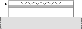
QW
InGaAs
InGaAs
InP cap
FIGURE 3.14 Regrowth for buried distributed feedback Bragg (DFB) grating.
While a new wafer fresh from its sealed container has minimal
contamination, a wafer that has been etched to produce a non-
planar surface morphology may have significant contamination
levels prior to the final cleaning before insertion into the growth
chamber for regrowth.
For example, in making edge-emitting distributed feedback
(DFB) lasers, one may want to etch a Bragg grating into the surface
of a wafer, placing it relatively near to the active waveguide core
where the mode intensity is highest. Following etching of the grat-
ing, the wafer must be cleaned, reinserted into the growth chamber
and have a cladding layer grown over the grating. A schematic of
such a device is illustrated in FIGURE 3.14.
Obviously, the native oxide needs to be largely removed with
either an acidic or a basic solution. Similarly, metal-ion contamina-
tion can be reduced by rinsing with NH
4
OH. This has already been
discussed in Section 3.2. However, unless these treatments and
the loading into the growth chamber are conducted with the com-
plete exclusion of oxygen, some surface oxide will have reformed
by the time the wafer loading is completed. This reoxidation can
be minimised by sulphiding the surface of the wafer to block the
reactive sites where oxygen would bond; it is, nevertheless, still
important to minimise oxygen exposure. Higher quality interfaces
have been reported using sulphur to retard oxidation while prepar-
ing a sample for regrowth. While the sulphur does not completely
prevent reoxidation, it does retard it and makes it easier to obtain
a clean surface for regrowth.
3.3.4 Passivation for improved contact metallisation
A crucial part of fabricating good devices is making good con-
tacts; Chapters 6 and 7 are devoted to this important topic. This
section will discuss some of the materials issues related to met-
allisation and how the presence of a passivating layer may alter
the interactions of metals with GaAs. The issues that are import-
ant in metallisation of unpassivated surfaces are largely the same
for metallisation of passivated surfaces. The deposited metal may
undergo reaction with the GaAs surface to form new chemical
phases. By changing the chemical nature of the interface, the
102
Cleaning and passivation of GaAs and related alloys
passivant may profoundly alter alloy formation, defect genera-
tion and atomic interdiffusion. There can be the removal of some
surface/interface states and the introduction of new ones. The chal-
cogens, S and Se, are n-type dopants, so there may be a change in
the near-surface doping level of the semiconductor. This may be
highly desirable for making better contacts but it should be borne
in mind when considering the sources and sinks of free carriers
in a device design. Thermal annealing following metallisation can
cause chemical reaction and defect or dopant diffusion. Exten-
ded operation under bias can induce changes. The deposition of
an encapsulant can passivate dopants or defects by injection of H
or, if a plasma process, it can introduce surface damage. In addi-
tion, the encapsulating process may cause loss of the passivant or
change near-surface doping by generating donors from the pas-
sivant. We shall address how passivation affects several of these
issues in the following section. While the standard approach at the
time of writing this chapter is to metallise unpassivated surfaces,
that may change with further understanding and development of
suitable passivation procedures.
When a metal atom is deposited on the surface of GaAs, it often
undergoes reaction with the GaAs, leading to disruption of the
interface and formation of a mixed composition in the near-surface
region. Sometimes extensive interdiffusion and alloying between
the metal and the semiconductor occurs, changing the elemental
composition of both to an appreciable distance from the nominal
interface. This generally requires some heating for these reactions
to proceed over more than a few atomic layers. The formation of
such interfacial compounds may be an important part of forming a
good contact, as will be discussed in Chapter 6 concerning ohmic
contacts, but it can also be a problem, especially if it occurs in a
non-uniform fashion. The common mechanisms involved in the
formation of ohmic contacts are outlined in Section 6.2.3 with the
example of Ge/Au/Ni, one of the most popular ohmic formulations
for n-GaAs. The initial step is reaction of Ni with the native oxide
to allow more uniform access of the other elements to the actual
GaAs surface. It is obvious that prior replacement of oxygen with
sulphur or another passivant can have a major impact here. Sub-
sequent steps, such as reaction with Ni to disrupt the lattice with
Ni-GaAs complexes, could also be modified by formation of metal
sulphide interlayers. Since diffusion in semiconductors is defect-
mediated, changes in defect locations and populations through
passivants acting as diffusion barriers may play an important role.
Diffusion of As to the contact surface can leave voids that are
filled by stable intermetallics, such as AuGa and NiGe. Localised
excessive reaction can produce “spiking”, the deep penetration of
the conductive intermetallic in a small region, shorting the device.
103
Cleaning and passivation of GaAs and related alloys
To the extent to which passivation may affect any of these steps,
it may be desirable or undesirable in forming ohmic contacts.
The potential importance of passivation in the formation of
Schottky contacts is immediately obvious. The Schottky barrier
is key to their operating characteristics (Section 7.2), and that is
defined as the energy difference between the metal Fermi level and
the semiconductor conduction band energy (for n-type) or valence
band energy (for p-type) at the metal/semiconductor interface.
Clearly, any effect a passivant may have on Fermi-level pinning
through the energy and number of surface states may affect the
behaviour of a Schottky contact.
A key reaction occurring in many good ohmic contacts is form-
ation of the AuGa alloy at the interface. The formation of this alloy
is affected by the presence of oxide on the surface, with alloy form-
ation enhanced by oxide relative to that on a bare GaAs surface
(deoxided in UHV before Au deposition) and As atoms segreg-
ating on the metal overlayer during Au deposition. When a thin
film of Au is deposited on GaAs with its native oxide (even after
nominal oxide removal with a wet etch), Au reacts with GaAs to
form an AuGa alloy and releases elemental As, which segregates
on the surface of the Au metal [19]. A similar reaction between
the native oxide and Ni has been identified. Sulphiding the surface
with (NH
4
)
2
S
x
delays both the formation of the AuGa alloy and
As segregation for very thin Au layers (5 Å), but the alloy and As
form as the deposition proceeds. Since the “sulphided” surface still
had some oxygen bound, these results are somewhat inconclusive
as to what would happen with a fully sulphided surface.
Silver, in contrast, does not react with GaAs at room temperat-
ure and a comparable AgGa alloy is not obtained with either the
oxided or sulphided surface. With the less reactive Ag, there is still
evidence for formation of Ag-S bonding at the interface with the S
primarily being taken from As-S bonds [19]. For starting surfaces
without excess As, as in the UHV annealed case, the Ag-S forms,
but it is by displacement of Ga from Ga
x
S
y
and a small amount of
Ga metal appears due to displacement by formation of Ag sulphide.
With further Ag deposition, the Ag deposits as Ag metal clusters
and does not react chemically with GaAs. While these differences
may seem slight, the interface states depend intimately on the
details of bonding at the interface and such seemingly subtle dif-
ferences might actually have major consequences for the number
density and energies of interface states. They can also have very
different effects on the number of vacancies and other defects that
can be electronically active or affect diffusion in the material.
Indium does not normally react with the GaAs-oxide so its initial
deposition on a native-oxide surface proceeds by island growth.
With a partially sulphided surface, layer-by-layer growth through
104
Cleaning and passivation of GaAs and related alloys
the apparent formation of a thin InGaAs alloy was observed. On
the sulphided surface, the In caused a shift in the Fermi-level pos-
ition towards the Schottky limit. In contrast, for Au the position
of the Fermi level did not appear to depend on whether the surface
had the native oxide or was partially sulphided. Starting with an
oxide-free, Ga-rich surface that has been sulphided [20], there was
an initial formation of an In
x
S
y
interfacial layer where In appears
to react with surface sulphur dimers. However, no further inter-
mixing between In and GaAs is observed and further In addition
is metallic. The In/S/GaAs structure has a higher Fermi level than
In/GaAs. This change in barrier height may be in part due to a
sulphur-induced interface dipole.
The results of these two sets of parallel studies illustrate how
vitally important it is to be careful before assuming the results of
anylaboratory study may pertain directly to real device fabrication.
The often “ideal” starting conditions for the lab study may be
a poor model for the real device. The composition of the real
device surface may be quite different in terms of Ga-to-As ratios,
presence of some degree of native oxide, surface reconstruction,
etc. Consequently, promising scientific results may not translate
into better devices, and procedures that are not expected to work
based on very careful lab studies may work quite nicely.
The specific surface treatment of an Au/GaAs Schottky diode
prior to Au deposition and its thermal annealing history can
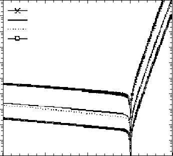
strongly influence its operating characteristics. FIGURE 3.15
shows the Schottky barrier height and dark current for Au/GaAs
and Au/S/GaAs with and without hydrogen plasma treatment [1].
Exposure to the plasma, presumably to remove oxide, without
the thin Au protective layer damages the surface and produces
poor performance relative to either acid-cleaned or S-passivated
surfaces. For the Au/S/GaAs where the Au layer was only 5 nm
thick, the atomic hydrogen can penetrate the thin metal film and
reduce As-O and As to a volatile product that escapes from the
interface. A much lower dark current results with the reduced
quantity of As at the interface. Similar improvements occurred for
Au/GaAs with atomic hydrogen. It is important to note that this
H-exposure was performed with very thin Au films, and exposure
to H with thicker Au films might not be beneficial since the As-H
products would be trapped by the thicker film even though H, with
its ready propensity to diffuse in virtually any material, could still
be reaching the interface.
With Pd metallisation, the catalytic ability of Pd to generate
atomic H from H
2
can remove the need for a plasma. The effect on
dark current of thermal anneals at different temperatures is shown
in FIGURE 3.16 [1]. While both acid-cleaned and S-passivated
surfaces displayed improved performance with H-anneals versus
105
Cleaning and passivation of GaAs and related alloys
–1.5 –1.0 –0.5 0.00.5
applied bias (V)
10
–9
10
–1
10
–8
10
–7
10
–6
1 × 10
–5
1 × 10
–4
10
–3
10
–2
hydrogenated (SBH=0.72, n =1.04)
HCl-cleaned (SBH=0.78, n =1.05)
S-passivated (SBH=0.80, n =1.03)
S-passivated/Au(5 nm)/hydrogenated
(SBH=0.85, n =1.03)
current density (A/cm
2
)
FIGURE 3.15 I-V characteristics of Au/GaAs Schottky diodes with various
surface treatments. (Kang and Park [1].)
vacuum anneals, the sulphided surface retained its low dark current
at appreciably higher temperatures than the acid-cleaned surface
and, in general, performed better. It is, as always, important to
remember that any process generating atomic H near GaAs can
lead to H-atom diffusioninto the semiconductor with resultant pas-
sivation of dopants and defects. This effect is increased at higher
temperatures and longer exposure times, so any potentially bene-
ficial effect of H must be weighed against possible deleterious
changes it may produce.
Interest in actually preventing ill-defined interdiffusion and
reaction between the metal and the semiconductor has been elev-
ated by the possibility of integrating semiconductors and magnetic
thin films to harness magnetic properties such as giant magnetores-
istance (GMR). GMR permits the controlling of the electrical
resistance by the application of a magnetic field and requires the
precise growth of a metal superlattice. Magnetic metals such as Co
and Fe are used, but these tend to intermix with GaAs. For these
metals also, a monolayer of S inhibits interdiffusion of As and Ga
and yields ferromagnetic behaviour at low metal coverages.
3.3.5 Special oxide passivations
The ideal solution for a semiconductor/insulator interface would
be a good oxide, as with Si and SiO
2
. Other approaches,
as discussed above, suffer from unacceptably high interface-
state densities. These occur for a variety of reasons including
non-stoichiometric surfaces, structural defects, thermodynamic
instability and intrinsic Fermi-level pinning due to the energy
levels for interfacial bonding.
106
Cleaning and passivation of GaAs and related alloys
vacuum (HCl-treated)
H (HCl-treated)
vacuum (S-passivated)
H (S-passivated)
vacuum (HCl-treated)
H (HCl-treated)
vacuum (S-passivated)
H (S-passivated)
1.0
0.9
0.8
0.7
0.6
0 100 200 300 400 500
anneal temperature (˚C)
0 100 200 300 400 500
anneal temperature (˚C)
Schottky barrier height (eV)
10
–6
10
–7
10
–8
10
–9
reverse leakage current (A/cm
2
)
(a)
(b)
FIGURE 3.16 Schottky barriers and dark currents for Pd/GaAs Schottky
diodes with various surface treatments following thermal annealing. (Kang
and Park [1].)
Promising behaviour has been observed with a special oxide
deposited by e-beam evaporation of single-crystal Gd
3
Ga
5
O
12
(a garnet) on As-stabilised (2×4) GaAs that had been transferred
from a solid-source MBE III–V growth chamber to the e-beam
deposition chamber at 1 × 10
−10
torr [6]. Primarily Ga
2
O
3
films
were deposited on the clean, atomically ordered GaAs(100). These
films have a non-uniform composition, with the interface being
essentially Gd-free and the Gd concentration peaking at the oxide
surface. This non-uniformity has consequences for the electronic
properties, as discussed below.
MIS capacitors were fabricated on n-GaAs with 462 Å Ga
2
O
3
and p-GaAs with 594 Å Ga
2
O
3
. Film resistivity was in excess of
10
15
-cm; quasistatic C-V measurements require greater than
10
15
-cm resistivity because they are very sensitive to cur-
rent leakage. High-frequency (up to 1 MHz) and quasistatic C-V
behaviour was measured (FIGURES 3.9 and 3.17).
107
Cleaning and passivation of GaAs and related alloys
100 Hz
1 kHz
10 kHz
1MHz
100 kHz
700
Ga
2
O
3
/p-type (100) GaAs
600
500
400
300
capacitance (pF)
200
100
0
–8 –6 –4 –20
volta
g
e (V)
2 468
quasi-
static
100 Hz
1 kHz
N
A
= 4.4 × 10
16
cm
–3
area =2.1 × 10
–3
cm
2
sweep rate = 120 mV/s
FIGURE 3.17 C-V curve for p-GaAs with e-beam-evaporated Ga
2
O
3
.
(From Passlack et al [6].)
Inversion, depletion and accumulation are all observed in the
C-V curves. Capacitance overshoot at the onset of inversion is seen
for n- and p-type and may be due to filling of trapping centres in the
oxide. There is a Fermi-level-independent time constant for trap-
ping that is longer than 1 ms, which is three orders of magnitude
greater than the theoretically calculated interface trap time con-
stant. There is also a long-term drift of the capacitance with a time
constant greater than 10 s. This is ascribed to oxide traps located
20 Å or so away from the interface. An approximately 350 mV
hysteresis is seen in the C-V curves, indicating the presence of
mobile charges.
There is frequencydispersionin accumulation that may be due to
an oxide at the interface that is relatively low resistivity rather than
due to a high density of interface states near the conduction band
edge. Conductance-voltage measurements reveal such a region in
these devices. When the insulator is inhomogeneous, containing
regions of higher electrical conductivity, the observed capacitance
will increase with decreasing measurement frequency (Maxwell-
Wagner effect).
The non-ideal electrical behaviour of these interfaces is prob-
ably due to the non-uniform composition of the oxide as one moves
away from the GaAs surface. A Terman analysis shows D
it
in the
mid 10
10
cm
−2
eV
−1
midgap and trap density in the mid 10
11
/cm
2
108
Cleaning and passivation of GaAs and related alloys
10
14
10
13
10
12
10
11
interface state density (cm
–2
eV
–1
)
10
10
E
v
E
i
energy (eV)
p-typen-type
Ga
2
O
3
/(100) GaAs
E
c
FIGURE 3.18 Density of interface states from Terman analysis C-V in
FIGURES 3.9 and 3.17. (From Passlack et al. [6].)
integrated over the gap (FIGURE 3.18). While this approach pro-
duces one of the best interfaces to date, electronic problems with
the oxide and the role of Gd in the oxide need to be resolved before
it becomes the basis for a robust MIS technology for GaAs.
3.3.6 Dielectric passivations: PECVD and ECR SiN
x
and SiO
x
N
y
In this section, we will focus on the application of dielectrics as
passivationswithoutthedeliberateadditionofa chemically distinct
monolayer passivant, such as S. Some improvements in electrical
performance can be obtained with a dielectric alone and the encap-
sulation it provides helps to stabilise the electrical characteristics
for long-term operation. An example of the improvement of an
AlGaAs/GaAs HBT is shown in FIGURE 3.7.
While both silicon nitride and SiO
2
have been employed as
dielectrics on GaAs devices, SiN
x
has been largely the dielectric
of choice due to its higher dielectric constant and its better perform-
ance as a diffusion barrier, which makes it a better environmental
encapsulant. Consequently, we will focus mainly on nominally
silicon nitride materials in this section.
Growth of a dielectric/GaAs structure with a highly controlled
and nearly ideal interface has shown what might be inherently
possible, if exceedingly difficult at present, to achieve under
109
Cleaning and passivation of GaAs and related alloys
SiN
x
/As-rich GaAs
10
14
10
13
N
ss
(cm
–2
eV
–1
)
10
12
10
11
10
10
E
v
–1.2 –1.0 –0.8 –0.6 –0.4 –0.2
E
c
SiO
2
/SiN
x
/
Ga-rich GaAs
SiO
2
/ SiN
x
/
Si ICL/Ga-rich GaAs
E – E
c
(eV)
(P4 × 6) (G4 × 6)
FIGURE 3.19 Surface state densities from different GaAs reconstructions
at dielectric/GaAs interfaces. (From Anantathanasarn and Hasegawa [21].)
normal fabrication conditions. Using a Ga-rich (4×6) reconstruc-
tion on (100) GaAs, complete unpinning of the Fermi level over
the entire bandgap with a minimum interface-state density of
4 × 10
10
/cm
2
/eV has been reported [21]. In FIGURE 3.19, the
results of Terman analyses of these high-quality interfaces are con-
trasted with nominally SiN
x
-on-GaAs surfaces, which show the
expected U-shaped behaviour of a poor interface. An Si interface-
control layer was deposited on the clean, reconstructed surface,
partially converted to SiN
x
by direct nitridation, and then coated
with a thick SiO
2
layer using plasma-enhanced chemical vapour
deposition (PECVD). Some hysteresis and flat-band voltage shifts
are observed in the C-V curves, so an ideal GaAs/dielectric
combination was not totally achieved. The effectiveness of this
approach has only been demonstrated on ideal (100) surfaces and
may not work as well on other crystal faces, such as are exposed in
mesa structures. However, it does demonstrate that a MOS-quality
interface in a real device is at least theoretically and maybe actually
possible.
Since these are plasma-deposited dielectrics, it is important to
remember that plasmas always contain energetic ions, chemical
radicals and generally UV light. Some degree of surface alteration
is possible due to photodissociation or photoreactions even when
the ion energy is below the atomic displacement threshold of 40 eV
or so for GaAs. Damage issues that are increasingly important
as energies exceed 40 eV will be discussed in several sections of
Chapter 5.
110
Cleaning and passivation of GaAs and related alloys
There are different types of plasma hardware used to do these
depositions. The most common are called plasma-enhanced chem-
ical vapour deposition (PECVD) and electron-cyclotron resonance
(ECR) or inductively coupled plasma (ICP) deposition. PECVD
employs low-density plasmas, whereas ECR and ICP produce
high-density plasmas (HDPs). The distinction between these
plasma types is discussed in detail in Chapter 5 on dry etching.
Most HDP work reported to date employed ECR plasmas, but
similar results may be expected with the increasingly more pop-
ular ICP deposition systems. The most important difference for
dielectric deposition is the relative degree of dissociation of the
reactant gases. Low-density plasmas cause much less dissociation
of the reactants into their atomic constituents than do high-density
plasmas. One place where this has a very pronounced effect is on
the relative amounts of H that are contained in a nominally silicon
nitride deposit. For example, some PECVD “silicon nitrides” con-
tain as much as 25% hydrogen while an ECR “silicon nitride” may
contain less than 10%. An additional effect of the lower degree of
dissociation is the need to heat the wafer to get a good film in
PECVD. One of our PECVD reactors typically employs a wafer
temperature of 250–300
◦
C to get good films. In contrast, our ECR
reactor deposits equivalent or better quality films without auxiliary
heating above room temperature.
Because temperature plays such an important role in the chem-
istry of the less-dissociated reactants in PECVD, film properties
display quite strong temperature dependence. As the wafer tem-
perature is increased, the deposition rate goes down, the film etch
rate goes down, and the refractive index goes up. These changes
can result due to differences in composition, film density or a com-
bination of the two (most likely). The hydrogen content of PECVD
nitride films also goes down with increasing wafer temperature.
A second important difference between PECVD and ECR plas-
mas is the ion-bombardment energy. It is possible to deposit an
ECR film while exposing the surface only to very low ion energies
(<20 eV) since the wafer is essentially at the plasma potential. In
contrast, since the wafer sits on a powered electrode in PECVD,
the ion energies are typically higher; PECVD reactors may exceed
the 40 eV displacement threshold and would then cause some sur-
face disruption. Attempts are made to minimise this by controlling
the relative areas of powered and grounded electrodes and select-
ing proper pressures and RF powers. In general, one wants the
powered electrode to be large relative to the ground electrode, e.g.
chamber walls, to reduce the bias voltage at the sample. Excursions
to higher powers and higher DC bias voltages can occur when the
plasma is first striking, and damage may result from a seemingly
low-bias process during those transients.
111