ASM Metals HandBook Vol. 17 - Nondestructive Evaluation and Quality Control
Подождите немного. Документ загружается.

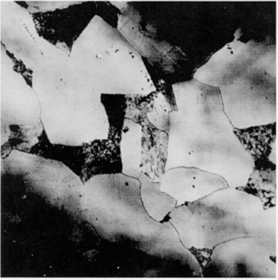
Fig. 26 SAM image at 1.3 GHz of a polished but unetched manganeze-zinc low-
carbon steel. Darker regions
indicate the presence of typical contaminants trapped in the metal.
Courtesy of G.H. Thomas, Sandia National
Laboratories
Microelectronic Components
In the field of microelectronics, reliability is affected by tiny defects that may be harbored within a component or
assembly but that are not detectable by electrical testing. The defects may grow with time or with thermal cycling, and
when they reach a critical size, electrical performance may be affected; that is, a connection may break, or an electrical
characteristic may change. Integrated circuits, ceramic capacitors, and thyristors that contain defects of this type will be
examined in this section.
Integrated Circuits (ICs). A typical silicon IC chip (die) generates heat during its normal operation. The heat must
be dissipated to stabilize the electrical behavior of the semiconductor. Therefore, the die is bonded onto a thermally
conductive substrate, such as copper, aluminum oxide, or beryllium oxide. A high-reliability IC must also be hermetically
sealed from ionic contamination and moisture in the atmosphere; therefore, a sealed ceramic or ceramic/metal package is
used to house the die and to serve as an interconnection vehicle. Figure 27 shows a typical ceramic IC package containing
a die bonded to a gold-plated surface. The die bond is also referred to as a die-attach.
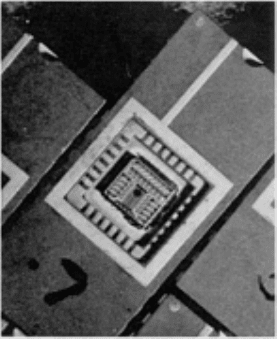
Fig. 27 Typical ceramic-packaged IC showing the silicon die, which is bonded to the metallized surface
To complete the component, tiny interconnection wires are attached from the die to the corresponding metallization sites
(bond pads) inside the ceramic package. A metal cover (lid) is then soldered to the top of the package. Apart from defects
in the silicon chip itself, the life of the component depends on the quality of the die-attach, the integrity of the
interconnection wire bonds, and the lid seal, all of which require good bonding.
Conventional Radiography Limitations. Because of its wide acceptance, conventional or x-ray radiography has
usually been the first method of investigation for virtually all internal examinations (see the article "Radiographic
Inspection" in this Volume). However, it has finally been realized that x-ray techniques indicate only the presence,
absence, and density of materials through which the beam passes. On the positive side, if a poor bond is caused by the
absence of a material, for example, solder, there will be less x-ray absorption and therefore a correct indication of a
defect. However, if all the materials are present and in their proper proportions, there can be no differential x-ray
absorption and no defect identification.
For example, suppose that the die is uniformly coated with solder but that there is no adhesion of the solder to the
substrate due to contamination of the surface or improper metallurgy. Suppose also that the solder bonds well to the die
and to the metallic layer but that for some reason the metallic layer becomes detached from the substrate. Both of these
conditions are common problems that cannot be detected by x-ray but, because of the thin interface air gaps, cause
complete reflection of ultrasound from, and no transmission of ultrasound across, the interface (Ref 17). The U.S. military
standards for the inspection of circuits now include acoustic microscopy inspection (Ref 18).
Another common situation involves a die-attach material, such as epoxy, that is not very absorptive to x-rays, as is the
typical lead tin solder alloy. If the die is bonded to a ceramic substrate that is also not very absorptive, low-energy x-rays
can be used to detect voids (but not delaminations) in the die-attach material. However, if the die is attached to a metal
substrate that absorbs x-rays, much higher energy is required for penetration. In this case, the die-attach material
absorption becomes a negligible fraction of the total absorption signal, and neither disbonds nor voids can be detected.
Advantages of Acoustic Microscopy. The die-attach can be inspected by SLAM techniques in those cases in which
ultrasound can be coupled to the top and bottom surfaces of the IC, that is, when there is no lid enclosing the package.
When the lid is on, the air gap within the die cavity precludes the transmission of ultrasound, and a reflection method,
such as C-SAM must be used. This is not true for plastic packages, for which SLAM and C-SAM can be used.
Figure 28 illustrates the SLAM inspection of an IC. Figure 29 shows a transmission SLAM image of a die-attach. The
dark zones represent little or no ultrasound transmission. A white line generated by the SLAM image analysis system
outlines the die region.
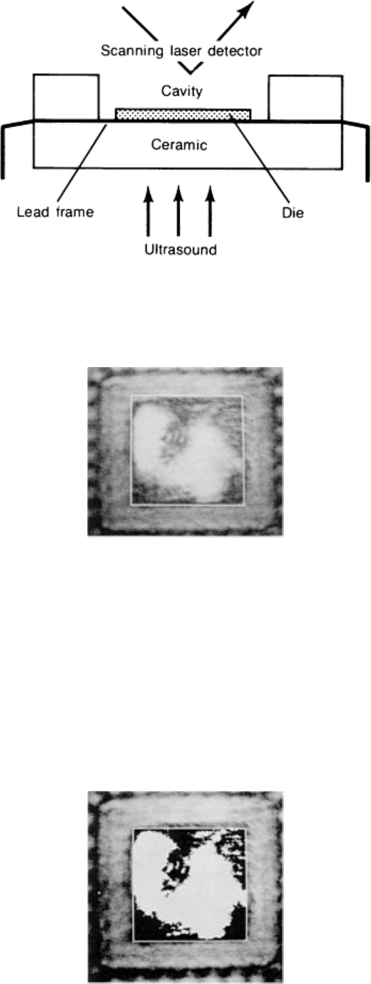
Fig. 28 Schematic illustrating use of the SLAM through transmission technique to evaluate the die-
attach bond
between the silicon die and the ceramic package
Fig. 29 30-MHz transmission SLAM image of a die-
attach. The dark areas of the image correspond to little or
no acoustic wave transmission due to the lack of bonding between the die and the ceramic. The white rectangle
outlining the die is generated by an acoustic image analysis c
omputer, which is used to determine the percent
area of disbond. A 50-MHz reflection mode C-
SAM color image of this integrated circuit is shown in Fig. 13 in
the article "Use of Color for NDE" in this Volume. Field of view: 14 × 10.5 mm
Figure 30 shows the SLAM data after digital processing to highlight the areas of bond (white) and disbond (black).
Because of its real-time imaging speed, the scanning laser acoustic microscope would be useful for quality control
inspection of the die-attach before a ceramic IC is completely assembled.
Fig. 30 Computer-analyzed SLAM acoustic image of Fig. 29
in which the disbonds are clearly displayed as

black. A 50-MHz reflection mode C-SAM color image of this IC is shown in Fig. 13 in the article
"Use of Color for
NDE" in this Volume.
Figure 31 illustrates the inspection of an IC within a closed, hermetic package by means of C-SAM. In this case, the
ultrasound accesses the die-attach interface through the ceramic substrate. Access through the lid is precluded by the air
gap. Because of the differences in acoustic impedance, Z, between the ceramic and silicon materials, an echo will be
returned from the die-attach interface in the case of a good bond or a bad bond, although the amplitudes of the echoes
may be different. The acoustic impedances of a few typical materials are listed below:
Material
Acoustic impedance,
10
6
rayl
Air, vacuum
0
Water
1.5
Plastic
2.0-3.5
Glass
15
Aluminum
17
Silicon
20
Beryllia
32
Copper
42
Alumina
21-45
Tungsten 104
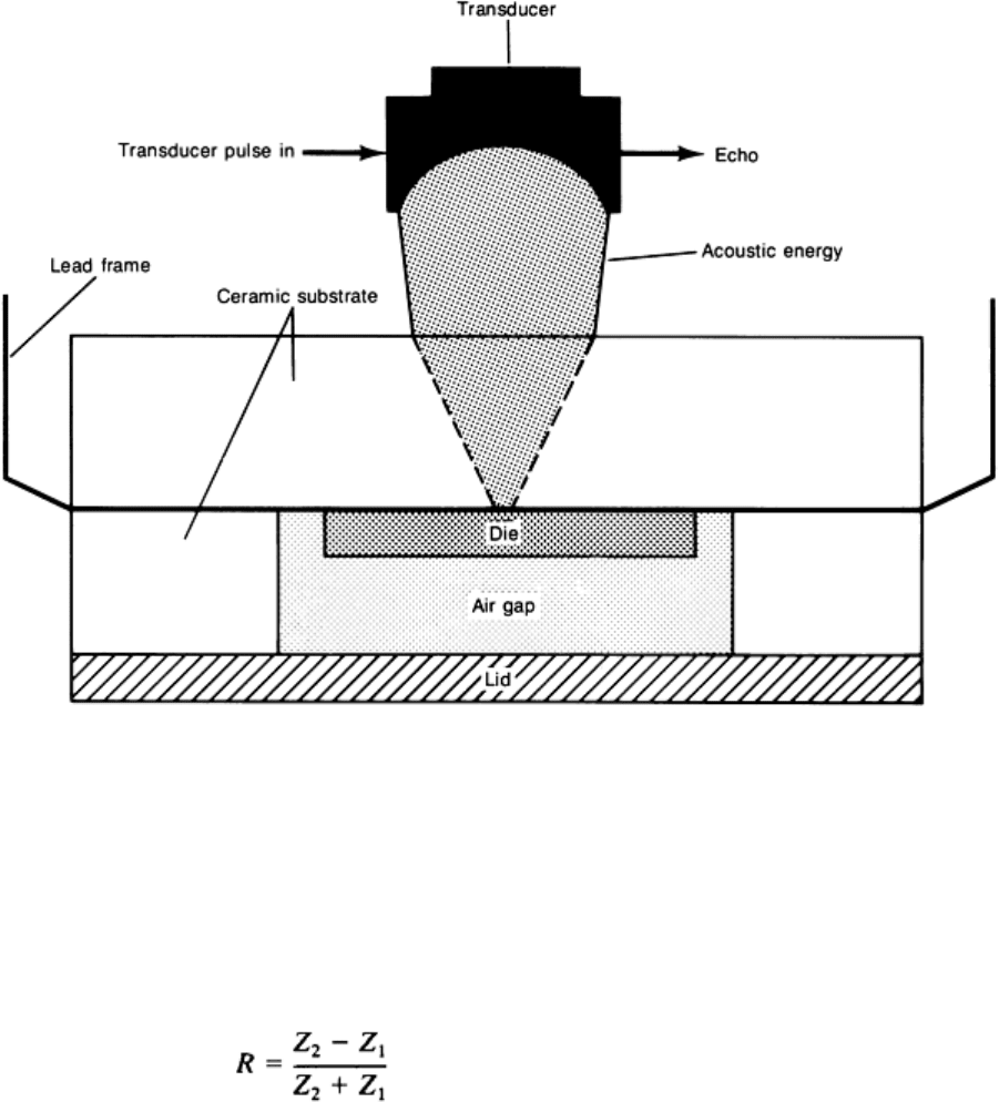
Fig. 31 Schematic illustrating use of the C-SAM reflection technique to evaluate the die-
attach bond between
the silicon die and the ceramic package of a ceramic dual-in-
line package IC. With this technique, the
ultrasound access to the bond layer is obtained by applying the pulse to the ceramic package, rather than
through the lid, to avoid the air gap over the die.
More complete information on acoustic impedances can be found in Ref 19. If the amplitude of an echo relative to the
amplitude of the incident acoustic pulse is denoted by R, then the value of R can be easily determined by the formula:
(Eq 1)
where Z
1
is the acoustic impedance of the material through which the ultrasound is traveling before reaching the interface
and Z
2
is the acoustic impedance of the material encountered on the other side of the interface. Using Eq 1 and
considering the interface materials to be alumina (Z
1
= 35) and silicon (Z
2
= 20) a good bond will have an R value of 0.27.
In the case of a complete disbands Z
2
= 0 (for air) and the R value is 1.0. In interpreting C-SAM images, because the ratio
of signal levels between good and bad will be 3.7, care must be exercised to calibrate the system on a known sample.
Fig. 13 in the article "Use of Color for NDE" in this Volume shows a reflection mode C-SAM image produced at 50 MHz
of the sample shown in Fig. 29. To assist the low-contrast differentiation of typical black-and-white gray-scale images,
the C-SAM data have been digitally processed and presented as a pseudo-color-enhanced image in which red indicates
disbond. The time gate was selected for the die-attach interface; therefore, unbonded regions of the die do not appear in
the image, because from the ceramic side, the ultrasound cannot differentiate the air gap surrounding the die from the air
gap under the disbonded areas of the die. In the case of unknown materials or in the case of not having an appropriate
calibration sample, it may be more difficult to differentiate the bond versus the nobond condition because of nearly equal
echo levels. Therefore, it is usually suggested to remove the lid from one sample of the lot and perform SLAM imaging.
With SLAM, the amplitude of signal transmission across a two-material interface, T, is governed by:
T = 1 - R
(Eq 2)
In the case of a good bond, T = 0.73, and in the case of a bad bond T = 0. The ratio of signal levels is limited only by the
dynamic range of the instrument and can be typically 1000:1. To clarify this further, the ability of any electronic
instrument to measure a zero signal level is determined by the signal-to-noise ratio of the instrument, which can typically
exceed 60 dB.
Another important issue arises in ICs when the die is encapsulated in plastic molding compound instead of a ceramic
package. In this case, both SLAM and C-SAM can be employed. When SLAM is employed, disbonds will appear
nontransmitting and therefore dark (or whichever color is assigned). However, with C-SAM, more care must be taken in
echo-level discrimination. The acoustic impedance of plastic is low (Z = 3) relative to ceramic; however, the echo
magnitude from a plastic/air interface will still be 1.0. The echo from a plastic/silicon interface, however, will be 0.75,
which is very close to 1.0, thus making the interpretation of echo level possibly difficult. Fortunately, however, the
polarity of the echoes is different for air and silicon interfaces. In the case of Z
2
> Z
1
(plastic/silicon), the echo is positive
and in the case of Z
2
< Z
1
(plastic/air), the echo is negative, according to Eq 2.
In the color-coded enhanced C-mode scanning acoustic microscope, the images can be displayed as echo-magnitude
images or as echo-magnitude and polarity images (Ref 11). This is illustrated in Fig. 32 and in the article "Use of Color
for NDE" (Fig. 12) in this Volume; both of these figures show a plastic-encapsulated IC that has disbonded areas between
the plastic molding compound and the metal lead frame. As shown in Fig. 12 in the article "Use of Color for NDE," the
color differentiation between positive echoes (blue) and negative echoes (disbond) (red) is essential for correctly
diagnosing the integrity of this device. The echo signal levels from the plastic/lead frame interface are similar to the levels
from the plastic/air gap interface; therefore, the good versus bad condition cannot be analyzed in the black-and-white
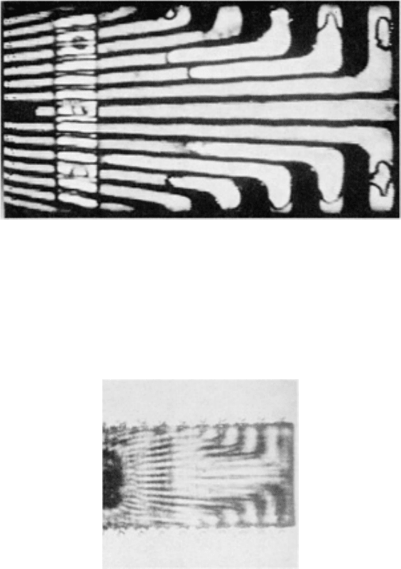
presentation of Fig. 32. A through transmission SLAM image, such as that shown in Fig. 33, is clearer with regard to
differentiating between bond (bright) and disbond (dark). A more thorough discussion of the acoustic microscopy analysis
of plastic-encapsulated ICs can be found in Ref 20.
Fig. 32 C-SAM reflection mode image at 15 MHz of a plastic-encapsulated IC showing a s
uspicious area of the
lead frame. In this image, the brightness of the image (towards white) represents the magnitude of the echoes
from the interface. There is no regard for the polarity of the echoes. The color version of this image, shown in
Fig. 12 in the article "Use of Color for NDE" in this Volume, is a dramatic improvement over the black-and-
white
image shown here and clearly differentiates the bonded regions from the unbonded regions of the lead frame.
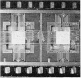
Fig. 33 SLAM through transmission image produced at 10 MHz of sample shown in Fig. 32
of this article and
Fig. 12 in the article "Use of Color for NDE"
in this Volume. In this image, the disbonded zones are presented as
dark. Careful analysis of Fig. 33 indicates that the disbonded areas in black-and-
white are larger than those
indicated in the color micrograph. This is explaine
d by the fact that the scanning laser acoustic microscope
shows the disbonds on either side of the lead frame, that is, two interfaces, while the C-
SAM image shows only
one interface. When the IC was turned over and the opposide side of the lead frame exam
ined, the SLAM and
C-SAM information agreed. Field of view: 35 × 26 mm
At this point it should be mentioned that the interpretation of echoes is not always simple. Equations 1 and 2 are restricted
to an interface of two thick materials. If there is a thin layer, echoes from the front and back surfaces of the thin layer will
merge, and the resulting pulse shape will become distorted. More detailed analysis of the echo shape will be needed to
determine the nature of the interface (Ref 21). Complete information on IC packaging is available in Ref 22.
Integrated Circuit Wire Bonding. Another problem with ICs is the connection of the tiny wires to the silicon chip.
High-speed, densely spaced ICs may contain well over 300 leads. Traditional techniques of wire bonding use 0.018 mm
(0.0007 in.) diam gold wires that are individually point-by-point stitch bonded from pads on the chip to pads on the
package. Newer methods involve gang bonding, that is, the simultaneous bonding of a network frame of leads
mechanically fixed in position by a polyimide film (tape). These are created by photo etching a pattern in a solid sheet of
0.025 mm (0.001 in.) thick copper that is bonded to the film. A sample produced by this method is shown in Fig. 34. This
process, known as tape automated bonding (TAB), may soon become a widely used method for assembling ICs of all
types.
Fig. 34
IC bonded to a frame of tiny leads that have been simultaneously bonded by a process known as tape
autom
ated bonding. This process is being used to perform interconnections on densely packed ICs having over
300 leads per chip.
In order for the process to become acceptable, however, the bond integrity of each lead must be ensured. With
conventional stitch wire bonding, each wire can be stressed up to a few grams-force in a device called a nondestructive
mode pull tester. Unfortunately, the high population density of TAB leads precludes pull testing, except in the case where
the device is destroyed to measure the quality of the lead bonds. Acoustic microscopy, particularly SLAM, was
determined to be a very reliable nondestructive test method (Ref 23, 24). The notion behind developing the test was that if
the areas of bonding of the leads could be measured and if the areas of the bonds correlated with the mechanical strength
of the bonds upon destruction, then the test method could be employed nondestructively on subsequent samples (Ref 25).
The good correlations described in Ref 23 and 24 are summarized and illustrated in the discussion that follows. Figures
35 and 36 show 200-MHz SLAM images of lead bonds on two IC chips. Some of the leads are bonded well, as indicated
by the clear, bright areas, and other leads are obviously disbonded, completely or partially. Figure 37 shows a graph in
which the area of bond, relative to a 100% maximum, is plotted for leads 1 through 68 around the perimeter of a chip.
Pull strength relative to a maximum value of 100% is also given for each lead. The pull tests were performed to the point
of failure of each lead, and the peak force was recorded. This acoustic microscopy procedure is under consideration as a
standard test method for the military.
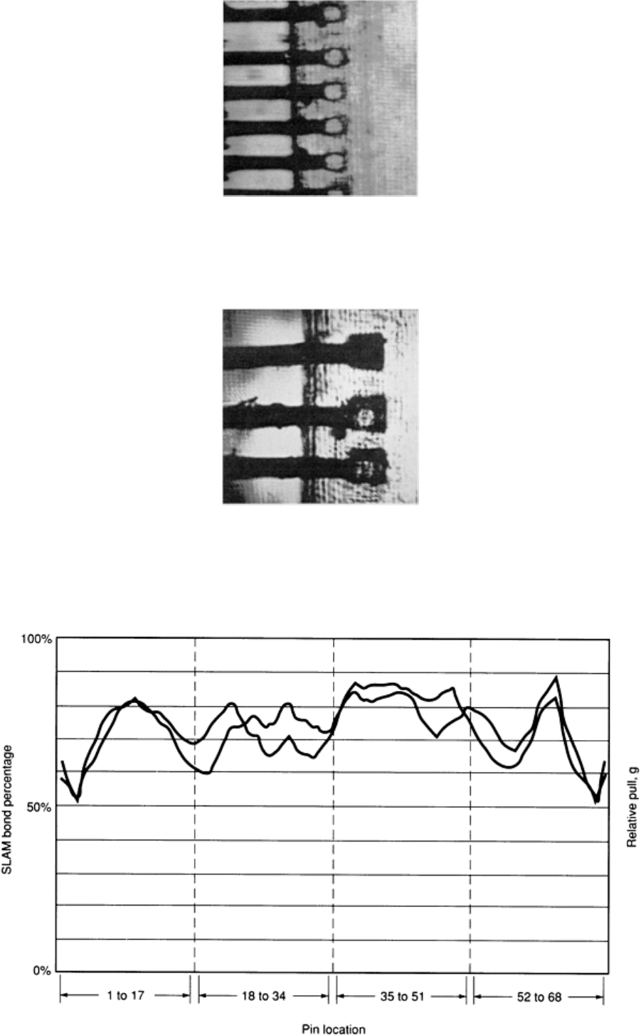
Fig. 35 SLAM acoustic image at 200 MHz of TAB-
bonded leads on an IC. The bright areas at the tips of each
lead indicate good-quality bonds. Field of view: 1.75 × 1.3 mm
Fig. 36 SLAM acoustic image at 200 MHz of TAB-bonded leads that are not of as uniform qu
ality as those
shown in Fig. 35. The poor bonds are mechanically weak and are more likely to suffer from long-term rel
iability
problems. Field of view:1.75 × 1.3 mm
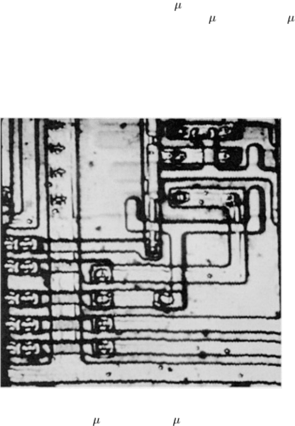
Fig. 37 Plot of bond area percentage versus pin location to verify that SLAM b
ond strength analysis agrees with
destructive pull tests. Graph shows the similarity between the relative strength of TAB-
bonded leads, as
determined by destructive pull tests, and the areas of bond, as determined by 200-
MHz SLAM, on the same
sample plotte
d as a function of location around the perimeter of an IC chip. The locations are denoted by pin
numbers 1 through 68. Pressure readings for inner lead bonding are averages obtained for numerous samples
that were tested.
Example 3: Use of SAM to Evaluate an IC on a Silicon Wafer.
Scanning acoustic microscopy offers a technique for generating high-resolution images of material structure and defects
in ICs located on silicon crystal substrates. When the IC is scanned with a scanning acoustic microscope having a 2-GHz
transducer, the image produced measures approximately 62 × 62 m (0.0025 × 0.0025 in.). This image displays the
metallization on an IC. A high-resolution, pulse-echo scan shows 4 to 6 m (160 to 240 in.) wide aluminum lines
deposited on a silicon substrate (Fig. 38). The small dark spots randomly scattered throughout the metallization are silicon
nodules, which bubble up from the substrate, creating small defects in the conducting material. Depending on the focal
depth, such structures as defects in the metallization, delaminations or disbonds between conductors, metal line thickness,
and buried p-type material can be measured or imaged. The shaded fingers midway on the right side in Fig. 38 indicate
doped material below the surface. No preparation of the sample prior to testing was necessary.
Fig. 38 Pulse-echo SAM micrograph of 4 to 6 m (160 to 240
n.) wide aluminum lines on the silicon substrate
of an IC. Dark spots are silicon nodule defects, the source of which is silicon bubbling up from the substra
te of
the wafer. Courtesy of G.H. Thomas, Sandia National Laboratories, Livermore, CA
Ceramic capacitors are passive electronic components used in virtually every electronic circuit to store electrical
charge. They are manufactured to be physically small, yet they must have very high capacitance values, which can be
obtained with specially formulated, high dielectric constant materials. Figure 39 shows various miniature multilayer
capacitors. The basic construction of a capacitor involves two parallel plate electrodes separated by a small distance that
is occupied by the dielectric. Capacitance values are inversely proportional to the dielectric thickness and are proportional
to the total area of the electrodes.
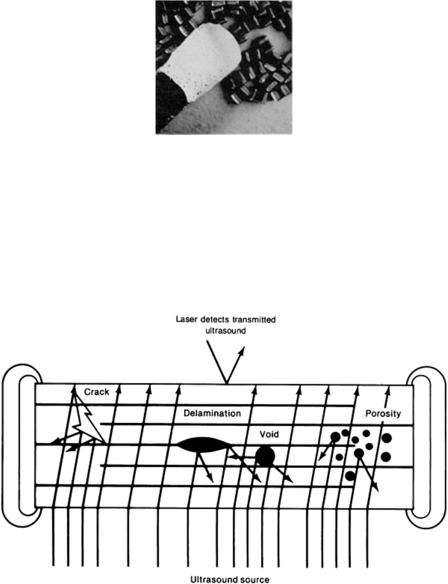
Fig. 39 Miniature ceramic capacito
rs constructed of multiple layers of high dielectric constant ceramic
alternated with layers of conductive metallization. Relative size of single capacitor is evident when compared to
the head of a match.
To increase the area in a small space, multiple layers are used and are electrically connected together in parallel. The
problems associated with capacitors that cannot be detected electrically are internal cracks in the ceramic, large voids in
the dielectric layers, delaminations between the layers, and high porosity of the dielectric ceramic material. This is
illustrated in Fig. 40. Most ceramic capacitors have barium titanate in the dielectric formulation and are therefore x-ray
opaque.
Fig. 40 Diagram illustrating the layered construction us
ed in multilayer ceramic capacitors and the locations of
potential defects in these electronic components
Ultrasound C-scan was suggested as a method for detecting flaws in ceramic capacitors (Ref 26). However, it was later
found to be useful only for the large components because of edge effects that are characteristic of all C-scan and C-SAM
images. Scanning laser acoustic microscope techniques are not necessarily limited by the edge effects, as illustrated in
Fig. 41.
