Wang Zh.M. One-Dimensional Nanostructures
Подождите немного. Документ загружается.

224 B.-K. Kim et al.
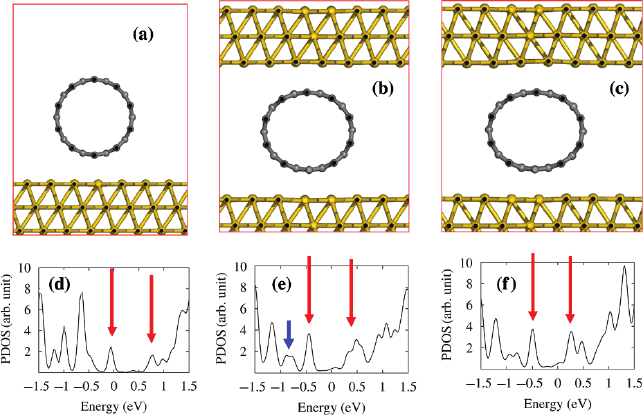
Fig. 9.5 Optimized geometries for the (10,0) carbon nanotube (a) on the Au(111) surface, and
between two gold slabs with (b) small and (c) large pressures. Panels (d), (e),and(f) show the
projected densities of states for the (10,0) carbon nanotubes for the cases of (a), (b),and(c),
respectively. Two long downward arrows in (d), (e),and(f) indicate the valence and conduction
band edges, respectively. The short downward arrow in (e) indicates the second valence band state;
the orbital characteristics of this state are depicted in Fig. 9.6
density of states (PDOS) for the nanotube are shown in Fig. 9.5. In Fig. 9.5a, only
one side of the nanotube is in contact with the gold surface. The equilibrium dis-
tance of 3.01
˚
A indicates that the nanotube is physisorbed on the surface. Since gold
has a larger work function, the Fermi level is aligned at the valence band edge of the
carbon nanotube.
To simulate the compressing metal layers, we reduced the unit cell length of
the supercell along the z-direction, as shown in Fig. 9.5b and c. The most striking
feature of Fig. 9.5b and c is that as the nanotube–metal distance is reduced, the Fermi
level shifts up, and thus becomes aligned closer to the conduction band edge of the
nanotube, as shown in Fig. 9.5f. The calculated quantum-mechanical stresses along
the z-direction are 0.61 and 6.03 kbar for Fig. 9.5b and c, respectively. The nonzero
density of states in the band gap region is due to the metal-induced gap states. It
is also noticeable that the peaks corresponding to the second van Hove singularity
are suppressed significantly when the nanotube is compressed by the gold slabs, as
indicated by the short downward arrow in Fig. 9.5e.
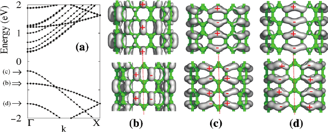
To understand these changes in the PDOS, we calculated the electronic struc-
ture of an isolated squeezed (10,0) nanotube with the same atomic geometry as in
Fig. 9.5c without the metal layers. Note that the energy gap and band dispersion
of the squeezed nanotube are almost the same as those of the pristine nanotube,
as shown in Fig. 9.6a. The isosurfaces of the three doubly-degenerate valence band
states at Γ are plotted in Fig. 9.6b, c, and d. The phase changes of the Kohn–Sham
9 Designing the Carbon Nanotube Field Effect Transistor 225
Fig. 9.6 The band structure of the isolated squeezed nanotube with the same geometry as Fig. 9.5b
without the compressing metal layers. Panels (b), (c),and(d) are contour plots of the charge density
of the three doubly degenerate states at the Γ point, as indicated by the three rightward arrows in
panel (a).The+/− signs in (b), (c),and(d) indicate the phase of the wave function. The vertical
dotted lines in (b), (c),and(d) represent the mirror reflection plane. Reused with permission from
Noejung Park, Donghoon Kang, and Suklyun Hong, Applied Physics Letters, 87, 013112 (2005).
Copyright 2005, American Institute of Physics
wave function, indicated by +/− signs, show that the second valence state changes
most slowly along the nanotube–metal contact (dotted lines). Therefore, the hy-
bridization of this state with the Au 6s bands is easier than other valence states.
This explains why the second van Hove singularity is strongly affected, as shown in
Fig. 9.5e, by the shortening of the nanotube–metal distance. As a result, the occupa-
tion of the Au 6s bands increases, which means that the amount of charge transfer
from the CNT to the gold layer is also increased. Thus the Fermi level up-shift
shown in Fig. 9.5e and f is a consequence of the lowered local potential, which is in
turn due to the increased electron depletion in the CNT region.
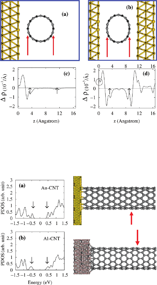
The variation in the charge transfer with the pressure can be seen explicitly in the
charge density differences, ∆
ρ
=
ρ
[CNT/M]−
ρ
[CNT]−
ρ
[M], where M is a metal
layer. ∆
ρ
was plotted along the z-direction after averaging over the xy plane. z is the
distance from the topmost gold layer, and the arrows in Fig. 9.7c and d indicate the
edges of the CNT. Figure 9.7c shows that electronic charge accumulates on the side
of the gold surface, which indicates that the electronegativity of gold is larger than
that of the CNT. The comparison of Fig. 9.7c and d shows that electron accumulation
just above the gold surface increases when the contact is under pressure. This result
is consistent with the increased Au-C hybridization, as discussed earlier. The charge
transfer induced by the hybridization largely compensates the difference between
the local work functions of gold and the CNT, pushing the Fermi level toward the
conduction edge of the CNT. We also performed a similar calculation with other
faces of gold and found similar results.
Now we turn to the case in which strong chemical bonds have formed at the
metal–CNT interface [40,59]. In Fig. 9.8, we show that the Fermi levels of both the
gold and aluminum layers are located at the midgap of the carbon nanotube when
the metal layers and the carbon nanotube are chemically bonded. This suggests that
the Fermi level of the metal is strongly pinned at the midgap of the CNT, irrespective
226 B.-K. Kim et al.
Fig. 9.7 Optimized geometries for the (10,0) carbon nanotube (a) on the Au(111) surface and (b)
between two gold slabs. The charge density differences, as defined in Fig. 9.2, for the configura-
tions (a) and (b) are plotted along the direction perpendicular to the metal surface in (c) and (d),
respectively. Two upward arrows in (a)–(d) indicate the edges of the nanotubes. Reused with per-
mission from Noejung Park, Donghoon Kang, and Suklyun Hong, Applied Physics Letters, 87,
013112 (2005). Copyright 2005, American Institute of Physics
Fig. 9.8 Electronic structures and bonding configurations of (a) Au layers and (b) Al layers in
end-contact with a semiconducting (10,0) CNT. Partial densities of states (PDOS) for 20 carbon
atoms of the CNT, which is the 9th zigzag chain from the metal surface, indicated by the red
arrows in the atomic geometries, are shown with respect to the Fermi level of each configuration.
The two downward arrows in the PDOS indicate the valence and conduction band edges. In these
calculations, the 10 nm long CNT is connected to the metal at both ends, but only one end part is
shown. Reused with permission from Sunkyoung Moon, Sun-Gul Lee, Woon Song, Joon Sung Lee,
Nam Kim, Jinhee Kim, and Noejung Park, Applied Physics Letters, 90, 092113 (2007). Copyright
2007, American Institute of Physics
9 Designing the Carbon Nanotube Field Effect Transistor 227
of the metal work function. On the basis of these results, we suggest that the micro-
scopic differences between the metal–CNT interfaces are very important influences
on the Schottky barrier. The adsorption states and bonding configurations at the
metal–CNT interface are also likely to substantially affect the transport behavior of
SWNT-FETs. This also means that engineering of the metal–CNT interface could
be exploitable to achieve SWNT-FETs with desired conduction patterns.
9.3 Metal–Carbon Nanotube Contact Engineering
In this section, we describe various experimental techniques for controlling the
height of the Schottky barrier at metal–nanotube contacts, and their effects on the
electronic transfer properties of SWNT-FETs. By controlling the Schottky barrier
height, it is possible to fabricate electronic devices such as diodes and n-type transis-
tors that are necessary for logic circuits, and the delicate modulation of the Schottky
barrier can be used to develop highly sensitive SWNT-FET based sensors.
9.3.1 Fabrication of Carbon Nanotube Diodes with Contact
Engineering
In this section, we focus on the fabrication of a SWNT device that operates as a
rectifying diode. Several research groups have fabricated SWNT-based diodes, ei-
ther by using conventional approaches such as selective doping of part of the nan-
otube, or by adopting local split gates to control the carrier concentration in the
nanotube [1, 15, 31, 60]. However, by exploiting the well-known characteristics of
the Schottky barriers of SWNT-FETs, it may be possible to construct a SWNT-based
diode simply by adjusting the Fermi-level lineup at the nanotube–metal contact.
We tested this suggestion by fabricating symmetric p-type SWNT-FETs with
high work function metals, and then converted these devices into Schottky diodes
by modifying one of the contact barriers with a self assembled monolayer (SAM)
of molecules containing a thiol group.
The SWNT-FETs used in this study were fabricated with the patterned growth
method [27b.] and conventional photolithography followed by lift-off. The sample
fabrication procedure was as follows. First, catalyst patterns were created on a heav-
ily doped p-type Si wafer with 500 nm thermal oxide by using a deep-UV mask-
aligner, and the samples were allowed to react with Fe/Mo catalyst in methanol
for 10 ∼ 30s. The samples were lifted off in boiling acetone, and washed three
times with fresh acetone and isopropanol. The samples with patterned catalyst were
then transferred to a furnace, where nanotube growth was carried out in a CH
4
and
H
2
atmosphere at 900
◦
C. The electrode patterns were fabricated with photolithog-
raphy, and 5 nm titanium and 20 nm Au were evaporated successively using ther-
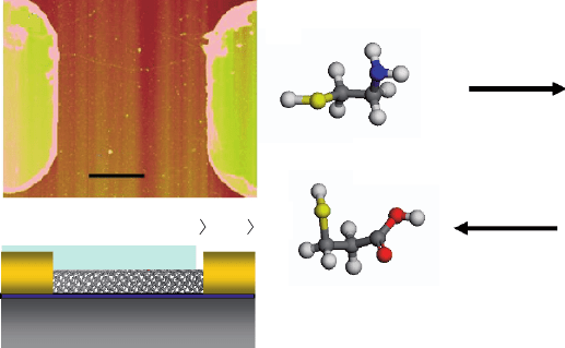
mal evaporation. Figure 9.9a shows an AFM image of the bare device used in our
228 B.-K. Kim et al.
(a) (c)
(b)
2 µm
SU-8
3-Mercaptopropionic acid
N H
2
SS
N H
2
2-Aminoethanethiol
−
−
+
+
Fig. 9.9 (a) AFM image of the device used in these experiments. (b) Schematic drawing of a
SWNT-FET with a SAM on one contact. (c) Molecular structures of the two self-assembling mole-
cules used in this study. Reused with permission from Byoung-Kye Kim, Ju-Jin Kim, Hye-Mi So,
Ki-Jeong Kong, Hyunju Chang, Jeong-O Lee, and Noejung Park, Applied Physics Letters, 89,
243115 (2006). Copyright 2006, American Institute of Physics
experiments (i.e., before SAM treatment). Patterns were created on this bare device
with an SU-8 negative photoresist to expose one of the contacts for chemical treat-
ment, as depicted in Fig. 9.9b. Two self-assembling molecules, 2-aminoethanethiol
(HSCH
2
CH
2
NH; Mw 77.15), and 3-mercaptopropionic acid (HSCH
2
CH
2
CO
2
H;
Mw 106.14) were purchased from Sigma-Aldrich, and used without further treat-
ment. These molecules were selected because they each contain a thiol group, which
is well known to favor the formation of highly ordered monolayers on Au sur-
faces [54a.]. Figure 9.9c shows the molecular structures of 2-aminoethanethiol and
3-mercaptopropionic acid, and the predicted directions of the dipole moments of the
pristine molecules.
The electrical transport characteristics of the devices were recorded prior to
molecular treatment, and then the devices were reacted with a 10 mM solution of
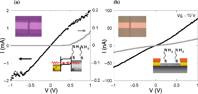
self assembling molecules in ethanol. Figure 9.10 shows the I–V characteristics of
the SWNT-FET before (black curve) and after treatment of the exposed contact
with 2-aminoethanethiol (gray curve; reaction time of 10 min). The upper left inset
shows an optical microscopy image of the device, and the lower right inset shows
the band diagram after the 2-aminoethanethiol treatment. As shown in Fig. 9.10a,
a symmetric I–V curve was observed before introduction of the SAM. After the
2-aminoethanethiol treatment, in contrast, the device exhibits highly asymmetric,
diode-like I–V characteristics.
For comparison, we fabricated a device in which both contact electrodes were
covered with SU-8, exposing only the nanotube body region. After treatment of
these SU-8-covered electrodes with 2-aminoethanethiol, the device was found to ex-
hibit symmetric I–V characteristics with decreased conductance (Fig. 9.10b). This
result is consistent with those of Kong et al., who attributed this conductance de-
crease to the electron doping nature of the amine groups [26]. When we used a
3-mercaptopropionic acid SAM in similar experiments, no significant changes in
the transport characteristics were observed (data not shown).
9 Designing the Carbon Nanotube Field Effect Transistor 229
Fig. 9.10 (a) I–V curves measured before (black, at V
g
= 0) and after treatment of the surface
with 2-aminoethanethiol (gray curve). Upper inset: optical microscopy image of the single-contact
open device. Lower inset: schematic band diagram of the device. (b) I–V curves before (black) and
after (gray) 2-aminoethanethiol treatment of the contact-passivated device. Reused with permission
from Byoung-Kye Kim, Ju-Jin Kim, Hye-Mi So, Ki-Jeong Kong, Hyunju Chang, Jeong-O Lee, and
Noejung Park, Applied Physics Letters, 89, 243115 (2006). Copyright 2006, American Institute of
Physics
The diode-like operation of the SWNT-FET with a 2-aminoethanethiol SAM can
be explained by the formation of asymmetric contacts after the molecular treatment
of the cathode surface, as depicted in the inset in Fig. 9.10a. To fabricate the Schot-
tky diode, we used a self assembly technique to adjust the Fermi-level lineup of the
predefined nanotube transistor. A similar self assembly approach has been used to
control the Schottky barrier height in organic electronic devices. [7, 10] For com-
parison, we used two molecules, 2-aminoethanethiol and 3-mercaptopropionic acid,
which were expected to have different dipole directions (see Fig. 9.9c). We found
that only treatment with 2-aminoethanethiol resulted in diode-like operation.
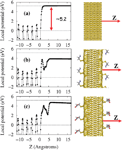
We investigated the different effects of adding the 2-aminoethanethiol and
3-mercaptopropionic acid molecules to a bare Au surface by carrying out ab initio
electronic structure calculations. We used the calculation method described in our
previous study [41a.]. Here we adopted a slab geometry with six gold layers, in
which the two layers in the center were fixed during the geometry optimization
calculation. Plotting the local potential with respect to the Fermi level, we obtained
the work function of the bare Au surface and of the Au surfaces with adsorbed
2-aminoethanethiol and 3-mercaptopropionic acid, as shown in Figs. 9.11a, as well
as 11b, and c, respectively. The calculated work function of the bare Au surface
(≈5.2eV) is very close to the previously reported value [36]. The work functions
of the Au surfaces with adsorbed 2-aminoethanethiol and 3-mercaptopropionic
acid (Fig. 9.11b and c) are significantly different. Specifically, the adsorption of
2-aminoethanethiol molecules substantially decreases the work function (≈3.9eV),
whereas the adsorption of 3-mercaptopropionic acid has little effect (≈4.7eV).This
difference confirms that the asymmetric I–V pattern observed after treatment of one
230 B.-K. Kim et al.
Fig. 9.11 Plots of the local potentials with respect to the Fermi level of (a) thebare6layersofAu,
(b) the 6 layers of Au with adsorbed 2-aminoethanethiol molecules, and (c) the 6 Au layers with
adsorbed 3-mercaptopropionic acid molecules. Reused with permission from Byoung-Kye Kim,
Ju-Jin Kim, Hye-Mi So, Ki-Jeong Kong, Hyunju Chang, Jeong-O Lee, and Noejung Park, Applied
Physics Letters, 89, 243115 (2006). Copyright 2006, American Institute of Physics
electrode of the SWNT-FET with 2-aminoethanethiol was due to a change in the
Schottky barrier at the treated contact.
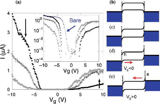
To investigate the effect on the transfer characteristics of treatment with
2-aminoethanethiol, we measured the evolution of the I–V
g
characteristics of the
SWNT-FETs, as shown in Fig. 9.12a. Before the reaction with 2-aminoethanethiol,
the device exhibits typical p-type transistor behavior (black circles). After treat-
ment with 2-aminoethanethiol for 10 min (empty squares) and 5 h (gray symbols),
however, the p-channel conduction decreases and n-type conduction becomes
dominant, as indicated by the solid arrows in Fig. 9.12a. The effect of adding the
2-aminoethanethiol SAM seems to saturate after a reaction time of about 5 h, with
the I–V
g
characteristics remaining almost unchanged upon further treatment. As
a result, the SWNT-FET with a 2-aminoethanethiol SAM on one contact exhibits
ambipolar transfer characteristics.
The ambipolar transfer characteristics can be explained by considering the band
diagram for a device with asymmetric contacts, as generated by SAM treatment of
one contact. Before the SAM treatment (Fig. 9.12b), the Fermi levels of the elec-
trodes are aligned with the valence band of the carbon nanotube, leading to p-type
behavior. After the formation of the 2-aminoethanethiol SAM (Fig. 9.12c), how-
ever, the Fermi level of the cathode is aligned with the conduction band edge. For
9 Designing the Carbon Nanotube Field Effect Transistor 231
Fig. 9.12 (a) The evolution of the electrical transfer characteristics with the formation of a
2-aminoethanethiol SAM: before reaction (black circles); after 10 minutes of reaction (empty
squares); and after 5 h of reaction (gray squares). The inset shows a log-scale plot. The band
diagram of the SWNT-FET (b) before and (c) after SAM treatment. The band diagram of the
SWNT-FET with one contact modified for (d)V
g
< 0and(e) V
g
> 0. Reused with permission from
Byoung-Kye Kim, Ju-Jin Kim, Hye-Mi So, Ki-Jeong Kong, Hyunju Chang, Jeong-O Lee, and
Noejung Park, Applied Physics Letters, 89, 243115 (2006). Copyright 2006, American Institute
of Physics
a SWNT-FET with a SAM-modified electrode, the hole current would still dominate
when V
g
< 0, as shown in Fig. 9.12d. However, significant electron conduction will
occur in the SAM-modified device when V
g
> 0, as shown in Fig. 9.12e. As a result,
the device exhibits ambipolar transfer characteristics.
It is also noteworthy that the threshold voltage of the device does not change
significantly after the SAM treatment of one of the contact electrodes, as shown
in Fig. 9.12a. It is well known that shifts in the threshold voltage are largely due
to variations in the doping level in the semiconductor channel region, whereas
changes in the slope of I–V
g
curves are due to variations in the Schottky barrier
at the contact [12]. As shown in Fig. 9.12a, the 2-aminoethanethiol treatment in-
duces slope changes in the I–V
g
curve, eventually resulting in ambipolar behavior,
with no prominent shifts in the threshold voltage. These findings confirm that the
introduction of the 2-aminoethanethiol SAM modifies the Schottky barrier at the
engineered contact.
In summary, we have fabricated a p-type SWNT-FETs and then converted it into a
diode bytuning the Schottkybarrier height using a SAM technique. Highly asymmet-
ric, diode-like I–V curves were observed when one of the contacts was functionalized
with a 2-aminoethanethiol SAM. Ab initio electronic structure calculations con-
firmed that the adsorption of 2-aminoethanethiol onto an Au surface induces a strong
decrease in the work function, whereas the adsorption of 3-mercaptopropionic acid
has little effect. These results indicate that tuning the Schottky barrier by introducing
a SAM of a selected molecular species could be a practical method to control the
conduction patterns of nanotube-based electronic devices.
232 B.-K. Kim et al.
9.3.2 Fabrication of n-Type Single-Walled Carbon Nanotube
Transistors with Al Decoration
In this section, we discuss the fabrication of n-type SWNT-FETs using a controlled
in situ Al decoration technique. By using the Al decoration technique, Schottky
barrier control and channel doping are possible at the same time, and it is possible
to compare the effects of channel doping with those of contact-barrier control.
The same sample fabrication process as described in the previous section was
used. Bare SWNT-FETs (open devices) were prepared, and contact-decorated
SWNT-FETs or channel-decorated SWNT-FETs were prepared by using an SU8-
2002 negative photoresist or a PMMA mask.
For the in situ electrical measurements, the samples were wired to a chip con-
nected to electrical feedthrough in an evaporation chamber. For Al decoration, the
vacuum chamber was pumped down to 2 ×10
−6
torr, and the Al source was slowly
evaporated by using an electron beam while monitoring the conductance of the
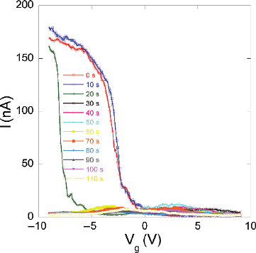
SWNT-FETs. Figure 9.13 shows the variation of the electronic transfer character-
istics of the SWNT-FETs with controlled Al deposition. Upon Al deposition, the
electronic transfer curves shift toward more negative gate voltages. The curves
were obtained by carrying out measurements every 10 s: it can be seen that p-
type conduction disappears completely after about 30 s. The deposition rate was
carefully kept below 0.1
˚
A/s. After about 2–4 min deposition, the p-type SWNT-
FETs were converted into n-type SWNT-FETs. Figure 9.14 shows the changes in
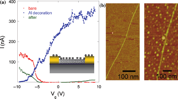
the electronic transfer characteristics and AFM images of an open SWNT-FET. For
this sample, about 30
˚
A thick Al was deposited while monitoring the conductance.
As shown in Fig. 9.14a, the sample exhibits enhanced n-type conduction follow-
ing the Al deposition. The doping level of the Al-decorated n-type SWNT-FET
Fig. 9.13 The changes in the electronic transfer properties of an open SWNT-FET resulting from
in situ Al decoration
9 Designing the Carbon Nanotube Field Effect Transistor 233
Fig. 9.14 (a) The changes in the electronic transfer properties of the device resulting from Al dec-
oration. (b) AFM images of the device. Reused with permission from Hyo-Suk Kim, Byoung-Kye
Kim, Ju-Jin Kim, Jeong-O Lee, and Noejung Park, Applied Physics Letters, 91, 153113 (2007).
Copyright 2007, American Institute of Physics
can be controlled by varying the Al deposition time. In this particular device, the
on/off ratio of the n transistor is about 10
3
, and channel pinch off does not occur
until V
g
= −10V. Upon adsorption of Al onto the carbon nanotube, electrons will
be transferred from Al to the carbon nanotube, since Al has a lower work func-
tion (4.1 eV) than the nanotube (4.8 eV). Further, the presence of Al clusters in the
contact region can lower the height of the Schottky barrier to electron transport.
However, the device gradually became a p-type SWNT-FET again when exposed to
air. Such phenomena are attributed to the oxidation of Al and the subsequent work
function increase, as indicated by electronic structure calculations in Sect. 9.2.1.
Similar behavior was observed for the contact-decorated and channel-decorated
devices; the devices become n-type transistors after decoration, and are gradually
converted back to p-transistors in air. Channel-decorated devices exhibit decreased
conductance after Al decoration, whereas improved transistor performance was
observed in the contact-decorated devices. The controlled deposition of metallic
nanoparticles can thus be an effective method for the fabrication of complementary
SWNT-FETs and highly sensitive sensor devices, though care must be taken not to
introduce oxygen into the system.
9.3.3 The Effects of Metal Clusters on Carbon Nanotube Sensors
In the previous section, we showed that it is possible to fabricate n-type nanotube
transistors by decorating low work function metals onto nanotubes. In this section,
we discuss the effects of the decorated metal particles on the sensing characteris-
tics of SWNT-FET based chemical sensors and how the change in work function
affects them.
