Wang Zh.M. One-Dimensional Nanostructures
Подождите немного. Документ загружается.

12 Ordering of Self-Assembled Quantum Wires on InP(001) Surfaces 295
are well alternate bright/dark contrast regions in the InAlAs layer. These contrast
regions are oriented along the [1
10] direction and are not very uniform in width,
with a contrast modulation wavelength ranging from 45 to 130 nm. Energy disper-
sive X-ray spectrometry (EDX) is performed to study the origination of this contrast.
According to the In atom content obtained from the EDX measurements, the In com-
position ranges are calculated to be 0.5–0.53 in the darker regions and 0.46–0.48 in
the brighter regions. These alternate In-rich and In-poor (Al-rich) bands reveal that
the LCM phenomenon has actually occurred in the InAlAs epilayer grown on InP
substrate. On the surface of such composition-modulated InAlAs layer, the tensile
strain and compressive strain in the In-rich and Al-rich regions will also lead to
morphology undulations on the sample surface [10], which has been evidenced by
in situ reflection high energy electron diffraction (RHEED) observations. After the
deposition of 500 nm-thick InAlAs layer, the RHEED patterns are V-shaped spots
along the [1
10] direction and the superposition of streaks and spots along the [110]
direction. The different RHEED patterns indicate the appearance of an elongated
structure along the [1
10] direction on the InAlAs surface [11]. Figure 12.3 presents
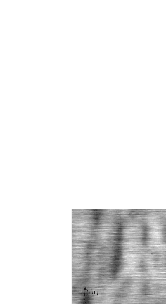
a typical AFM image of the InAlAs surface, which shows obvious morphology un-
dulations aligned along the [110] direction. The undulations are not very uniform,
and some undulations might coalesce or bifurcate. The undulation wavelength ob-
tained from the AFM images ranges from 50 to 140 nm, which is approximate to
the modulation wavelength obtained from the TEM measurements.
This LCM effect in InAlAs layer is further confirmed by the optical mea-
surements of the InAs/InAlAs/InP QWR samples. As shown by S. Francoeur et
al. [12, 13], an important result from LCM in InAlAs layer is the in-plane opti-
cal anisotropy between [110] and [1
10] in the vicinity of the band gap. Here, re-
flectance difference spectroscopy (RDS) is taken to measure the reflectance differ-
ence of InAlAs epilayers along two perpendicular directions ([110] and [1
10]) in
the surface plane, i.e., (r
110
−r
110
)/(r
110
+ r
110
) [14], where r
110
and r
110
denote
the reflectance for light polarized along the [110] and [1
10] directions, respectively.
Fig. 12.3 AFM image of an
InAlAs surface without InAs
deposition. The size of the
image is 0.5µm ×0.5µm
296 W. Lei et al.
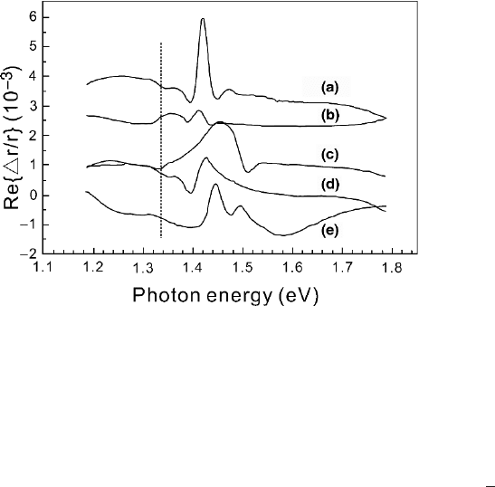
Fig. 12.4 RD spectra of the InAlAs layers measured at room temperature. Spectra (a)–(e)corre-
spond to InAlAs layer of the samples sequentially shown in Fig.12.1(a)–(e)
The RDS results measured at room temperature are shown in Fig. 12.4. Strong res-
onant structures are observed between 1.38 and 1.52 eV, which can be attributed
to the InAlAs band gap. There is also a weak resonant structure at 1.34 eV, indi-
cated by a dashed line, which can be related to the InP band gap. It is known that
Cu–Pt ordering can also cause the optical anisotropy between the [110] and [1
10]
directions [15,16]. However, TEM and electron diffraction measurements show that
there is no Cu–Pt ordering in these InAlAs samples. Therefore, the observed optical
anisotropy mainly comes from the LCM effect in InAlAs layers. In the meantime,
from AFM and RDS measurements of the samples grown under different growth
conditions, a close correlation between the RD intensity of InAlAs and the mor-
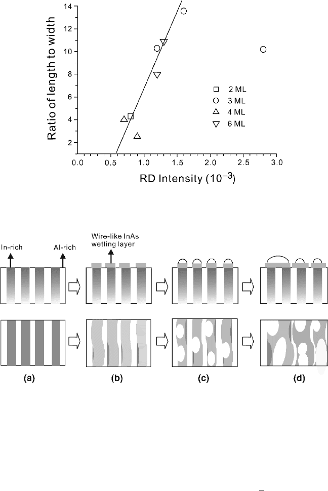
phology parameters of InAs nanostructures is established. Figure 12.5 illustrates the
ratio of the length to the width of the InAs wire-like structures as a function of the
RD intensity of InAlAs layers. Obviously, strong RD intensity of InAlAs layer cor-
responds to elongated shape of the InAs nanostructures. Because the RD signal is
related to the LCM effect in InAlAs layer, this result reveals that the formation of
wire-like islands on InAlAs surfaces is related to the LCM effect in InAlAs layers.
Because of the smaller misfit strain energy [10], the regions with tensile strain
on the surface of InAlAs layer will provide the preferential nucleation sites for InAs
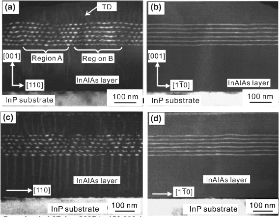
nanostructures. From this point of view, a modified SK growth mode is proposed,
as shown in Fig. 12.6. First, at the initial stage of InAs deposition, wire-like wetting
layers, instead of a planar wetting layer covering the whole substrate surface, are
formed on the In-rich regions. The sizes of the wetting layers might not be uniform
because of the nonuniformity of the composition modulation. Then, as more InAs
is deposited, the accumulated elastic strain in the wire-like wetting layer becomes
strong. SK transition will occur on the wire-like wetting layer forming QDs to re-
lax the excess strain. Meanwhile, the number of QDs will increase with increasing
InAs layer thickness. Finally, if the InAs coverage goes on increasing, the initial
12 Ordering of Self-Assembled Quantum Wires on InP(001) Surfaces 297
Fig. 12.5 The ratio of the length to the width of the InAs wire-like structures formed under vari-
ant InAs deposition thickness as a function of the RD intensity of InAlAs layer underlying the
corresponding InAs layer
Fig. 12.6 Schematic diagram of the modified SK growth mode that occurs on a composition mod-
ulation surface: (a) composition-modulated InAlAs layer, (b) wire-like InAs wetting layer formed
on top of the In-rich areas, (c) elongated QDs formed on the wire-like InAs wetting layer, (d)co-
alescence of wire-like wetting layer and QDs respectively. The first row is the cross-section view;
the second row is the top view
formed wire-like wetting layer might coalesce and become wider, thus its lateral
domination on the QDs is weakened. Here, the newly created QDs on the wider
wire-like wetting layer might not be strictly aligned along the [1
10] direction. The
coalescence of QDs with different orientation on the wires leads to formation of
larger and longer dots with irregular shape. This modified SK growth mode is en-
ergy favorable if the growth occurs on a composition-modulated layer. In this case,
the pitch period
λ
of the wire-like wetting layer is expected to approximately equal
298 W. Lei et al.
to the modulation wavelength of the InAlAs layer. However, it is noted that the
nonuniform strain distribution of LCM will also lead to a surface undulation, which
is indeed observed in our experiments. It is believed that composition modulation
can couple with a surface undulation with identical wavelength or one half wave-
length [17]. The combined effect of the LCM and surface undulation will probably
lead to the formation of InAs QWR with the pitch period
λ
to be one half of the
wavelength of the LCM. That is probably the reason for the discrepancy between
the
λ
value of the InAs QWRs, about 25 nm for all samples, and the wavelength of
LCM ranging from 45 to 130 nm.
This modified SK growth mode is further confirmed by the growth of InAs
nanostructures on InAlAs layers with strengthened and weakened LCM effect in
it [18, 19]. Figure 12.7 shows the [1
¯
10] and [110] cross-sectional dark-field (DF)
TEM images of InAs/InAlAs nanostructures grown on normal and misoriented (8
◦
off (001) toward (111)) InP(001) substrates [18]. The samples are composed of
a 300 nm-In
0.5
Al
0.5
As buffer layer, six periods of 4 ML-InAs/15 nm-In
0.5
Al
0.5
As
and an 80 nm-In
0.5
Al
0.5
As cap layer. Both the DF TEM images are obtained with
g = 002 reflection, which is more sensitive to composition than strain. So, the con-
trast is mainly attributed to the composition difference. The bright and dark regions
in InAlAs buffer layers in Fig. 12.7 correspond to In-rich and Al-rich regions, re-
spectively. As shown in Fig.12.7a, there are some LCM effect existed in the InAlAs
buffer layer, which leads to the formation of InAs QWRs in the sample. However, it
is observed that the LCM effect in the InAlAs buffer layer grown on the misoriented
Fig. 12.7 g = 002 dark-field [1
¯
10] and [110] cross-sectional TEM images for the sample grown on
normal InP(001) ((a)and(b)) and misoriented InP(001) substrate ((c)and(d)). Note that within
the epilayer in Fig. 12.7(a), threading dislocation (TD) is visible as indicated by the arrow
12 Ordering of Self-Assembled Quantum Wires on InP(001) Surfaces 299
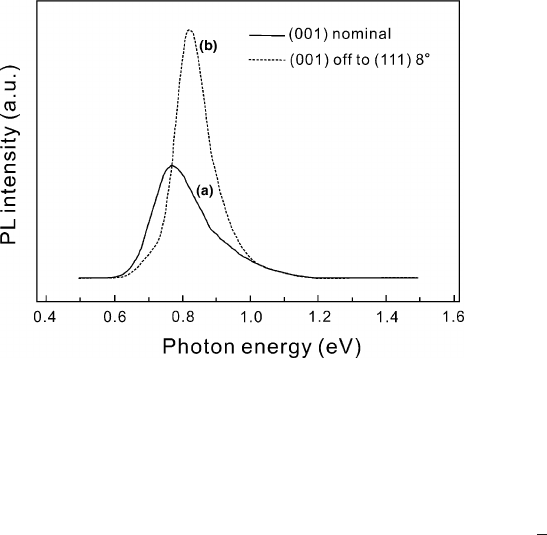
Fig. 12.8 The 77K PL spectra of the as-grown samples. Curves (a)and(b) correspond to the
samples grown on the normal and misoriented InP(001), respectively
InP substrate is greatly strengthened. As shown in Fig. 12.7c, well alternate In-rich
and Al-rich bands are developed in the InAlAs buffer layer. This reveals that obvi-
ous LCM along the [110] direction has occurred in the InAlAs buffer layer. These
In-rich bands are perpendicular to the growth surface and extend along the [1
10]
direction. The width and period of these In-rich bands are about 10 and 40 nm, re-
spectively. The origin of this strong LCM effect in the InAlAs buffer layer can be
mainly attributed to the bunching of surface steps, which has been discussed by
Wang et al. [18]. Because of the small misfit-energy, the In-rich bands will provide
the preferential nucleation sites for InAs nanostructures. So, these well alternate In-
rich and Al-rich regions provide a good growth template for the InAs nanostructures,
which greatly reduces the random nature of SK growth model and leads to a very
homogeneous size distribution for InAs QWRs. Figure 12.8 shows the 77 K photo-
luminescence (PL) spectra of InAs QWRs grown on the nominal and misoriented
InP(001) substrates. And, the full widths at half maximum (FWHMs) of the PL
spectra are 182 and 123 meV for InAs QWRs grown on the nominal and misori-
ented InP substrates, respectively. The small PL FWHM of InAs QWRs grown on
the misoriented InP substrate indicates a homogeneous size distribution for InAs
QWRs, which further confirms the important role of the LCM in InAlAs layer. In
addition, the linear density of the second-period InAs QWRs is approximately two
times of that of the first-period InAs QWRs, which is mainly induced by the very
large lateral period of In-rich bands in InAlAs buffer layer. Usually, because of
the small misfit strain energy the meeting point of the V-like In-rich arms in In-
AlAs spacer layers will provide preferential nucleation sites for the InAs QWRs in
the subsequent layer. For the certain angle (∼61
◦
) between the In-rich arms and
the (001) surface here, the V-like In-rich arms in InAlAs spacer layer originated
from the first-period InAs QWRs will meet about 30 nm above the first-period InAs
300 W. Lei et al.
QWRs because of the larger lateral period of In-rich bands in the InAlAs buffer
layer (∼33nm). So, if the InAlAs spacer layer thickness were 30 nm, the density
of the second-period InAs QWRs would be the same as that of the first-period InAs
QWRs. However, because the InAlAs spacer layer thickness here is only 15 nm, the
V-like In-rich arms in InAlAs spacer layer will not meet on the surface of the first-
period InAlAs spacer layer. Like the meeting point of the V-like In-rich arms, the
unmet In-rich arms in the InAlAs spacer layer will also provide preferential sites for
InAs QWRs in the next layer, resulting in the double density for the second period
InAs QWRs.
In the meantime, the LCM effect in InAlAs layer can also be weakened by
growing As-pressure-modulated (As-rich and As-poor) InAlAs multilayer structure
(AM-InAlAs-MLS) [19]. The structure and growth details of the sample investi-
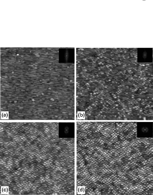
gated have been reported elsewhere [19]. Figure 12.9 shows the AFM images of
the InAs nanostructures grown on InAlAs buffer layers with different periods of
AM-InAlAs-MLS. As shown in Fig.12.9a, InAs QWRs along the [1
10] direction
are formed on conventional InAlAs buffer layer. When two periods of AM-InAlAs-
MLS are inserted before the InAs deposition, InAs QWRs and some QDs were
obtained, as shown in Fig. 12.9b. As show in Fig. 12.9c, the introduction of four-
period AM-InAlAs-MLS leads to the formation of elliptical dots elongated along
Fig. 12.9 1µm ×1µm AFM images of InAs nanostructures grown on AM–InAlAs multilayer
structures with the period number of (a)0,(b)2,(c)4,(d) 6. The insets show the Fourier transform
spectra of AFM images

12 Ordering of Self-Assembled Quantum Wires on InP(001) Surfaces 301
the [110] direction, with the average lateral size and height of the dots being 32.4 and
4.18 nm, respectively, and the density being 9.21×10
10
cm
−2
. In Fig. 12.9d, the use
of six period AM-InAlAs-MLS produces circular InAs QDs, the average width and
height of the InAs QDs being 30.5 and 3.77nm, and the density of the QDs being
about 1.16×10
11
cm
−2
. It is obvious that, with increasing the AM-InAlAs-MLS pe-
riod number, the morphology of the InAs nanostructures changes from QWRs into
mixed nanostructures including QDs and QWRs, then elliptical QDs, and finally
circular QDs. Meanwhile, the nanostructure size becomes smaller and their density
gets higher. These results reveal that the As-lacking InAlAs layers can suppress the
formation of wire-like nanostructures and favor the formation of high-density InAs
QDs. Then, what leads to this interesting experimental phenomenon? An important
factor, LCM effect, should be considered. As discussed earlier, the LCM effect in
InAlAs layer can cause the morphological undulations and anisotropic strain field on
the surface of InAlAs layer [20, 21], which could lead to the transition from QWRs
into QDs. As shown by Priester et al. [22], the phase separation can be affected by
the surface ridges of the buffer layer. The InAlAs layers grown under normal As-rich
conditions by MBE have a surface with (2×4) reconstruction [23]. And, the InAlAs
surface contains As dimers and tiny ridges aligned along the [1
10] direction [9],
which will induce the LCM in InAlAs layer with In-rich regions oriented along the
[1
10] direction. So, When InAs layer is deposited, In adatoms diffuse preferentially
along the [1
10] direction and InAs QWRs are formed [9], which is demonstrated
in Fig. 12.9a. However, the InAlAs layers grown under As-poor conditions show a
surface with (4 ×2) reconstruction [23]. This (4 ×2) surface reconstruction will
create As dimers [24] and surface ridges [25, 26] along the [110] direction, which
will result in a morphology undulation and strain field along the [110] direction. As
a result, on (4×2) reconstructed surface, the InAs islands will prefer nucleation and
growth along the [110] direction. Hence, by inserting several AM-InAlAs-MLS lay-
ers before the deposition of InAs layers, one can balance the effect of the two kinds
of surface reconstruction ((2×4) and (4×2)), which leads to the formation of InAs
QDs. In our case, with increasing the number of AM-InAlAs-MLS period, when the
effect of the As-lacking InAlAs layers is strong enough compared with that caused
by the As-rich InAlAs layers, InAs QDs are obtained, as shown in Fig.12.9c.
All the earlier-mentioned experimental results and analysis demonstrate that the
LCM in InAlAs layers plays a very important role in the formation of InAs/InAlAs
nanostructures on InP(001) substrate, which further confirms the modified SK
growth mode proposed.
12.3 Spatial Correlation of InAs Quantum Wire Superlattices
For practical device applications, vertical stacking of layers containing nanostruc-
tures (nanostructure superlattices) is usually used instead of single layer nanostruc-
tures. For nanostructure superlattices, the spatial correlation of the nanostructures
is very important, which may influence their structural, optical, and electrical
properties.
302 W. Lei et al.
12.3.1 Vertical Anticorrelation of InAs Quantum Wire
Superlattices
For InAs/GaAs QDs system [27], InAs QD superlattices demonstrate vertical cor-
relation, as shown in Fig. 12.10. This vertical correlation of InAs/GaAs QD super-
lattices can be explained by elastic strain field distribution on the surface of spacer
layers [27,28].
However, InAs/InAlAs QWR superlattices show a special spatial correla-
tion, which is completely different from that of InAs/GaAs QD superlattices.
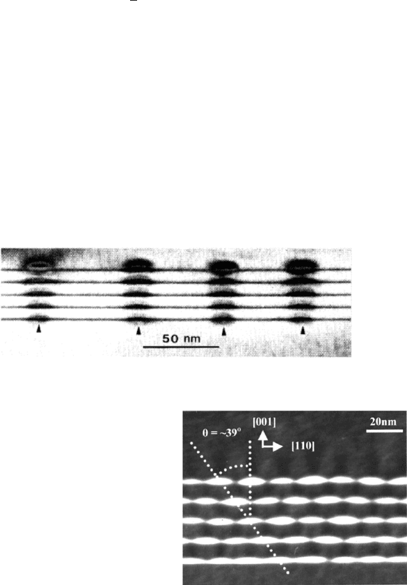
Figure 12.11 shows the typical [1
10] cross-sectional TEM images of a sample with
InAs/In
0.52
Al
0.48
As QWR superlattices grown on InP(001) substrate [29]. It is
observed that InAs QWRs are diagonally aligned along the [001] growth direction
in the InAs/InAlAs QWR superlattices. InAs QWRs in the upper layer are centered
in the interstice of QWRs of previous layer, which forms so-called “vertical anti-
correlation” [30, 31]. From the point of experiments, this vertical anticorrelation is
caused by the LCM in InAlAs spacer layer. As shown in Fig.12.11, there is obvious
LCM effect in the InAlAs spacer layers. The LCM in the InAlAs spacer layers
forms V-like In-rich InAlAs arms above the QWRs, which has also been observed
in other researches [5, 18]. The meeting points of these V-like In-rich arms will
provide adequate nucleation sites for new InAs QWRs in the next plane of stacked
structure, taking into account the smaller misfit strain energy, leading to the vertical
anti-correlation of QWR superlattices.
Fig. 12.10 Typical g = 200 dark-field cross-sectional TEM images of a sample with five sets of
InAs QDs separated by 36 ML GaAs spacer layer
Fig. 12.11 Typical g = 002
dark-field [1
¯
10] cross-
sectional TEM image of a
sample with InAs/InAlAs
QWR superlattices grown on
InP (001) substrate
12 Ordering of Self-Assembled Quantum Wires on InP(001) Surfaces 303
Theoretically, such vertical anticorrelation in InAs/InAlAs QWR superlattices
may be explained with numerically calculation of the strain distribution around an
InAs wire using finite element method based on a simple model [30]. From the
cross-sectional TEM images shown in Fig. 12.11, it can be seen that the width-to-
height ration of the InAs wire can be around 3–5 or even larger, and its effect on
strain distribution may be similar to that produced by an elastically strained ribbon
in far regions in the matrix. Therefore, in the calculation, the wire section is approx-
imated with a line segment of L
0
in original length in an isotropic two-dimensional
matrix of indefinite dimension. The line segment in the figure is homogeneously
stretched by 3% in length, which is equal to the mismatch between InAs and
In
0.52
Al
0.48
As matrix as well as InP substrate, and the region surrounding the line is
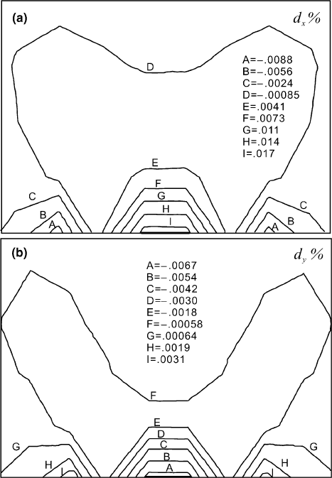
elastically distorted to some extent. The calculated angular distribution of the elastic
distortion above the stretched line segment is shown in Fig. 12.12. Figure 12.12a and
b show the calculated elastic distortion d
x
and d
y
around the line segment with 3%
Fig. 12.12 Calculated elastic distortion d
x
and d
y
around the QWR. (a) d
x
, distortion in the x-
direction; (b) d
y
, distortion in the y-direction. The thick short lines represent the QWR
304 W. Lei et al.
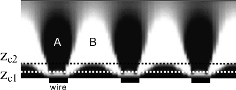
Fig. 12.13 Distribution of the strain component
ε
xx
in a two-dimensional (2D) QWR array calcu-
lated with w = d/4 in isotropic medium, where w and d are the width and lateral period of the
QWRs, respectively. The dark denotes compressive region while the white denotes tensile region.
The rectangles represent the 2D QWRs schematically
elastic extension in the matrix. The figures show that the maximum elastic distortion
is not directly above the wire but staggers away, and the strain angular distribution is
skew away from the wire’s top. Although the calculation is performed for the matrix
with infinite dimension, the results may be appropriate to the practical situation if the
influences of the boundary and the interaction between the extended segments are
not significant. During the epitaxial growth of strained InAs film on InAlAs spacer
layer, QWRs will nucleate and grow in the region where the values of the compo-
nents of the elastic strain field are maximum. As calculated, the strain maximum
in each InAs layer is staggeringly arranged and, as experimentally observed, the
InAs QWRs are indeed diagonally arranged in the multilayer structure [18, 29–31].
Therefore, the calculation is consistent with the experimental observation.
The strain distribution around an embedded quantum wire was also calculated
using the Airy stress function, and Fig. 12.13 shows the calculated distribution of
strain components
ε
xx
around InAs QWRs, where x is the direction along the ar-
ray of QWRs [32, 33]. It can be seen from the figure that with the increase in the
distance away from the QWR array, the material in the region A is first laterally
stretched (
ε
xx
> 0) and then becomes laterally compressed (
ε
xx
< 0). There exists
a critical value z
c1
at which the strain
ε
xx
changes from tensile to compressive. In
contrast, the material in the region B is first laterally compressed and then becomes
laterally stretched. Another critical value z
c2
can be defined in this region. The cal-
culated strain distribution implies that when it is buried deeply enough, the 2D QWR
array will produce compressive surface regions right above the QWRs and stretched
surface regions above the interstices between QWRs, resulting in the vertical anti-
correlation of QWRs in a multiple layer structure.
12.3.2 Effect of Growth Mode on the Symmetry of Wire
Arrangement
As for the growth of self-assembled InAs QWRs on InP substrate, the deposition of
InAs layers can be performed in both conventional MBE and Migration enhanced
epitaxy (MEE) growth modes. The distinction between these two epitaxial modes
