Wang Zh.M. One-Dimensional Nanostructures
Подождите немного. Документ загружается.

11 One-Dimensional Phase-Change Nanomaterials 275
of thermal properties as functions of material size, especially at nanoscale and
low-dimensionality, have not been explored.
Taking chemically synthesized one-dimensional chalcogenide nanowire as an ex-
ample, it can be shown that phase-change materials at nanoscale exhibit exceptional
thermal behavior that may potentially facilitate the effort to surmount the intimidat-
ing memory scaling barrier. We begin with a brief discussion of the pros and cons
of the “bottom-up” and “top-down” approaches to nanotechnology for memory ap-
plications in Sect. 11.2, followed by chemical synthesis, material characterization,
and thermal property study of phase-change nanowire materials of common inter-
est, such as GeTe and In
2
Se
3
, in Sect. 11.3. A summary and future prospects will be
given in Sect. 11.4.
11.2 Top-Down vs. Bottom-Up Approaches in Nanotechnology
In principle, there are two strategies for the implementation of nanotechnology or
nanofabrication: the bottom-up and the top-down. The bottom-up approach attempts
to build nanodevices via chemical synthesis and self-assembly of nanoscale atomic
or molecular components. The top-down approach seeks to fabricate nanodevices
using precision tools such as photolithography (e.g., electron-beam, extreme ultra-
violet, and X-ray). While the latter has been the choice in semiconductor industry
for making microelectronic chips for decades, the core concept of the bottom-up
nanofabrication is to employ inexpensive chemistry to assemble the basic building
blocks. It contains the following processes: synthesis of nanomaterials, implemen-
tation of nanodevice components, and organization/assembly of complex nano-
systems.
The pros and cons of the bottom-up and the top-down approaches are mat-
ters of debate in the literature. The advancement of top-down semiconductor chip
technology has been slowing down owing to increasingly challenging fabrication
limitations such as those associated with the resolution capability of the photolitho-
graphic tools. In the bottom-up approach, fabrication at both material and device
levels are not yet well defined or fully developed. In addition, the connection to
the macro world remains an unresolved problem. While each approach has its ad-
vantages and disadvantages, future nanotechnology implementations might embrace
contributions from both. For example, nanodevices could be made via the bottom-
up strategy and assembled in situ (or “grown in place”) on a nanochip fabricated
via the top-down lithographical techniques with interface to the macro world. This
hybrid nanotechnology allows integration of the advantageous attributes of both ap-
proaches. It is an effective way to investigate the behavior, performance, reliability,
and scalability of nanodevices with ultrasmall critical features implemented alterna-
tively by a quick, feasible, and low-cost process, well before the photolithography
tool offers competitive patterning capability. In such a sense, nanomaterials made
by bottom-up chemical synthesis offer an excellent material platform for advanced
scientific research.
276 X. Sun et al.
11.3 Synthesis and Characterization of Phase-Change Nanowires
(PCNWs)
11.3.1 General Synthesis Techniques
One-dimensional inorganic nanowires are potential nanoscale building components
in future electronic chip applications. Anisotropic crystal growth (whisker) was
found in the ores in 1500s. Laboratory-synthesized 1-D “microwires” (diameter
>1 µm) were first reported as early as in 1960s by Wagner and Ellis [25]. 1-D
“nanowires” (diameter <100 nm) were made possible in the 1990s [26] because of
rapid advancement of both nanoscale fabrication and material characterization tech-
niques. For the synthesis of nanowires, it is necessary to restrict the growth of mate-
rial along the axial direction. A widely used technique is the so-called VLS (vapor–
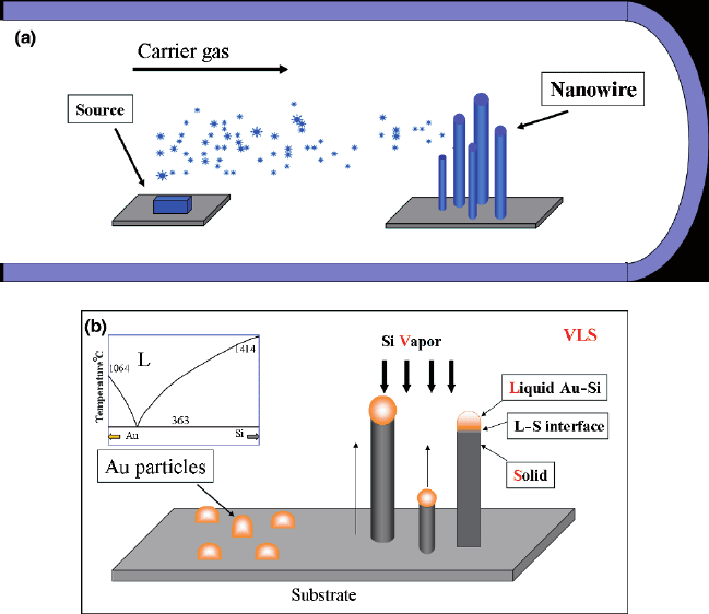
liquid–solid) growth [25]. A schematic diagram of VLS growth via thermal evapo-
ration is shown in Fig.11.1. Here, a solid–liquid interface is introduced through a
Fig. 11.1 A schematic diagram of thermal-evaporation VLS nanowire growth. (a) Thermal evap-
oration and nanowire growth process. (b) Vapor–Liquid–Solid (VLS) mechanism of Si nanowire
growth using Au nanoparticles as the catalyst. Inset: the phase diagram of Au–Si alloy

11 One-Dimensional Phase-Change Nanomaterials 277
metallic nanoparticle serving as catalyst, and the growth occurs only at the solid–
liquid interface, promoting directed growth. The material from a gaseous source
is “dissolved” in the liquid phase of the metal catalyst in the form of a composite
nanoparticle, forming a eutectic mixture. Oversaturated material subsequently crys-
tallizes at the liquid–solid interface, resulting in one-dimensional growth in a con-
tinuous manner. Since this method involves three phases, the vapor phase of the
material source, the liquid phase of the eutectic mixture droplet, and the solid phase
of the nanowire, it is commonly referred to as the VLS growth. This method has
been widely used to grow various types of nanowire [16,27].
In the VLS method, one-dimensional growth is induced and directed by the liquid
droplets of the catalyst metal, whose sizes remain essentially unchanged during the
entire growth process. Hence, each liquid droplet serves as a virtual template to
restrict the lateral growth of an individual wire. Metal nanoparticles of Au, Fe, Ti,
In, etc., have been employed as the metal catalysts in nanowire growth [28–32].
Gold is commonly used in nanowire growth because of its inertness and its ability
in forming a eutectic with many materials at relatively low temperatures. As many
as fifteen metals including gold have been tested for the effectiveness as catalyst in
SnO and silicon nanowire growth, which showed an inverse relation between the
growth density and melting point of the metal [28]. It should be emphasized that,
though often referred to as “catalysts,” the metal nanoparticles play more of the role
as “initiator” and “director” in the form of a “soft template” for the one-dimensional
growth of the nanowires. The advantage of the VLS method is that the diameter of
the nanowire can be controlled by the size of catalytic nanoparticles.
Using the thermal evaporation process and gold (Au)-catalyzed VLS growth, re-
producible synthesis of high-yield, size-controllable, single crystalline chalcogenide
phase-change nanowires on semiconducting (silicon) or insulating (SiO
2
) substrates
has been demonstrated. The diameter control of the NW was achieved by distinc-
tively selecting the size of Au nanoparticles catalyst or the thickness of Au thin
film. The length of NW, depending on the growth time, may extend up to tens of
micrometers. The synthesis of nanowires was carried out in a vacuum two-zone fur-
nace synthesis system. A schematic diagram of the system is shown in Fig. 11.2.
Fig. 11.2 A schematic diagram of a vacuum two-zone nanowire synthesis system
278 X. Sun et al.
In the setup, the nanowire growth temperature (low) and the source evaporation
temperature (high) were separately controlled. The high-purity chalgenide source
powders was placed in the high-temperature zone. The silicon or SiO
2
-coated sili-
con substrate, dispersed with gold nanoparticles as catalyst, was loaded downstream
in the low-temperature zone as target substrate for NW growth. The reactor tube was
evacuated to a base pressure of 10
−2
Torr prior to the growth experiment. Argon was
introduced into the system as a carrier gas during the growth process.
The physical morphology and crystallinity of the as-synthesized NWs was
examined by scanning electron microscopy (SEM, Hitachi S-4000 FEG), high-
resolution transmission electron microscopy (HR-TEM, Philips CM20, operated
at 200 kV) equipped with energy dispersive X-ray spectroscopy (EDX) for chem-
ical composition analysis and selected area electron diffraction (SAED). X-ray
photoelectron spectroscopy (XPS) measurement was performed in an SSI S-Probe
Monochromatized Spectrometer using Al (ka) radiation (1486 eV) as a probe. The
as-grown nanowires were dispersed onto the copper TEM grids (coated with SiO
x
or carbon film) for TEM imaging.
11.3.2 Synthesis and Characterization of IV–VI Compound (GeTe)
Nanowires
A typical synthesis condition for GeTe nanowires is described as follows. High-
purity GeTe powder (99.999%, Aldrich) was placed in the middle of the high-
temperature zone. Gold nanoparticles (20 nm) were dispersed as catalyst on thermal
SiO
2
coated Si(100) substrate. Argon mixed with hydrogen (20%) as carrier gas
was introduced at a flow rate of 25 sccm (standard cubic centimeters per minute)
and at a pressure of 200 Torr. The source furnace temperature was maintained at
680 ∼ 720
◦
C for 1 h and the temperature in the downstream growth zone was
∼450
◦
C.
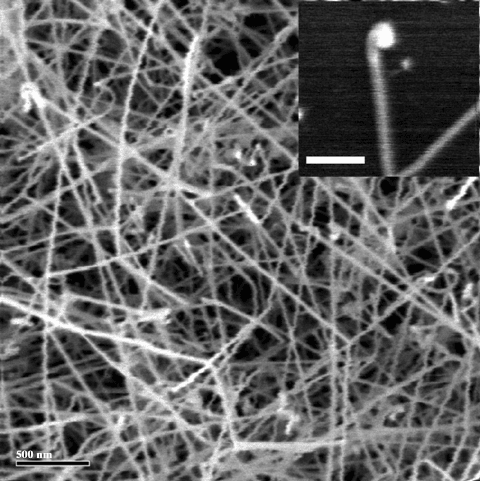
Figure 11.3 shows a SEM image of the as-synthesized GeTe nanowires show-
ing high-yield nanowire growth. Their diameter is in the range of 40 ∼ 80nm and
length up to tens of micrometers. Gold catalyst beads are visible at the tips of
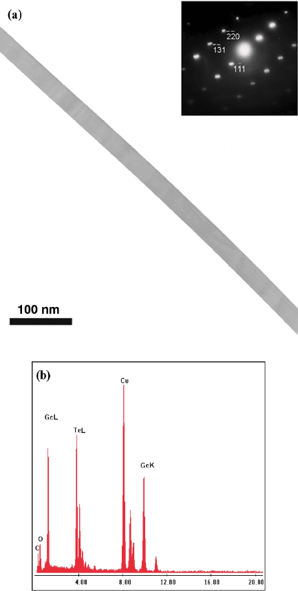
the nanowires, indicating a VLS growth mechanism. Figure 11.4a shows a low-
magnification TEM image of a single GeTe nanowire with uniform diameter of
about 40nm along its entire length. Selected Area Electron Diffraction (SAED) pat-
tern taken from the nanowire (shown in the inset) reveals that the nanowire is a sin-
gle crystal with cubic lattice structure. The EDS analysis of an individual nanowire
confirms that the nanowire (shown in Fig. 11.4b) is composed of only germanium
and tellurium with an atomic ratio close to 1:1. The trace O peak is from the oxide
outer layer, which will be discussed later.
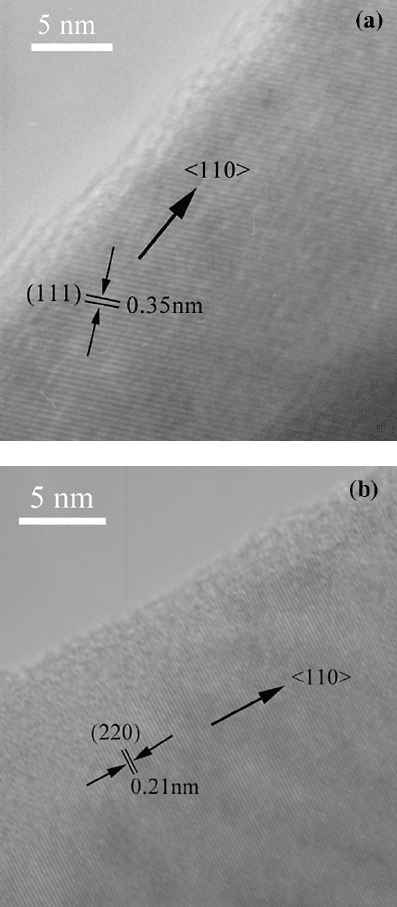
The high-resolution TEM (HR-TEM) image analysis indicates that the as-
prepared GeTe nanowires are high-quality single crystals. Figure 11.5a and b show
that the GeTe nanowire is structurally uniform and contains no noticeable defects
such as dislocations and stacking faults. A layer of 1–3nm amorphous oxide shell
11 One-Dimensional Phase-Change Nanomaterials 279
Fig. 11.3 SEM image of as-synthesized GeTe nanowires on SiO
2
-coated Si(100) substrate using
20 nm Au nanoparticles as growth catalyst. Scale bar is 1µm. Inset: a close-up view of a catalyst
bead at the tip of the single GeTe nanowire. Scale bar (inset) is 200 nm
coverings the GeTe nanowire surface and exhibits an atomically sharp interface.
It is known that the surface of GeTe is oxidized spontaneously in the presence of
atmospheric air to form GeO
2
·TeO
2
[33–35]. The lattice spacing of ∼3.5
˚
Ain
Fig. 11.5a and ∼2.1
˚
A in Fig. 11.5b corresponds to the d-spacing of the (111) and
(220) crystal planes, respectively, of GeTe with a cubic lattice structure. HR-TEM
imaging results and SAED pattern suggest that the GeTe nanowire is single crys-
tal of the cubic structure with lattice constant a of ∼6.01
˚
A, which is consistent
with the JCPDS PDF 03-065-0415 (cubic structure, Fm3m, a = 6.02
˚
A). The GeTe
nanowires have a preferential growth direction in the <110> crystalline orientation.
At room temperature, the GeTe crystal has rhombohedral structure (R3m), which
is transformed to cubic structure (NaCl structure) at high temperatures (∼446
◦
C)
[36]. The rhombohedral structure can be viewed as a distorted NaCl-type structure.
The degree of the distortion from the cubic NaC1-type structure is reflected in the
angle
α
= 88.35
◦
between the axes of the face-centered rhombohedral unit cell,
which differs slightly from the undistorted value of 90
◦
. With increasing temperature
the angle
α
increases from the room-temperature value of 88.35
◦
continuously to
the undistorted value of 90
◦
at about 446.5
◦
C. The growth temperature of GeTe
nanowires is above the transition temperature of GeTe crystal from rhombohedral to
cubic structure. Therefore, the nanowires grown at high temperature exhibit cubic
structures.
280 X. Sun et al.
Fig. 11.4 Morphology and composition of germanium telluride nanowire. (a) Low-magnification
TEM image of an individual GeTe nanowire with a diameter of about 40 nm. The nanowire length
is over 5 µm. Inset: the SAED pattern of an fcc cubic lattice structure. (b) EDS spectrum of the
same GeTe nanowire as shown in panel (a)
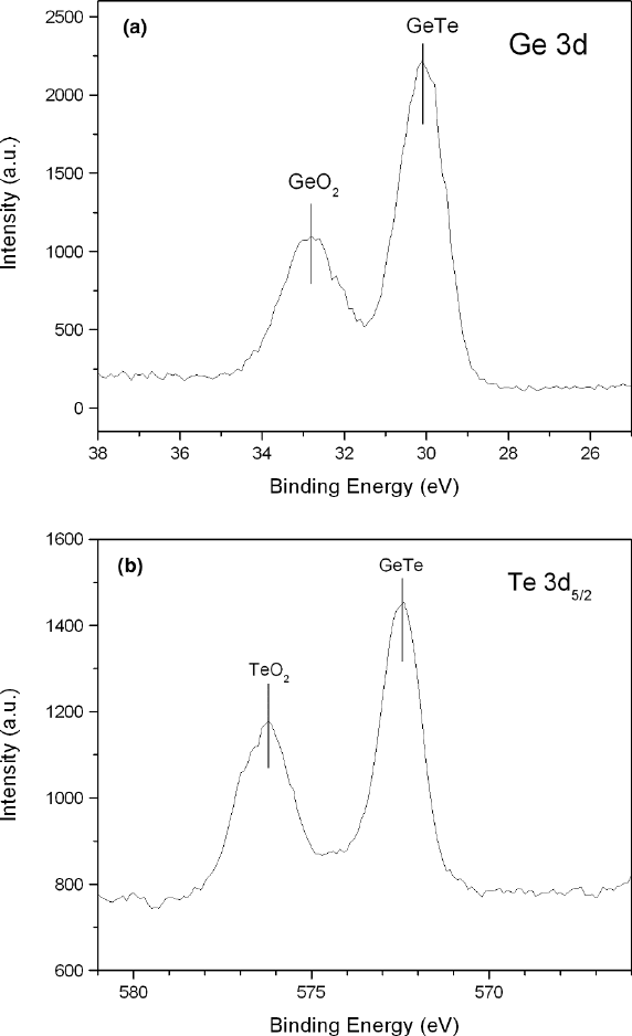
The electronic and chemical state of GeTe nanowires were studied by XPS.
Figure 11.6a and b shows the XPS spectra of Ge 3d and Te 3d
5/2
, respectively. The
binding energies at 30.0 eV in Fig. 11.4a and 572.4 eV in Fig. 11.4b are attributed
to Ge 3d and Te 3d
5/2
in GeTe, respectively, which is in agreement with values
11 One-Dimensional Phase-Change Nanomaterials 281
Fig. 11.5 High-resolution TEM images of the crystal structure of germanium telluride nanowires.
(a) one sample showing (111) planes with an interplane spacing of ∼0.35nm. (b) Another sample
of GeTe nanowire shows (220) planes with an interplane spacing of ∼0.21nm. Both nanowire
samples show an elongation along the preferential <110> crystalline orientation. A thin (1–3 nm)
amorphous oxide layer is observed on the surface in both samples
282 X. Sun et al.
Fig. 11.6 XPS spectra of germanium telluride nanowires with peak representing (a)Ge3dand
(b)Te3d
5/2
. The binding energy information indicates the existence of GeO
2
and TeO
2
in each
case, respectively
11 One-Dimensional Phase-Change Nanomaterials 283
reported in the literature [35,37–39]. The XPS analysis indicates that the nanowires
are GeTe compound. The peaks at 32.8 eV in Fig. 11.6a and 576.2 eV in Fig. 11.6b
are due to GeO
2
and TeO
2
, respectively, from the thin oxide outer layer. Because
XPS is a surface sensitive tool with a sampling depth of several nanometers, even 1–
3nmGeO
2
·TeO
2
outer layer can be clearly detected. A quantitative analysis from
XPS data further confirms that the atomic ratio of Ge and Te is close to 1:1.
11.3.3 Synthesis and Characterization of III–VI Compound
(In
2
Se
3
) Nanowires
The compound semiconductor Indium Selenide (In
2
Se
3
) is of interest due to its
polymorphism and the related metal-ion defect structure. It exhibits at least three dif-
ferent crystalline modifications denoted by α, β, and γ with a transition temperature
of 200 and 650
◦
C, respectively, for the α–β and β–γ transition [40]. Undoped In
2
Se
3
is an n-type semiconductor in the form of hexagonal structure with a direct band gap
of 1.7 eV [41]. In
2
Se
3
is considered for several applications such as photovoltaic so-
lar cell [42, 43], optoelectronics [44], and ionic battery [45]. In particular, In
2
Se
3
has been recently used as a programmable material in phase-change random access
memory (PRAM) [46, 47]. In
2
Se
3
shows four orders of magnitude higher electri-
cal resistivity than Ge
2
Sb
2
Te
5
, a widely used phase-change material for PRAM.
Its resistivity can be varied by a factor of 10
5
, depending on the degree of crystal-
lization. Highly resistive phase-change materials help to reduce the programming
current in PRAM switching activity, especially in the crystal to amorphous (c-to-α)
phase transition. The reduced current implies low energy consumption, minimized
intercell thermal interference, and improved cell scalability in data storage.
A typical synthesis condition for In
2
Se
3
nanowires is described as follows.
In
2
Se
3
powder (99.999%, Aldrich) was placed upstream in the reactor in the middle
of the high-temperature zone. Both Si(111) wafer and 300
˚
A thermal SiO
2
coated
Si(100) wafer, deposited with gold nanoparticles or indium film, were loaded down-
stream in the low temperature zone as the target substrate for nanowire growth.
Argon as the carrier gas was introduced at a flow rate of 25 sccm and pressure of
30∼600Torr, or at a flow rate of 100 sccm and at atmospheric pressure. The tem-
peratures of the source material and that of the targeted substrate were ramped up to
900–950
◦
C and 650–700
◦
C, respectively, and maintained for 60 min.
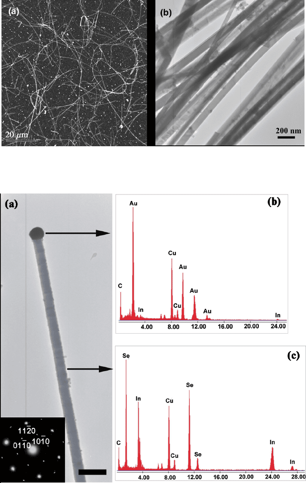
The as-grown In
2
Se
3
NWs have a diameter in the range of 40–80 nm and are up to
100µm in length as shown in Fig. 11.7. A representative TEM image (Fig. 11.8a) of
an individual In
2
Se
3
NW shows that the nanowire has a smooth surface and uniform
thickness along the growth direction. The average diameter of the NWs is 60 ±
18nm. Local EDS analyses (Fig. 11.8b), in which the TEM electron beam is focused
on a targeted sample areas as small as 9 nm in diameter, shows that the particle,
appeared as a dark-colored ball on the tip of the nanowire, is primarily gold with
an indium content below 5 at.% and selenium content below the detection level.
The local point EDS analysis on the nanowire (Fig. 11.8c) shows that In and Se
284 X. Sun et al.
Fig. 11.7 (a) SEM image of the as-synthesized In
2
Se
3
nanowires on SiO
2
-coated Si(100) sub-
strate using 20 nm Au nanoparticles as growth catalyst. (b) TEM image of as-synthesized In
2
Se
3
nanowires
Fig. 11.8 (a) TEM image of In
2
Se
3
NW grown on SiO
2
substrate using 20 nm gold nanoparticles
as catalyst. A metal bead is observed at the tip of the nanowire. Scale bar is 200 nm. SAED pattern
taken on the same NW is shown in inset. (b) EDS spectrum with locally focused e-beam spot on
the bead part (arrow indicated). 5.0 at.% In: 95.0 at.% Au was detected. (c) EDS spectrum with
locally focused e-beam spot on the nanowire part (arrow indicated)
