Wang Zh.M. One-Dimensional Nanostructures
Подождите немного. Документ загружается.

1 Study of Nanowire Growth Mechanisms: VLS and Si Assisted 9
crystal–substrate interfacial area, the contribution from the crystal–substrate inter-
face is not expected to significantly change the order of magnitude of the effect.
Thus, strictly based on the Gibbs–Thompson effect, one can predict the melting
point depression ∆C to be about 65 for the case of the 25–40-nm nanowire tips.
This suggests that for the 610 and 660
◦
C growths, the tips will be almost fully in
the liquid state at 20% In composition. However, for nanostructures on the order of
60 nm, one can expect a much smaller melting temperature reduction from this the-
ory, which will not shift the liquidus line sufficiently. This means that the nanowire
tips with sizes of 60 nm shown in Table 1.1 will remain in a partially solid state dur-
ing growth and those grown below the eutectic would not exhibit any liquid state at
all. However, several published experimental results reported much larger melting
point suppression in nanostructures [27–29] than predicted by pure theory, and thus
it is useful to consider these. These studies include the vaporization of Au particles
on graphite [27], melting of thin In film on an amorphous silicon nitride membranes
(a−SiN
x
) [28], and melting of Ge nanowires [29]. For the studies on surfaces, the
substrate materials were carefully chosen so that they had a very low affinity to the
nanostructure being studied, since the melting behavior of nanostructures is known
to be strongly influenced by the surrounding environment [30,31].
From the above published works, the melting point reduction results reported
by Wu and Yang [29] on 30-nm diameter Ge nanowires may be of interest, since
similar nanostructure sizes were studied as in our experiments. In the case of the
Ge nanowires, a 25% melting point reduction was reported during heating of
the nanowires in a TEM. This is a much more significant effect than would be
predicted from pure theory. For example, for a similar diameter Ge nanowire, the
Gibbs–Thomson expression for the melting point depression is (T
r
−T
m
)/T
m
≈
γΩ
/rL. Using the values for Ge (
γ
= 1.4Jm
−2
,
Ω
= 13.6cm
3
mol
−1
, L =
36.94kJ mol
−1
) and a radius of 30 nm gives a melting temperature reduction of
only 2%, yet this is an order of magnitude smaller than the experimental value re-
ported. Thus, although Ge is a different material, these experimental results indicate
that far larger melting temperature reductions can occur than would be predicted by
the Gibbs–Thompson effect.
If we now examine our experimental results, it is possible to estimate the extent
of melting point depression, assuming a uniform drop of the liquidus, as suggested
by Vallee et al. [32] (of course in this respect, the correct description would be
termed a liquidus depression, and not melting point depression). For the nanowires
grown at 400
◦
C, we can estimate ∆C, the amount of melting point reduction, to be
about 250, which is about four times that of the value predicted from the Gibbs–
Thompson effect for Au, as calculated above. Although it is true that the calculation
was performed on pure Au and not on Au–In alloy for which no data exist, it is still
clear that the melting point reduction estimated from our experiment far surpasses
what the theory would predict. This is a similar magnitude as the large melting point
reduction reported in the case of the 30 nm Ge wires, in which the Gibbs–Thompson
theory only predicts a 2% drop. The reason for this large size-dependent melting
reduction is not clear at this point, but these results suggest that additional factors
must be considered in the theory in the case where the sizes are at or below 60 nm.
10 H.D. Park, S.M. Prokes
Taking into account the size-dependent liquidus depression factor in a binary
system, the results of Kamins et al. [24] and Persson et al. [11] (as well as those of
Dick et al. [12]) should be revisited and reinterpreted. In the case of Ti-catalyzed
Si nanowires reported by Kamins et al., the nanowire growth temperature is so be-
low the Ti–Si eutectic temperature that the liquidus depression factor does not seem
applicable at all in this particular case. It is very unclear what process may be occur-
ring, but it appears to be the only nanowire growth with a solid metal alloy tip during
the nanowire growth. For the Persson et al. (and Dick et al.) results in the derivation
of VSS growth mechanism, however, the liquidus depression factor seems to con-
tradict the claim of a solid metal alloy tip. The authors reported a low Ga(In) content
in the Au–Ga(Au–In) binary system required for the eutectic melt measured at the
nanowire growth temperature near the Au–Ga eutectic (Au–In), but if the liquidus
depression factor is taken into consideration, the Au–Ga(Au–In) was most likely in
liquid state, and not solid, during the nanowire growth. This result then implies that
the nanowires grew according to the VLS and not VSS growth mechanism.
One further consideration needs to be emphasized: The Au nanoparticles resting
on an InAs substrate (forming Au–In alloy) present quite a reactive system, a fact
which was not considered by Persson et al. (and Dick et al.). Earlier in the derivation
of the VSS growth mechanism, Persson et al. stated that the size-dependent melting
point depression factor was not considered due to the larger size of the Au–Ga alloy
seed particle (20–70 nm) examined in their growth, compared with the size of the Au
nanoparticle (2–5 nm) examined in the work of Buffat et al. (a work which they had
referenced), where the size-dependent melting point depression was observed [27].
It is important, however, to point out that many of the previous size-dependent melt-
ing point depression studies were done on the substrate materials that had a very low
affinity to the nanostructure being studied, since the melting behavior of nanostruc-
tures is known to be strongly influenced by the surrounding environment [30,31]. In
the work of Buffat et al., for example, the size-dependent melting point depression
of Au nanoparticles has been examined on an amorphous carbon surface which has
a minimal interaction with Au. This description of minimal nanostructure–substrate
surface interaction cannot be applied for a system of Au on the GaAs and InAs
substrates, where Au forms an intermetallic phase even at low temperature with Ga
and In.
Although there seems to be differing (and contradictory) results with the newly
proposed VSS growth mechanism, one thing that should be mentioned is that the
growth systems (MOCVD, MBE, etc.) are all different, and thus more research is
needed to clarify the VLS and VSS growth mechanisms with the decrease in the
dimension of the metal alloy particles.
1.3 Si-Assisted Growth Mechanism
To investigate the effect of SiO
x
on the growth of InAs nanowires, we performed
growths [21] on two types of substrates, InAs(111)B and Si(111), with 1.3 nm
of SiO
x
(no Au catalyst). We first examined the growth in the absence of any
1 Study of Nanowire Growth Mechanisms: VLS and Si Assisted 11
400 nm
400 nm
300 nm
200 nm
200 nm
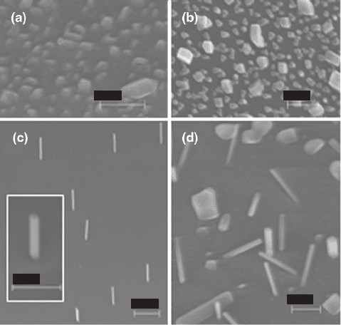
Fig. 1.5 InAs deposits on (a) InAs(111)B (scale bar 300 nm) and (b) Si(111) (scale bar 200 nm)
substrates without any SiO
x
and native oxides. InAs nanowires on (c) InAs(111)B (scale bar
400 nm) and (d) Si(111) (scale bar 200 nm) substrates with 1.3 nm of SiO
x
. Insert in (c)isthe
close view of the InAs nanowire (reprinted with permission from [21], Copyright 2006, American
Institute of Physics)
SiO
x
(including native oxides), and the results of growth on bare InAs(111)B and
Si(111) substrates are shown in Fig. 1.5a and b, respectively. The images show var-
iously shaped InAs islands, with the structures on the Si(111) substrate revealing
more crystalline features. We next used 1.3 nm of SiO
x
and the growth results on
InAs(111)B and Si(111) substrates are shown in Fig. 1.5c and d, respectively. Inter-
estingly, the typical diameter of the nanowires was about 20–30 nm on both sub-
strates, and the resulting lengths were quite similar. However, while the growth
direction of the nanowires on the InAs(111)B was along the 111 direction, the
growth direction on the Si(111) was random, as shown in Fig. 1.5d. In Fig. 1.6a
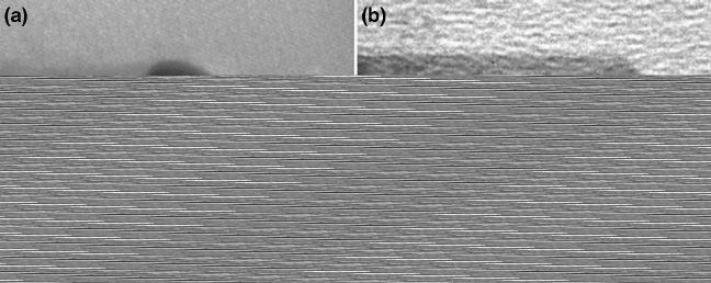
and b, the TEM images of the VLS and SiO
x
-grown InAs nanowires are shown,
respectively, at the point of their growth termination. As can be seen, the terminat-
ing surface of the SiO
x
-grown nanowire is flat and absent of any catalyst particle,
unlike the typical VLS- (and VSS)-grown nanowires. Inset in Fig. 1.6b shows the
opposite end of the nanowire (typically fractured), identifying it as the base of the
nanowires where it had broken off from the substrate during TEM sample prepa-
ration. The electron diffraction pattern also revealed SiO
x
-grown nanowires to be
single crystal.
Growth was also attempted with only the native oxides of InAs (In–O
x
and
As–O
x
), where no Au catalyst was used. The HCl-etched InAs substrate was left
12 H.D. Park, S.M. Prokes
Fig. 1.6 Growth terminating points for the (a)VLSand(b) Si-assisted grown nanowires. Insert
shows the wire end broken off the substrate (reprinted with permission from [21], Copyright 2006,
American Institute of Physics)
out in the air and allowed to oxidize at room temperature for 3 days prior to growth
(no Au catalyst was used). The expected native oxide thickness for an HCl-etched
InAs substrate, oxidized at room temperature for 3 days, will be approximately
10
˚
A [33]. After a growth time 30 min in the furnace, the substrate was examined
under SEM, but unlike in the SiO
x
case, no growth was noted in this case.
Finally, to examine the VLS and the SiO
x
growth simultaneously, Au nanopar-
ticles were deposited on existing 1.3-nm SiO
x
on the InAs(111)B substrate. In this
case, catalyst-free nanowires still grew (as evidenced by the uniform 20-nm
diameters and random growth directions), but no Au-mediated nanowires were
noted in the 30 min growths. However, some were found to grow after longer
growth times.
Now, let us consider the effect of an oxide layer on the growth of these nanowires.
As discussed earlier, no nanowire growth occurred when the substrate contained a
thin In- or As-based suboxide. This would suggest the deleterious nature of oxy-
gen on the resultant nanowire growth. However, the results were quite different
when a silicon suboxide layer was present, where InAs nanowires of characteristic
20–30 nm diameters grew. This suggests that the type of oxide, and not the presence
of oxygen alone, may be the determining factor.
In the case of a silicon suboxide, the stoichiometry of evaporated SiO
x
films is
strongly dependent on various evaporation parameters, such as temperature, pres-
sure, and rate of evaporation [34]. Since our deposition conditions were very similar
to those used in the previous study [35], we expect x ≈ 1 for our SiO
x
film. It is well
known that SiO undergoes a phase separation reaction (2SiO → Si + SiO
2
) [34]
at higher temperatures (T > 400
◦
C), yielding nanometer-sized Si clusters [36, 37].
We would thus expect this phase separation to occur at our growth temperature of
580
◦
C. Since Zhang et al. [38] have reported that Si clusters in the silicon suboxide
are energetically very reactive, while SiO
2
is quite stable, one would expect that
these nanometer-sized Si clusters could enhance the In attachment rate at the clus-
ter surface sites. Since the silicon clusters are in solid state at 580
◦
C, the growth
166 T. Laroche, A. Vial
FDTD
Fit
R=0.21
L=3.16 µm
∆I/I
min
I
min
λ(nm)
I
output
/I
input
∆Ι
l=4 mm
0.4
0.2
700 900
0.6
0.1
0.2
0.3
0.4
2 4 6 8 10 12 14
Nanowire’s length (µm)
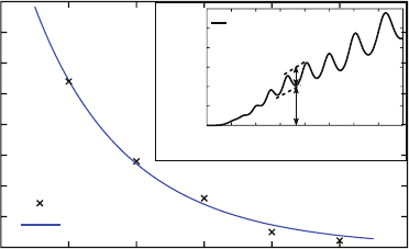
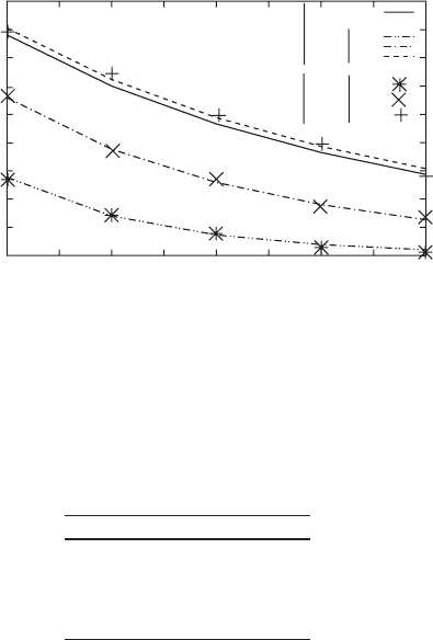
Fig. 7.11 Spectral relative modulation depth (∆I/I
min
) at a wavelength equal to 785nm versus
nanowire length. The crosses give the theoretical values obtained by FDTD computation for five
different lengths of nanowire with diameter equal to 120 nm. The solid line is the fit of the Fabry–
Perot cavity model. The inset (normalized transmittance spectra computed for 4 µm long nanowire)
shows the measure of ∆I and I
min
Although the numerical propagation length (computed here with Palik’s silver data)
is three times weaker than the experimental value measured in [28], our results con-
firm that silver nanowires behave as efficient optical resonators.
7.3.4 Conclusion
In this part, we have simulated the electromagnetic field transfer along a metallic
nanowire deposited on a dielectric substrate. Our FDTD study confirm the exper-
imental results about the similarity between metallic nanowires and Fabry–Perot
cavities. We have also compared the behavior of such a nanostructure with a discon-
tinuous one. Unlike what happens with chains of nanoparticles which open a narrow
band [31], the spectra of nanowires reveal the longitudinal mode structure. As ex-
pected, by using the bulk permittivity of silver, we have found an effective surface
plasmon wavelength and a propagation length of the surface plasmon mode which
differ from the experimental ones for a single silver nanowire. In fact, by intro-
ducing bulk dielectric data in our FDTD code, the metal is treated as an amorphous
medium so they do not completely match the monocrystalline features of silver wire
used in [28]. Since the dielectric constant in visible range of such photonic elements
is not well known in the literature, the numerical scheme described in this part could
be used to fit parameters able to provide the permittivity of monocrystalline metallic
nanostructures. For example, this might be realized by varying the mean free path of
the electrons in the Drude–Lorentz model (through γ
D
,
Γ
L
) used in this study. This
is the topic of our next section.

7 FDTD Spectroscopic Study of Metallic Nanostructures 167
7.4 Further Improvements of the Dispersion Models
in Order to Take into Account the Fabrication Process
of the Nanoscale Structures
The usual tabulated data of the permittivity [27, 32–34] are defined for bulk thin
layer but always for amorphous materials. Although this values are commonly em-
ployed in most of the simulations about optical dispersive phenomena in nanostruc-
tures, they should not be used for all cases. Indeed, we have seen in Sect. 7.3 that
they do not lead to the experimental value of propagation length of the surface plas-
mon for a single monocrystalline silver nanowire. So, we have to take into account
the fabrication process in the nano-optic simulation. In fact, each process provide a
peculiar crystalline structure, which leads to a specific optical dispersive behavior.
In this part, we demonstrate a efficient mean to obtain theoretical results in better
agreement with experimental ones for a monocrystalline nanostructure. Further, this
method enables us to determine the real permittivity of the nano-structured material.
7.4.1 A Mean to Adapt the Tabulated Permittivities to a Specific
Nanostructure
A large part of the nano-optic community agrees that the permittivity of nano-
structured objects dissent from the bulk values. In metallic nanostructures, the mean
free path of the electrons is modified when the size of the structure decreases. This
phenomena should increase the damping inside the nanostructure and thus change
the permittivity [35].
In our case, the silver nanowire depicted in Fig. 7.5 is a monocrystalline nanos-
tructure. So, the previous argument does not work here. Indeed, the mean free path
increases because of the absence of the crystalline domains walls. However, the ap-
proach is fairly similar to the one used for the damping phenomena [35]. Instead
of modify the damping of the Drude and Lorentz models to decrease the mean free
path of the electrons, we increase it.
To achieve this for the silver nanowire, we multiply the previous Drude–Lorentz
constants γ
D
ans γ
L
in Table 7.1 by a constant
κ
and Eq. 7.73 becomes
DL
(ω)=
∞
−
ω
2
D
ω(ω + i
κ
γ
D
)
−
∆
Ω
2
L
(ω
2
−
Ω
2
L
)+i
κΓ
L
ω
. (7.77)
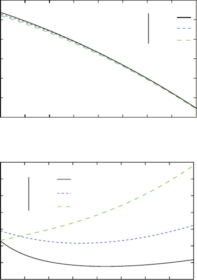
In order to verify that only the imaginary part of the permittivity is significantly
modified, we plot the real and imaginary parts of the permittivity against the excita-
tion wavelength for three values of
κ
(see Fig. 7.12).
In Fig. 7.12a, the real part of the silver’s permittivity is fairly the same whatever
be the
κ
coefficient. On the contrary, we show in Fig. 7.12b that the mean of the
imaginary part decrease with the value of
κ
all along the wavelength range.
168 T. Laroche, A. Vial
λ(nm)
Re (ε)
λ(nm)
Im (ε)
(a)
(b)
κ
κ
1
400 500 600 700 800
0.4
0.6
0.8
1.2
1.4
1.6
−25
−20
−15
−10
−5
500 600 700 800400
0
=0.25
=0.5
=1
=0.25
=0.5
=1
Fig. 7.12 Fit of the silver’s permittivity. The mean free path correction is taken into account with
the parameter
κ
. There is no correction when
κ
= 1. (a) Fit of the real part of the permittivity ans
(b) for the imaginary one
However, even if this method allows us to theoretically control the mean free
path of the electron in silver, we are not yet able to find the value of
κ
, which match
the permittivity of single monocrystalline silver nanowire. To this end, we have to
employ an empiric method. Otherwise said, we try to match experimental results by
varying the
κ
coefficient in our numerical computation.
7.4.2 Influence of the Mean Free Path on the Guiding Efficiency
for a Single Silver Nanowire
Once again, we numerically study the transmittance spectra of the single silver
nanowire depicted in Fig. 7.5 but we now care about the influence of the mean
free path of the electrons on the surface plasmon guiding efficiency. Indeed, we
7 FDTD Spectroscopic Study of Metallic Nanostructures 169
demonstrated that the theoretical and experimental propagation lengths differ when
the tabulated permittivity are used to simulate the dispersive aspect of silver (see
Sect. 7.3.3). Here, we increase the mean free path to take into account the monocrys-
talline behavior of the nanowire. For each values of
κ
(
κ
= {0.25, 0.5,1}), we apply
the same procedure as in Sect. 7.3.3 in order to compute the spectral modulation
depth versus the nanowire’s length. We show these results in Fig. 7.13 for a wave-
length equal to 785 nm.
The previous result obtained for
κ
= 1 in Fig. 7.11 is plotted in Fig. 7.13 with
stars for FDTD results and with double dotted dashed line for the Fabry–Perot fit.
We also plot the fit of the experimental results found in [28] with solid line. It may
be seen in Fig. 7.13 that the mean value of the spectral relative modulation depth
increases when the value of
κ
decreases. Moreover, the calculation of the different
fits shows that the reflectivity and the propagation length of the surface plasmon
increase too. In Table 7.2, we summarize the coefficient of the fit for each value of
κ
as well as the experimental results of [28].
It may be seen that the reflectivity and the propagation length are in good agree-
ment with the experimental ones when
κ
= 0.25. This result allows to define a new
∆
I/I
min
Fit
FDTD
κ=
κ=
Nanowire’s length (µm)
0.4
0.6
0.8
experimental
1
0.5
0.25
1
0.25
0.5
4681012
0.2
Fig. 7.13 Spectral relative modulation depth at a wavelength equal to 785 nm versus nanowire
length for several values of the
κ
coefficient. The different crosses give the theoretical values
obtained by FDTD computation for each value of
κ
. The different lines are the fits of the Fabry–
Perot cavity model for each value of
κ
. The solid line is the fit of the experimental values obtained
in [28]
Table 7.2 Reflection coefficient and propagation length of surface plasmon in a single silver
nanowire for several values of
κ
κ
RL(µm)
1 0.21 3.16
0.5 0.213 6.1
0.25 0.217 10.2
Experimental 0.216 10.1
The experimental line of this table summarize the values found in [28]
170 T. Laroche, A. Vial
I
output
/I
input
λ (nm)
l = 10 µm
l = 12 µm
l=6 µm
l=4 µm
l=8 µm
0.1
0.3
0.5
0.7
0.9
600 700 800 900 1000
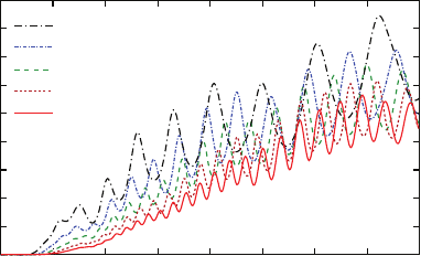
Fig. 7.14 Normalized transmittance spectra computed for five different lengths of silver nanowires.
The configuration is the same as in Fig. 7.6. The dispersive aspect is taken into account with
κ
= 0.25
permittivity for the single monocrystalline silver nanowire, which is given by the
solid line in Fig. 7.12a for the real part and in Fig. 7.12b for the imaginary part.
We have also computed the transmittance spectra for five different lengths of silver
nanowire, results are displayed in Fig. 7.14. For all lengths, the modulation depth is
greater than the one found with
κ
= 1 in Fig. 7.6. Moreover, the mean value of the
transmittance is higher whatever be the length of the nanowire.
7.4.3 Conclusion
In this part, we have adapted the common tabulated permittivity to simulate a
specific experimentation. We demonstrated a numerical method leading to a better
correlation between experimental and theoretical results and we are now able
to describe the propagation of surface plasmons on a monocrystalline metallic
nanowire, in good agreement with experiments.
Our method is still in its early stage of development, as we used the same empir-
ical parameter to modify both the Drude and the Lorentz parts of the permittivity.
In further studies, different parameters could be employed for each term of the per-
mittivity. The optimization of these parameters would require the use of specific
methods like evolutionary algorithms, already successfully applied to the recover-
ing of different kind of nanostructures properties [36].
7 FDTD Spectroscopic Study of Metallic Nanostructures 171
7.5 Concluding Remarks
An FDTD approach has been presented for the study of the dispersive properties of
metallic nanostructures with particular interest in monocrystalline silver nanowires.
In Sect. 7.2, we described several numerical methods to take into account the dis-
persion of the permittivity in FDTD calculations. These methods are mainly based
on the common dispersive models (e.g., Drude or Lorentz model) as well as the
recently introduced critical points model. We also discussed the validity of these
models for silver and aluminium.
In Sect. 7.3, we applied the previous dispersive numerical method (the recursive
convolution method associated to Drude–Lorentz model) to study the dispersive
properties of a silver nanowire. We showed that the physical phenomena yielding
an optical information transfer along metallic nanostructures are drastically differ-
ent in continuous and discontinuous configurations. In fact, this transfer is achieved
by surface plasmon propagation in continuous nanostructures whereas it is the cou-
pling between the surface plasmon on each particle in the discontinuous case. The
silver nanowire can be compared to a Fabry–Perot cavity, and numerical results are
qualitatively in fairly good agreement with the experiment. However, the experi-
mental parameters fitting the behavior of the nanowire significantly dissent from the
numerical ones. Indeed, the simulated experiment takes into account a monocrys-
talline nanowire whereas we use the bulk permittivity commonly tabulated for our
numerical simulations.
In Sect. 7.4, we demonstrated a method to simulate the monocrystalline property
of the nanowire. We showed that we are able to describe this property starting
from the bulk permittivities by modifying the damping in dispersive models. By
decreasing the damping, we obtained numerical results in better agreement with the
experimental ones. This emphasize the fact that the permittivity of a nanostructure
may be different from the corresponding bulk, and the numerical method outlined
in Sect. 7.4 provides a first approach to the estimation of the effective permittivity of
the
nanostructure.
We have highlighted the paramount character of the crystalline property in the
understanding of nanostructures behavior. In several fabrication process, properties
of nanostructures drastically differ from those of the bulk counterparts. Therefore,
we do not afford to simulate all nanostructures by using tabulated permittivity and
we have to take an interest in the crystalline properties of the nanostructures.
References
1. K. Imura, T. Nagahara, and H. Okamoto. Plasmon mode imaging of single gold nanorods.
J. Am. Chem. Soc., 126:12730–12731, 2004.
2. K. Imura, T. Nagahara, and H. Okamoto. Near-field optical imaging of plasmon modes in gold
nanorods. J. Chem. Phys., 122:154701, 2005.
