Ramanathan Sh. (Ed.) Thin Film Metal-Oxides: Fundamentals and Applications in Electronics and Energy
Подождите немного. Документ загружается.

58 D. Ruzmetov and S. Ramanathan
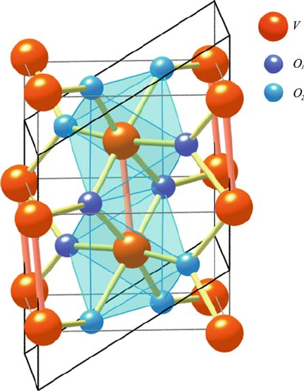
Fig. 2.6 Monoclinic M
1
lattice of the low temperature (below T
SPT
) semiconducting phase of
VO
2
. Two types of oxygen atoms [29, 34] are differentiated. (From Eyert [29] with permission.
Copyright (2002) by Wiley-VCH Verlag GmbH & Co. KGaA)
The structural phase transition involving VO
2
lattice transformation from
tetragonal to monoclinic is generally believed to happen in concomitance with
the metal insulator transition .T
SPT
D T
MIT
/ [6, 35, 36]. However, it has been also
suggested recently that the formation of the tetragonal lattice occurs at a different
temperature than MIT does .T
SPT
¤ T
MIT
/ with the difference being up to 9
ı
C[37].
Thin film VO
2
is often of polycrystalline structure with the grain size in the
range of 30–120nm depending strongly on the film growth conditions [8, 15, 38–
40]. Single crystal thin film VO
2
can be epitaxially grown on sapphire substrates
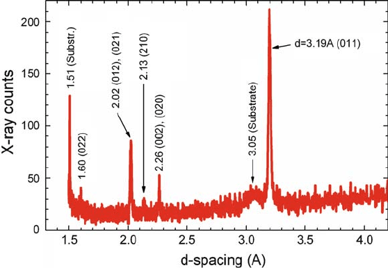
by means of MOCVD [41]. Figure 2.7 shows the XRD spectrum taken using Cu
K’ radiation in ™–2™ geometry from thin film VO
2
on a Si (001) substrate at
room temperature. The thin (100-nm thick) film was reactively DC sputtered in
Ar.91:2%/ CO
2
.8:8%/ environment at 10 mTorr from a V target. The details of the
measurement are given elsewhere [16]. The d-spacings are inscribed in the figure
and the line assignment is done for VO
2
peaks. The XRD spectrum corresponds to
stoichiometric polycrystalline VO
2
in insulating phase.
2 Metal-Insulator Transition in Thin Film Vanadium Dioxide 59
Fig. 2.7 XRD spectrum from a VO
2
thin film on Si.001/=SiO
2
(native oxide) substrate. d values
(in
˚
A) of the peaks are inscribed and for VO
2
lines corresponding Miller indices of the Bragg
planes are given in brackets (From Ruzmetov et al. [16] with permission. Copyright (2008) by the
IOP Publishing Ltd)
2.4 The Relationship between Electron Transport
and Material Morphology
The electrical parameters of the metal insulator transition (MIT) in VO
2
vary
significantly for thin films and bulk crystals, and for thin films prepared at different
conditions [9]. The magnitude of the electrical resistance change at the MIT in thin
films and the temperature width of the transition are generally not as sharp as it is
found in single crystal VO
2
. Although there has been considerable research done on
VO
2
thin films, the mechanisms responsible for the deterioration of the MIT param-
eters – the decrease in R and spread of T
MIT
– in polycrystalline thin films are
not yet well-understood. In this section, we analyze how material synthesis condi-
tions and material morphology affect the electrical parameters of the phase transition
in an attempt to uncover the microscopic mechanisms underlying the macroscopic
observables of the MIT.
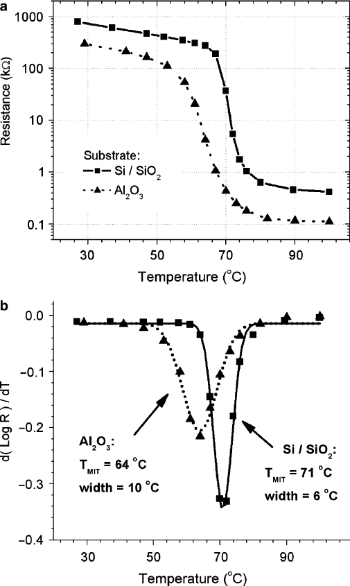
Figure 2.8a shows the temperature dependence of the resistance of 50-nm
thick VO
2
films RF-sputtered from a VO
2
target under identical conditions on
Si=SiO
2
.400 nm/ and r-plane sapphire .Al
2
O
3
/ substrates [24]. These electron
transport measurements demonstrate that the sputtering method described in [24]
allows synthesizing VO
2
films on technologically important Si-based substrates
with the MIT parameters comparable to some of the best reported VO
2
thin films
[9]. In order to precisely determine the transition temperature .T
MIT
/ and its width
we show in Fig. 2.8b the derivative of log
10
R.T / for the data in Fig. 2.8awhich
60 D. Ruzmetov and S. Ramanathan
Fig. 2.8 (a) Resistance versus temperature of 50-nm thick VO
2
films on Si=SiO
2
(400 nm) and
r-plane Al
2
O
3
(sapphire) substrates showing a sharp metal–insulator transition. (b) The derivatives
of Log
10
R.T / for the curves in (a) are shown. Symbols are data points, the lines are Gaussian fits
whose minima and widths determine the T
MIT
and MIT width. (From Ruzmetov et al. [24] with
permission. Copyright (2007) by American Institute of Physics)
are fitted with Gaussians. The centers and widths of the Gaussian peaks are taken
as T
MIT
and MIT widths. Different substrates exert tensile or compressive strain
on a VO
2
lattice causing the shift of T
MIT
[14]. The VO
2
film grown on Si has
2 Metal-Insulator Transition in Thin Film Vanadium Dioxide 61
Fig. 2.9 (a) The normalized resistance of VO
2
films of different thickness: 50 nm and approxi-
mately 7 nm. Sputtering conditions are identical for the two data sets. The substrate is Al
2
O
3
.The
thinner film has considerably sharper MIT. (b) The normalized resistance of two 2-terminal devices
and an unpatterned film. The devices are VO
2
stripes (size d d ,whered D 20 m; 500 m)
contacted with Pt leads. No size dependence is observed for devices scaled down to 20 m. The
increased R value of the 20-m stripe in the metallic state is due to the higher contact resistance.
(From Ruzmetov et al. [24] with permission. Copyright (2007) by American Institute of Physics)
T
MIT
D 71
ı
C, whereas VO
2
on sapphire has T
MIT
D 64
ı
C, which are on different
sides from the published single crystal value T
MIT
D 66
ı
C. Therefore, the substrate
can be used to tune the MIT parameters.
In order to use vanadium dioxide in scaled phase transition devices it is important
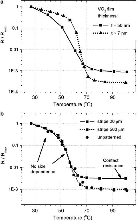
to investigate how the MIT parameters scale with the device size. Figure 2.9ashows
62 D. Ruzmetov and S. Ramanathan
the normalized resistance of VO
2
on sapphire measured at two spots on a sample
with varying film thickness. We see considerable improvement of the MIT parame-
ters when the film thickness is reduced from 50 nm to approximately 7 nm. We can
conclude that under these synthesis conditions the thinner film shows larger resis-
tance drop at MIT and narrower transition width. The reason is discussed further in
the text.
On the other hand the change of the lateral size of a two-terminal VO
2
device
does not produce significant changes in MIT parameters as shown in Fig. 2.9b. In
Fig. 2.9b, three data sets are shown for lithographically patterned VO
2
stripes with
Pt/Ti (adhesion layer of 4 nm) contacts and unpatterned film directly contacted by
electrical probes separated by 3 mm. The stripe sizes between the Pt contacts are
20 m 20 m .50 nm thick/ and 500 m 500 m 50 nm. The increased
value of the resistance in the metallic phase for 20 m stripe is due to higher contact
Pt=Ti=VO
2
resistance of the smaller device (inversely proportional to the lateral
size). The data demonstrate no changes of the MIT upon lateral scaling down to
20-m devices.
It was previously demonstrated that VO
2
films sputtered at higher substrate
temperatures have larger grain sizes and higher crystalline order [39]. Here we in-
vestigate how VO
2
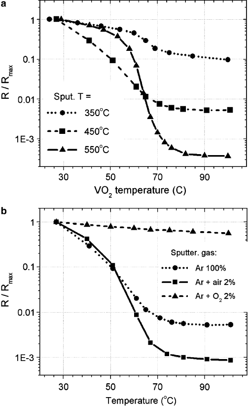
morphology affects MIT parameters. Figure 2.10ashowsMIT
in three samples sputtered at different substrate temperatures. We see that the mag-
nitude of the resistivity drop increases monotonously with increasing sputtering
temperature and consequently the increase in VO
2
grain size and crystalline order.
However, we also observe the non-monotonous behavior in transition width which
may be a result of two competing phenomena affecting the MIT sharpness in oppos-
ing manner with respect to the sputtering temperature: the stabilization of the pure
VO
2
phase and improving of the crystalline order. Higher substrate temperature
during the sputtering was shown by means of electron diffraction measurements to
improve crystalline order of VO
2
[26], which is expected to narrow the MIT width
and enhance the transition since the strongest MIT values were found in VO
2
sin-
gle crystals. On the other hand, higher substrate temperature promotes oxygen loss
which deteriorates the overall VO
2
stoichiometry and results in the larger proportion
of the additional substoichiometric phases of the vanadium oxide, such as V
2
O
3
for
instance. The appearance of such VO
x
phases .x ¤ 2/ makes the MIT due to VO
2
component less pronounced. If this scenario is true then we expect that an addition of
small amount of oxygen in the sputtering gas should compensate for the oxygen loss
and improve (make more pronounced) the transition in samples sputtered at high
temperatures. Figure 2.10b shows the MIT of three VO
2
films sputtered in varying
partial oxygen pressures. Adding 2% of air to the Ar-sputtering gas increases the
resistance drop by an order of magnitude with respect to the films sputtered in pure
Ar. Further increasing of the oxygen partial pressure results in films of higher oxi-
dation states of vanadium so that the MIT almost disappears: see resistance curve in
Fig. 2.10b for the film sputtered in 2% oxygen in addition to Ar.
Figure 2.11 shows thermal hysteresis loops of VO
2
films sputtered on a sapphire
substrate at different conditions. For comparison, representative data from a film
sputtered from a VO
2
target is given along with the data from a VO
2
film reactively
2 Metal-Insulator Transition in Thin Film Vanadium Dioxide 63
Fig. 2.10 (a) The MIT in three VO
2
films sputtered in Ar at different substrate temperatures.
The resistance drop is increasing with increasing sputtering temperature. The MIT width changes
nonmonotonously with sputtering temperature. (b) The MIT of three films sputtered on sapphire
substrate in different gas environments. The substrate temperature during sputtering is 450
ı
C.
(From Ruzmetov et al. [24] with permission. Copyright (2007) by American Institute of Physics)
sputtered from a V target in 84% Ar C 16% air environment. We see qualitatively
different hysteresis shapes for the films sputtered by different methods. The hys-
teresis loop in Fig. 2.11a extends for 34
ı
C with its width not exceeding 4:3
ı
C. The
hysteresis of the reactively sputtered film is squarer and extends for 24
ı
C with width
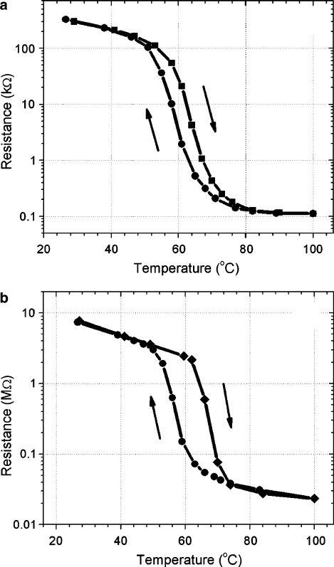
64 D. Ruzmetov and S. Ramanathan
Fig. 2.11 Thermal hysteresis curves of VO
2
thin films on Al
2
O
3
substrate. (a)VO
2
film is
sputtered in pure Ar from a VO
2
target at substrate temperature T
subs
D 550
ı
C. The width of
the hysteresis loop is T D 4:3
ı
C. (b)VO
2
film is reactively sputtered from a V target at
T
subs
D 450
ı
C. The width of the hysteresis loop is T D 10
ı
C. (From Ruzmetov et al. [24]
with permission. Copyright (2007) by American Institute of Physics)
up to 10
ı
C. These differences may reflect different morphologies of the films. As
argued by Lopez et al. [42], the phase transition in VO
2
is nucleated on defects since
the homogeneous nucleation is inhibited due to a high potential barrier originating
from surface free energy increase on a nucleating site. According to the formalism
suggested by Lopez et al., the probability of finding a potent defect in a particle of
2 Metal-Insulator Transition in Thin Film Vanadium Dioxide 65
volume V increases with either V or jT T
MIT
j. Then in smaller particles larger
thermal hysteresis is expected as was confirmed experimentally [42]. We can con-
clude from the data in Fig. 2.11 that the reactively sputtered film in Fig. 2.11bhas
smaller average grain size than the film in Fig. 2.11a, which is reflected in the larger
hysteresis width. These arguments do not explain the difference in the sharpness, or
transition width T
MIT
, in the two graphs. The MIT widths, measured as FWHM of
d.Log
10
R.T //=dT ,ofthinVO
2
films synthesized in our experiments range from 6
to 20
ı
C, which is considerably larger than a few degrees widths of the transition in
epitaxial VO
2
films [8, 9]. A possible explanation may be that our polycrystalline
films contain crystallites with different MIT temperatures. Then the transition in the
whole film is spread over the distribution of T
MIT
of the constituent crystallites. The
cause of the distribution of T
MIT
in individual crystallites may be a strain induced by
the substrate and propagating to the top of the film. It is likely that the variation in
the crystallites (or the strain) goes in the direction perpendicular to the film surface
due to in-plane symmetry. Then a thinner film would have a narrower distribution of
crystallites and correspondingly narrower MIT width. This argument is supported
by measurements shown in Fig. 2.9a, where we studied the VO
2
film of variable
thickness. The thinner film has sharper MIT even though it was deposited under
identical conditions as the thicker film.
The comparison of the resistance curves above the MIT temperature in Fig. 2.11
allows better understanding of the reason for the deterioration of the resistance drop
magnitude in polycrystalline films whose synthesis conditions are not successfully
optimized. The film in Fig. 2.11a exhibits MIT with approximately 3 orders of mag-
nitude resistance drop, whereas the drop is 2 orders for the reactively sputtered film
in Fig. 2.11b. We see that the resistance in Fig. 2.11b continues to decrease above
T
MIT
, which is characteristic to a semiconductor. The resistance decrease above T
MIT
is much less pronounced in Fig. 2.11a. In single crystal VO
2
the resistivity goes up
with increasing temperature immediately after the transition as is expected for the
metallic behavior [43]. The thin films may be a composite of VO
2
crystallites and
grains of another substoichiometric VO
x
phase which do not experience MIT in the
measured temperature region. Then the total resistance reflects the temperature de-
pendence of all the composite phases and is apparently dominated by the non-VO
2
semiconducting phase above T
MIT
in Fig. 2.11. Less amount of the VO
x
.x ¤ 2/
phase is manifested by a larger resistance drop at MIT and weaker semiconducting
behavior above T
MIT
.
The hysteresis loops in the resistance (see Fig. 2.11) are reproducible upon
thermal cycling. We found that the resistance of the RF-sputtered films depends
primarily on the temperature and thermal history of the material. For example, if
the sample temperature is ramped up to the middle of the MIT and is left at the
temperature up to 10 hours, the resistance will not drift within the precision of the
measurement. We also did not find any sample deterioration with time in VO
2
films
sputtered under optimal parameters (all samples presented in [24]), so that resistance
curves are reproducible within at least 6 months of the sample synthesis. RF sputter-
ing in pure Ar from a VO
2
target at low substrate temperatures .<150
ı
C/ yields thin
films with weak MIT signature superimposed on an overall semiconducting slope
66 D. Ruzmetov and S. Ramanathan
in resistivity versus temperature curve. Such films are thought to be composed of a
mixture of VO
2
and other VO phases and when sputtered on Si substrates may expe-
rience degradation with time. Results on change in hysteresis upon thermal cycling
in VO
2
films deposited at low temperatures by electron-beam evaporation have been
reported [44].
As mentioned above, the synthesis of good quality VO
2
films involves high
(above 300
ı
C) fabrication temperatures. This complicates lithographic patterning
of VO
2
into devices using common photo- and e-beam sensitive resists and deterio-
rates interfaces due to enhanced diffusion. Low temperature synthesis techniques are
preferred for the purpose of incorporating the material in nanoscale devices and also
for heterogeneous integration. Therefore, novel methods of oxidation of vanadium
and its oxide phases need to be explored. Ultraviolet (UV) radiation during oxida-
tion of thin metal films has been shown to enhance the oxidation process resulting in
high-quality oxide layers at room temperature [45]. Ruzmetov et al. [24] have stud-
ied the effect of UV radiation on the oxidation of vanadium and vanadium oxide thin
films using Hg vapor lamp with a primary wavelength of 254 nm and other ancillary
major wavelength at 185 nm. These wavelengths are close to the bond energies of
O
2
molecules so that the radiation creates oxygen radicals and ozone.
In one approach, we started with an oxygen-deficient VO compound sputtered
reactively from a V target in a gas mixture of 86% Ar C14% air, while 16% air was
considered to be optimal to stabilize VO
2
phase (as for the sample in Fig. 2.11b)
[24]. The resistance curve for this sample, a thin (60-nm) film on sapphire, shows
a weak MIT transition on an overall semiconducting background (decreasing with
increasing temperature). Then the film was exposed to UV radiation for 100-min
at 45
ı
C at atmospheric pressure. The resistance change after the exposure with re-
spect to the original R versus T curve is shown in Fig. 2.12. We see a clear change of
the resistance which implies an oxidation enhancement caused by the UV exposure
even near room temperature, whereas as was stated above, without UV, the resis-
tance curves were stable with time in ambient environment. The observed change
in the resistance may be explained by the addition near the surface of the film of an
oxidized layer, which does not exhibit MIT and, therefore, flattens the overall R ver-
sus T curve being negative below the transition and positive above. This argument
agrees well with the reasoning above ascribing the deterioration of the MIT sharp-
ness in thin films to the presence of different stoichiometric VO
x
phases. Given
that the thickness of the additionally oxidized layer is expected to be only a few
nanometers [46], it is interesting to note that it produces such a noticeable change in
the resistance of a 60-nm film. Using the resistance change as a feedback one may
attempt to optimize the UV-enhanced oxidation procedure in order to obtain phase
pure VO
2
in a similar manner as reactive oxidation parameters during sputtering
were optimized to obtain VO
2
films (e.g., see Fig. 2.11b).
Further studies on UV illumination-driven resistance changes were performed by
Ko et al. [47]. Four vanadium oxide samples were studied: optimized stoichiometric
VO
2
thin film (ST), lightly overoxidized VO
2
thin film (LO), lightly vanadium rich
VO
2
(LV), and heavily vanadium rich VO
2
film (HV) that still exibits MIT [47].
Figure 2.13a shows that electrical resistance at 25
ı
C can be altered by up to 30%
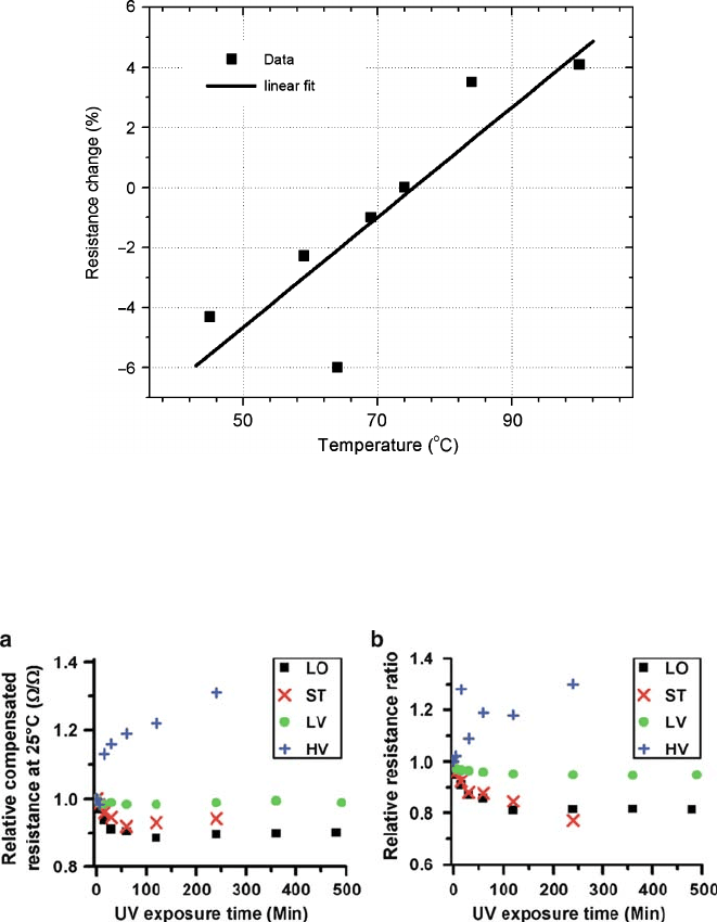
2 Metal-Insulator Transition in Thin Film Vanadium Dioxide 67
Fig. 2.12 The resistance change of a vanadium oxide thin (60 nm) film after the film was exposed
to UV radiation. The UV light affects only a few nm layer near the surface of the film [46], i.e., a
small fraction of the whole film. The observed clear resistance difference outlined by a straight line
fit evidences a significant change in the electrical resistance of the UV-affected material demon-
strating the possibility to control the oxidation process with UV radiation. (From Ruzmetov et al.
[24] with permission. Copyright (2007) by American Institute of Physics)
Fig. 2.13 The effect of UV irradiation on electrical parameters of vanadium oxide films exhibit-
ing MIT: ST stoichiometric VO
2
, LO low oxygen excess, LV and HV light and heavy vanadium
excess. (a) Relative change of resistance at 25
ı
C.R
r25
/;(b) Ratio of relative resistances at 25 and
100
ı
C;R
r25
=R
r100
. (From Ko et al. [47] with permission. Copyright (2008) by American Institute
of Physics)
upon UV irradiation. The relative resistance ratio below and above MIT can be
noticeably affected by UV as well (Fig. 2.13b). The relative resistance ratio was
defined in [47]as
