Ramanathan Sh. (Ed.) Thin Film Metal-Oxides: Fundamentals and Applications in Electronics and Energy
Подождите немного. Документ загружается.

78 D. Ruzmetov and S. Ramanathan
In Fig. 2.18, the peaks near 1 eV, above the O-2p peak are due to the V-3d bands
[16,50,60,67]. We see qualitatively the same behavior of the spectra as was reported
for bulk VO
2
with photon excitation of 21 eV [68] – a peak around 1 eV present in
both metallic and insulating phases and a weaker satellite appearing at the Fermi
level in the metallic VO
2
– with the difference that in our data the peaks are con-
siderably better resolved. The latter allows us to extract the precise peak positions
and widths by fitting to the measured data. The line shape of each peak employed
in the fitting is a numerical convolution of a Lorentzian with a Gaussian where the
latter represents the broadening due to the experimental instrument function. The
calculated spectra are shown in Fig. 2.18b by solid lines. The O-2p shoulder was
taken into account as an extra peak in the fitting, so, for example, the metallic phase
was fitted with an algebraic sum of three component peaks and a linear background.
The extracted peak parameters are discussed below: the single V-3d peak in the in-
sulating phase is located at 1.2 eV with linewidth of 1.0 eV. In the metallic phase the
doublet peak locations are 0.23 and 1.25 eV, linewidths being 0.76 and 1.5eV.
Photoemission studies on bulk VO
2
have shown well-resolved V-3d structure
with an unusual feature that the spectral weight was shifted mainly on the first peak
(at E
F
) in the metallic phase [50]. Such spectral weight ratio agreed with the calcu-
lations by Biermann et al. based on cluster dynamical mean field theory (CDMFT)
[50, 51]. In the spectra in Fig. 2.18, however, we see an opposite spectral weight
ratio, i.e., the peak at E
F
is at least three times less intense than the lower peak at
1.25 eV. It has been shown by Eguchi et al. that this ratio depends on the incident
photon energy [69], i.e., higher photon energies provide bulk sensitivity and the
spectra demonstrate higher DOS at the Fermi level. It is thus possible that the V-3d
spectra might be influenced by near-surface effects of the VO
2
film. Nevertheless,
the fact that we clearly see the closure of the band gap upon MIT in Fig. 2.18b
strongly suggests that the presented spectra describe the valence band structure of
VO
2
.
2.7 Optical Properties
Sharp changes of the electrical properties of VO
2
upon the MIT are accompanied
with the abrupt changes in the optical properties. Below we show the evolution of
the reflectance dispersion curves across the MIT and relate the changes of the optical
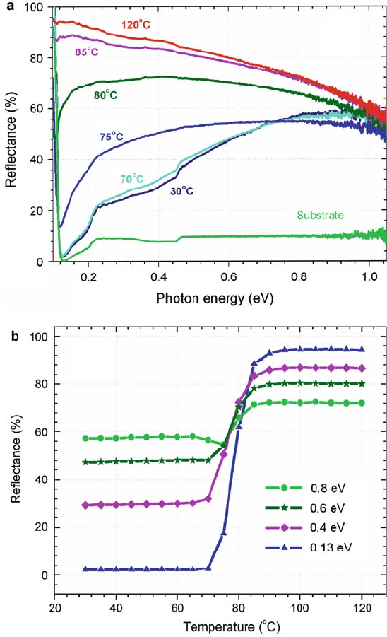
properties to electrical parameters. We demonstrate that the jump of the reflectivity
at the MIT can be as high as 92% (from 2 to 94%) at certain wavelengths.
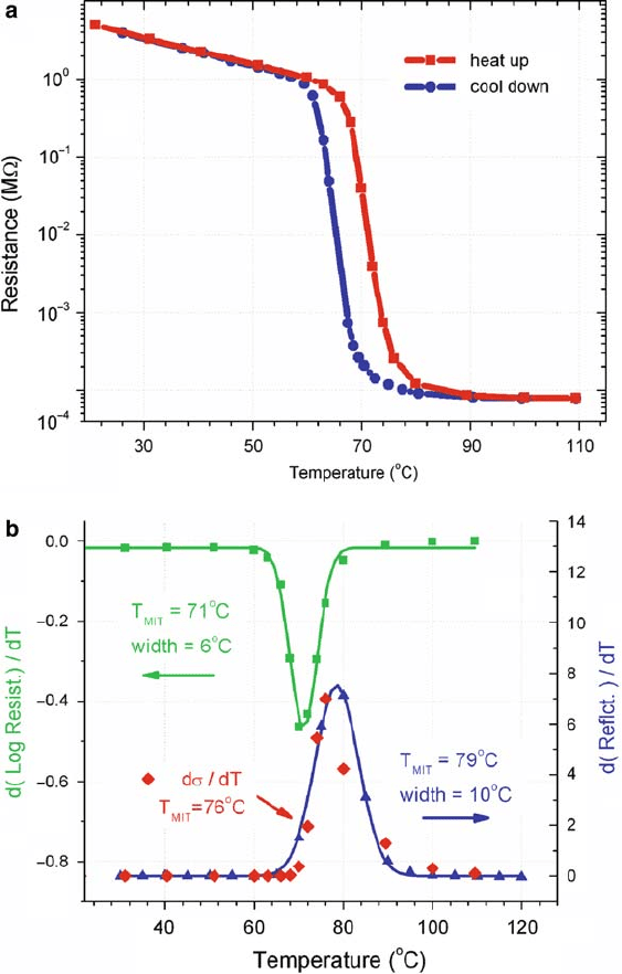
Figure 2.19a shows the electrical resistance plot from a thin film VO
2
sample.
The resistance change is over 4 orders of magnitude comparable to the sharpest
reported MIT in single crystals [7] and epitaxial films [9]. The point of the highest
gradient of this log R curve is usually taken to define the MIT temperature, T
MIT
.
Fig. 2.19b shows the derivative of log R curve, d.log R/=dT , fitted with a Gaussian.
The center and width of the Gaussian are 71 and 6
ı
C, respectively, and correspond
to conventionally defined T
MIT
and transition width
MIT
, respectively.
2 Metal-Insulator Transition in Thin Film Vanadium Dioxide 79
Fig. 2.19 Hundred-nanometer-thick VO
2
film on Al
2
O
3
substrate. (a) Electrical resistance .R/;
(b) Green squares and solid line connecting them – the temperature derivative of log R during
heating shown in (a) and a Gaussian fit to the data; red diamonds the derivative of the conductivity
.1=R/ corresponding to heating data in (a) on a linear scale; blue triangles the derivative of the
reflectance of 0.13 eV photons from Fig. 2.20b, blue line Gaussian fit. (From Ruzmetov et al. [16]
with permission. Copyright (2008) by the IOP Publishing Ltd)
80 D. Ruzmetov and S. Ramanathan
Fig. 2.20 (a) Infrared reflectance taken from VO
2
film as a function of incident photon energy
at different temperatures; (b) Reflectance change upon heating at selected photon energies. (From
Ruzmetov et al. [16] with permission. Copyright (2008) by the IOP Publishing Ltd)
The mid-infrared reflectance spectra from a VO
2
film on c-plane Al
2
O
3
substrate
are shown in Fig. 2.20. These optical measurements were done on the same film
whose electrical transition is shown in Fig. 2.19 allowing a direct comparison
2 Metal-Insulator Transition in Thin Film Vanadium Dioxide 81
between electrical and optical data [16]. The temperature dependence of reflectance
at selected incident photon energies is shown in Fig. 2.20b. One can see a sharp
increase in reflectance when the film is heated across the metal–insulator transition.
Larger magnitude of the reflectance switching occurs at lower photon energies. For
example, at h D 0:13 eV. D 9:54 m/ the reflectance switches from 2 to 94%
upon the MIT, which well exceeds the largest reported magnitudes of optical re-
flectance and transmittance switching in this material [4, 70–72]. One can see from
Fig. 2.20a that most of the change in the spectra with temperature occurs within
15
ı
C interval including the transition temperature. The magnitude of the switch-
ing seen in Fig. 2.20b is monotonically decreasing with increasing photon energy,
while the transition interval remains the same 15
ı
C. The sharp slopes at MIT and
the flat portion of the curves below and above the transition are potentially valuable
for developing applications such as optical switches.
An interesting feature is observed in the 0.8 eV reflectance curve in Fig. 2.20b.
There is a distinct decrease of the reflectance at the onset of MIT near 75
ı
C. This
feature is also seen in the spectra in Fig. 2.20a. The 75
ı
C curve is lower than
70
ı
C in the energy interval from 0.75 up to 1 eV. It is worthwhile to note that the
value of the band gap in semiconducting (monoclinic lattice) VO
2
is 0:6–0:7 eV
[60, 64]. The inelastic scattering involving excitations across the band gap become
possible in the h range 0.75–1eV where a decrease in reflectance is observed.
However this may not directly explain the temperature dependence of the effect,
i.e., its appearance right near the T
MIT
. More likely, this phenomenon may be sim-
ilar to the critical opalescence in liquid–vapor phase transitions. It has been shown
that the semiconductor-to-metal phase transition in VO
2
occurs percolatively: first
metallic puddles nucleate, then their size grows until the metallic phase percolates
throughout the whole material [58, 70]. During the transition, there is coexistence
of spatially separate metallic and insulating phases. When the wavelength of the in-
cident radiation is comparable with the characteristic size of the metallic puddles,
enhanced scattering is expected which would lead to the decline in reflection. The
typical size of the metallic puddles in the middle of the transition can be estimated
to be 1–2m[58]. Further growth of the metallic puddles results in complete merg-
ing of the metallic phase and consequently an increase of the reflectance. Enhanced
scattering is then expected at D 1–2m .PE D 1:2 0:6 eV/ in agreement with
our observation.
Another interesting feature can be noted from a comparison of the electrical and
optical MIT characteristics shown in Fig. 2.19b. The derivative of the reflectance
is fitted with a Gaussian to determine the optical transition temperature and width.
If one assumes the MIT temperature to be the highest gradient point in the log of
resistance curve, then the T
MIT
would be equal to 71
ı
C, which is 8
ı
C apart from the
highest gradient point in the reflectance data, 79
ı
C. The maximum error between the
sample temperature readings in electrical and optical experiments was determined
to be less than 2
ı
C and cannot explain the mentioned 8
ı
C difference. To understand
the origin of the discrepancy we have plotted in Fig. 2.19b the derivative of the
electrical conductance d=dT upon heating calculated from the data in Fig. 2.2a
. D 1=R/. We found that the point of highest gradient of the conductance, 76
ı
C,
82 D. Ruzmetov and S. Ramanathan
is closer to the optical transition point, 79
ı
C, and, more importantly, that the interval
of the conductance change overlaps with the interval of the optical transition. The
latter indicates that the film’s optical characteristics can be better described as a
direct function of conductance, or consequently the free carrier density, and the
center of the reflectance transition occurs at the threshold conductance value close
to the highest gradient of .T/.
The remarkably large switching of the optical properties described above, the
fact that the material is in thin film form, which can potentially be integrated into
electronic and optical devices, and relatively simple way of the synthesis of our
polycrystalline films (DC sputtering as opposed to epitaxial methods of film growth)
make these results to be of potential significance to switching technologies.
2.8 Magneto-Transport
As it is discussed in Sect. 5, there are a number of theoretical models developed
describing MIT in VO
2
. The carrier density is a critical parameter in some of those
models (e.g., Mott theory [37]) and is an important reference parameter in the oth-
ers (e.g., for comparison with the predictions of the electronic occupancies of the
molecular orbitals). The knowledge of the carrier density across MIT is important
in order to distinguish between competing theories and understand the origin of the
phase transition.
Early Hall effect measurements in VO
2
showed that electrons were predominant
carriers on the both sides of the MIT [66, 73–76]. The values of the electron den-
sity reported by research groups could differ by 2 orders of magnitude both in the
semiconducting phase at room temperature [66, 73, 75] and high-T metallic phase
[73, 75]. As mentioned in the literature [66, 77], the Hall effect measurements in
VO
2
is a challenging task due to the following difficulties: low Hall mobility, high
carrier density resulting in low Hall voltage, and unusually large amount of noise
ascribed to be due to the strain present in the sample arising from the discontinu-
ous lattice transformation at the structural phase transition (SPT). Carrier density
determination in high-quality vanadium oxide films is important, given the recent
interest in exploiting the Mott transition for computational elements that may over-
come limitations due to Si CMOS scaling [78].
We now discuss recent results on Hall and magnetoresistance measurements in
thin film VO
2
in DC magnetic field of up to 12T [77]. The temperature depen-
dence of the electrical resistivity, carrier density, and Hall mobility across the MIT
is shown below. The measured n-type conductance in the semiconducting phase is
consistent with recent photoemission spectroscopy results [16]. The novelty and im-
portance of these results are that the high field measurement technique allowed for
reliable Hall coefficient determination in both semiconducting and metallic states of
high quality thin film VO
2
.
VO
2
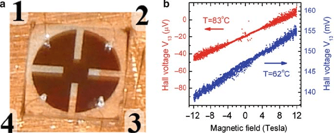
film (100-nm thick) on a sapphire substrate was photo-lithographically pat-
terned into a clover-leaf shape for van der Pauw measurements (Fig. 2.21a) [77].
2 Metal-Insulator Transition in Thin Film Vanadium Dioxide 83
Fig. 2.21 (a)VO
2
sample mounted on a copper base and set up for Hall measurements. Dark
clover-leaf pattern is a VO
2
film on transparent square sapphire substrate of 1 cm 1 cm size.
(b) The Hall voltage V
13
in the metallic (upper red dot group) and semiconducting (lower blue
dot group) state. (From Ruzmetov et al. [77] with permission. Copyright (2009) by the American
Physical Society)
The sample was silver paste mounted on a copper block equipped with a resistive
heater. This custom made setup with LakeShore 340 temperature controller insured
sample temperature stability within 0:05
ı
C, which proved to be a necessary require-
ment since the sample resistance exponentially varied with temperature. Gold wires
were indium-soldered to the sample. Another wiring method where a second layer
of photo-lithography was used to connect 15-m-wide thin film gold leads to the
VO
2
pattern yielded similar results. Electrical measurements on the sample were
done with a DC current source and voltmeter. The copper block with the sample was
placed inside a room temperature bore of a 14T cryogen-free magnet. Constant cur-
rent I
24
was set through the sample. The current magnitude was set to maximum
before the current heating effects became present and varied from 35 Aat33
ı
Cto
120 Aat64
ı
C in the semiconducting phase and up to 10 mA in the metallic phase.
Hall voltage V
13
was measured while the magnetic field was continuously ramped
0 ! 12T !12T ! 0 at a preset temperature. The resistivity was measured
by van der Pauw method and calculated by solving numerically the transcendental
equation (1) in [79].
In the magneto-transport measurements on the 12T apparatus [77], the tempera-
ture was incrementally increased through the MIT. An example of the Hall voltage
curves in semiconducting and metallic phases is shown in Fig. 2.21b. Hall re-
sults are interpreted within a single band model, so that the slopes of the V
H
.B/
curves were used to extract Hall carrier densities using the equation (SI units):
n D IB=.V
H
ed/,whereI D I
24
is the current through the sample, B – magnetic
flux density directed perpendicular to the sample plane, V
H
D V
13
– Hall voltage,
e D 1:60 10
19
C;dD 10
7
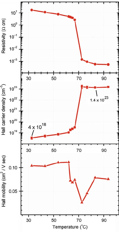
m – film thickness. The measured resistivity and
carrier density for the thin film VO
2
sample are presented in Fig. 2.22.
The resistivity experiences a drop of over 3 orders of magnitude at the transition
temperature T
MIT
D 70
ı
C, which is characteristic to vanadium dioxide. Together
84 D. Ruzmetov and S. Ramanathan
Fig. 2.22 Electron transport properties of a thin film VO
2
on an Al
2
O
3
substrate measured by
12T sweeping field apparatus. The Hall coefficient sign corresponds to electrons as the dominant
current carriers. (From Ruzmetov et al. [77] with permission. Copyright (2009) by the American
Physical Society)
2 Metal-Insulator Transition in Thin Film Vanadium Dioxide 85
with the results of the X-ray diffraction analysis [77] this demonstrates the high
quality and stoichiometry of the synthesized VO
2
films. The mobility D 1=.e n /
was determined from known resistivity and carrier density n andplottedinthe
bottom panel of Fig. 2.22. Positive magnetoresistance, i.e., a resistance increase
upon application of magnetic field, was measured in the semiconducting phase at
room temperature. Specifically, the magnetoresistance is R=R D .0:09 ˙0:02/%
in the ˙12Tfieldat26
ı
C, where R D V
13
=I
13
(in notations of Fig. 2.21a).
One can see in Fig. 2.22 that the Hall electron density increases by 4 orders of
magnitude from 1:1 10
19
cm
3
at 64
ı
Cto1:7 10
23
cm
3
at 75
ı
C upon the MIT.
The increase of the number of carriers accounts almost entirely for the decrease of
electrical resistance, which is also manifested in the small change in the mobility .
The fact that in the Hall measurements there appear to be more than one itinerant
carrier per V ion may be explained by the presence of two types of conduction,
n- and p-type, with electrons being the majority carriers [12].
2.9 Devices
More evidence is emerging ascribing the metal–insulator transition in VO
2
to be
a Mott transition [37]. In the Mott picture, the insulating state is achieved due to
the correlations between itinerant carriers [80]. The free carrier density is a key pa-
rameter that, upon the change of some external parameter such as temperature or
electric field, increases to a certain critical value causing the transition to metallic
state. Once the Coulomb repulsion between the electrons is overcome, further in-
crease of the carrier density occurs continuously. The fact that the MIT is activated
by the carrier density makes these materials promising for applications. The carrier
density in conventional semiconductors can be readily manipulated, for example,
by means of electric field or photo-excitation. There are a number of device con-
figurations allowing efficient carrier density control in a semiconductor channel that
are already being utilized in modern electronics. Making use of those configurations
and device schemes to develop devices that show explicitly that the MIT in VO
2
can
be induced solely by means of carrier density manipulation is a big challenge on the
way toward incorporating VO
2
materials in novel applications in electronics.
It has been found by a number of researchers that the application of sufficiently
high voltage across a two-terminal VO
2
device induces a metal–insulator transition
even if the sample is kept at room temperature [57, 81–83]. In early reports [81],
the MIT switching was explained by the Joule heating of the VO
2
material over the
T
MIT
by the current flowing through the two-terminal device. In some recent reports,
the switching is argued to be due to the electric field (not thermally)-induced MIT
in accordance to the Mott theory [83].
B.-J. Kim et al. performed electrical measurements on two-terminal VO
2
de-
vices consisting of a thin (100 nm) film VO
2
stripe contacted with Ni electrodes
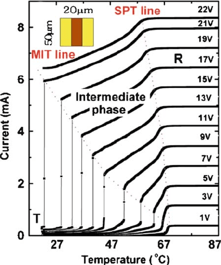
on both sides [84]. The device dimensions are shown in the inset of Fig. 2.23.In
the experiments of B.-J. Kim et al. [84], the temperature dependence of the current
86 D. Ruzmetov and S. Ramanathan
Fig. 2.23 The temperature dependence of a current through a two-terminal VO
2
device (inset)
at different applied voltages. At higher applied voltages the current jump corresponding to MIT
shifts to lower temperatures. (From Kim et al. [84] with permission. Copyright (2007) by American
Institute of Physics)
through the device was measured at different applied voltages ranging from 1 to
22 V (Fig. 2.23). At a small applied voltage of 1 V, a jump in the current due to
MIT is observed near 67
ı
C, which is close to the conventional MIT temperature in
single crystal (T
MIT
D 68
ı
C[12]) and thin film VO
2
(T
MIT
D 71
ı
C, see Fig. 2.19).
At higher applied voltages the current jump occurs at lower temperatures. This ef-
fect is explained by an electric field-induced metal–insulator transition (MIT): the
electric field produced by an applied voltage favors the MIT so that at higher volt-
ages lower temperature is sufficient to trigger the phase transition [84]. According
to B.-J Kim et al., the field-assisted transition to metallic state is not necessarily ac-
companied by the structural phase transition (SPT), i.e., lattice transformation from
monoclinic to tetragonal structure. So that there is an intermediate metallic phase,
which remains to have monoclinic lattice. The current in this intermediate phase
continues to increase with temperature at constant applied voltage until the SPT
occurs. The temperature increase beyond SPT results in almost constant saturated
current, which allows delimiting the boundaries of all three phases in the graph
of Fig. 2.23: monoclinic semiconductor phase, monoclinic metallic (intermediate
phase), and tetragonal metallic phase. Further arguments in favor of the intermediate
phase and the separation of MIT and SPT can be found elsewhere [37].
2 Metal-Insulator Transition in Thin Film Vanadium Dioxide 87
One needs to consider carefully the electric field-induced MIT in two-terminal
devices. The current that passes through the device causes Joule heating that can
raise the temperature of VO
2
toward T
MIT
. The latter would result in conventional
temperature activated MIT rather than field induced one. If there is nonuniform con-
ductance in the VO
2
film, then the applied voltage may raise the temperature of VO
2
in a narrow filament of the material causing thermal MIT in the filament. The rest of
the film that does not participate in conduction will remain at low temperature. In or-
der to eliminate the possibility of this and similar scenarios more experiments need
to be considered. Three-terminal devices are especially of interest since an electric
field induced by the third terminal (gate) causes only minimal leakage current and,
consequently, heating.
There are only a few reports on the measurements of three-terminal VO
2
devices
consisting of a source, drain, and gate [57, 85]. The application of an electric field
in VO
2
through a gate seems to shift the critical source–drain field that induces the
MIT. However, the interpretation of the field effect is complicated by the fact that the
same polarity of the gate voltage may either increase or decrease the critical source–
drain field [57]. Careful studied of three-terminal VO
2
devices are still desirable in
order to clarify the effect of the electric field induced by a gate on the transport
properties of VO
2
.
There have been attempts to discriminate heating and field effects in two-terminal
devices by means of time-resolved measurements. The switching time of the MIT
was measured and arguments were given that thermally activated switching would
occur at a slower rate than it was observed leaving the electric field induced MIT as
the mechanism of the phase transition [86].
Another important type of VO
2
devices to be studied is two-terminal devices
with the C urrent flowing P erpendicular to sample P lane (CPP geometry) as op-
posed to in-plane devices (Current InsamplePlane or CIP geometry) described in
Fig. 2.23. Ko et al. performed experiments comparing electron transport in CPP and
CIP geometries and demonstrated that the MIT can be induced by application of
electric field across a thin VO
2
film [87]. Experiments on devices in CPP configu-
ration are important from the scientific point of view since MIT in VO
2
is probed
on the nanoscale that is equivalent to the thickness of the VO
2
thin film. Also CPP
devices are attractive from the perspective of potential applications in electronics
because CPP geometry allows high device density.
In the experiments of Ko et al. [87] palladium electrodes (0:5 mm 0:5 mm
squares, 200-nm thick) were placed on top of a 150-nm thick VO
2
film deposited
on a conductive silicon substrate. The latter was used as the bottom electrode, so
that a voltage was applied across the thickness of the film and the current was mea-
sured (Fig. 2.24). The current curves at temperatures below 55
ı
C feature jumps near
2 V bias could be due to the electric field assisted MIT (E-MIT). An abrupt current
change in Fig. 2.24 seen in the direction of a constant voltage (e.g., 0.6 V) between
70 and 75
ı
C curves corresponds to a conventional thermally induced MIT (T-MIT).
The convergenceof the high .T > T
MIT
70
ı
C/ and low temperature curves at high
fields indicate that both effects, T-MIT and E-MIT, produce the transition to a similar
metallic phase of the VO
2
material. This conclusion makes alternative explanations
