Power electronic handbook
Подождите немного. Документ загружается.

34 Control Methods for Switching Power Converters 937
converter circuit, Eq. (34.4) or (34.5):
˙x =
[
A
1
δ
(
t
)
+A
2
(
1−δ
(
t
))
]
x+
[
B
1
δ
(
t
)
+B
2
(
1−δ
(
t
))
]
u
y =
[
C
1
δ
(
t
)
+C
2
(
1−δ
(
t
))
]
x+
[
D
1
δ
(
t
)
+D
2
(
1−δ
(
t
))
]
u
(34.4)
˙x = A
S
x +B
S
u
y = C
S
x +D
S
u
(34.5)
where A
S
=
[
A
1
δ
(
t
)
+A
2
(
1 −δ
(
t
))
]
, B
S
=
[
B
1
δ
(
t
)
+
B
2
(
1 −δ
(
t
))
]
, C
S
=
[
C
1
δ
(
t
)
+C
2
(
1 −δ
(
t
))
]
, and D
S
=
[
D
1
δ
(
t
)
+D
2
(
1 −δ
(
t
))
]
.
34.2.2.2 State-space Averaged Model
Since the state variables of the x vector are continuous,
using Eq. (34.4), with the initial conditions x
1
(0) = x
2
(T),
x
2
(δ
1
T) = x
1
(δ
1
T), and considering the duty cycle δ
1
as the
average value of δ(t), the time evolution of the converter state
variables can be obtained, integrating Eq. (34.4) over the inter-
vals 0 ≤ t ≤ δ
1
T and δ
1
T ≤ t ≤ T , although it often requires
excessive calculation effort. However, a convenient approxi-
mation can be devised, considering λ
max
, the maximum of the
absolute values of all eigenvalues of A (usually λ
max
is related
to the cutoff frequency f
c
of an equivalent low-pass filter with
f
c
1/T ). For λ
max
T 1, the exponential matrix (or state
transition matrix) e
At
= I + At + A
2
t
2
/2 +···+A
n
t
n
/n!,
where I is the identity or unity matrix, can be approxi-
mated by e
At
≈ I + At . Therefore, e
A
1
δ
1
t
· e
A
2
(
1−δ
1
)
t
≈
I +
[
A
1
δ
1
+A
2
(1 −δ
1
)
]
t. Hence, the solution over the period
T, for the system represented by Eq. (34.4), is found to be:
x
(
T
)
∼
=
e
[
A
1
δ
1
+A
2
(
1−δ
1
)
]
T
x
1
(
0
)
+
T
0
e
[
A
1
δ
1
+A
2
(
1−δ
1
)
]
(
T−τ
)
[
B
1
δ
1
+B
2
(
1 −δ
1
)
]
udτ
(34.6)
This approximate response of Eq. (34.4) is identical to the
exact response obtained from the nonlinear continuous time-
invariant state-space model (34.7), supposing that the average
Q
1
V
DC
V
DC
v
Li
−v
0
v
0
i
L
D
1
L
i
C
0
R
0
Q
1
v
Li
i
L
T2Tt
D
1
on
on
v
0
+
+
−
−
+−
(a) (b)
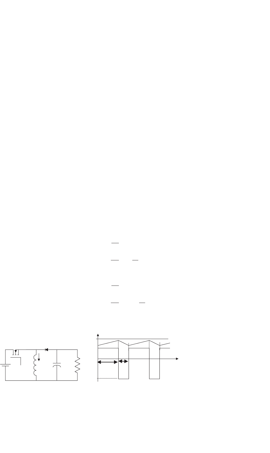
FIGURE 34.1 (a) Basic circuit of the buck–boost dc/dc converter and (b) ideal waveforms.
values of x, denoted ¯x, are the new state variables, and consid-
ering δ
2
= 1 −δ
1
. Moreover, if A
1
A
2
= A
2
A
1
, the approxi-
mation is exact.
˙
¯x =
[
A
1
δ
1
+A
2
δ
2
]
¯x +
[
B
1
δ
1
+B
2
δ
2
]
¯u
¯y =
[
C
1
δ
1
+C
2
δ
2
]
¯x +
[
D
1
δ
1
+D
2
δ
2
]
¯u
(34.7)
For λ
max
T 1, the model (34.7), often referred to as
the state-space averaged model, is also said to be obtained by
“averaging” Eq. (34.4) over one period, under small ripple and
slow variations, as the average of products is approximated by
products of the averages. Comparing Eq. (34.7) to Eq. (34.1),
the relations (34.8), defining the state-space averaged model,
are obtained.
A =
[
A
1
δ
1
+A
2
δ
2
]
; B =
[
B
1
δ
1
+B
2
δ
2
]
;
C =
[
C
1
δ
1
+C
2
δ
2
]
; D =
[
D
1
δ
1
+D
2
δ
2
]
(34.8)
E
XAMPLE 34.1 State-space models for the buck–
boost dc/dc converter
Consider the simplified circuitry of the buck–boost con-
verter of Fig. 34.1 switching at f
s
= 20 kHz (T = 50 µs)
with V
DCmax
= 28 V, V
DCmin
= 22 V, V
o
= 24 V,
L
i
= 400 µH, C
o
= 2700 µF, R
o
= 2 .
The differential equations governing the dynamics of
the state vector x = [i
L
, v
o
]
T
(
T
denotes the transpose
of vectors or matrices) are:
L
i
di
L
dt
= V
DC
C
o
dv
o
dt
=−
v
o
R
o
for 0 ≤ t ≤ δ
1
T (δ
(
t
)
= 1,
Q
1
is on and D
1
is off)
(34.9)
L
i
di
L
dt
=−v
o
C
o
dv
o
dt
= i
L
−
v
o
R
o
for δ
1
T ≤ t ≤ T (δ
(
t
)
= 1,
Q
1
is off and D
1
is on)
(34.10)
938 J. F. Silva and S. F. Pinto
Comparing Eqs. (34.9) and (34.10) to Eqs. (34.2)
and (34.3) and considering y =[v
o
, i
L
]
T
, the following
matrices can be identified:
A
1
=
00
0 −1/
(
R
o
C
o
)
; A
2
=
0 −1/L
i
1/C
o
−1/
(
R
o
C
o
)
;
B
1
=
[
1/L
i
,0
]
T
; B
2
=
[
0, 0
]
T
; u =
[
V
DC
]
;
C
1
=
01
10
; C
2
=
01
10
;
D
1
=
[
0, 0
]
T
; D
2
=
[
0, 0
]
T
From Eqs. (34.4) and (34.5), the switched state-space
model of this switching converter is
˙
i
L
˙v
o
=
0 −
1 −δ(t)
/L
i
1 −δ(t)
/C
o
−1/(R
o
C
o
)
i
L
v
o
+
δ(t)/L
i
0
V
DC
v
o
i
L
=
01
10
i
L
v
o
+
0
0
[V
DC
]
(34.11)
Now, applying Eq. (34.7), Eqs. (34.12) and (34.13)
can be obtained:
˙
¯
i
L
˙
¯v
o
=
00
0 −1/R
o
C
o
δ
1
+
0 −1/L
i
1/C
o
−1/R
o
C
o
δ
2
×
¯
i
L
¯v
o
+
1/L
i
0
δ
1
+
0
0
δ
2
¯
V
DC
(34.12)
¯v
o
¯
i
L
=
01
10
δ
1
+
01
10
δ
2
¯
i
L
¯v
o
+
0
0
δ
1
+
0
0
δ
2
¯
V
DC
(34.13)
From Eqs. (34.12) and (34.13), the state-space aver-
aged model, written as a function of δ
1
,is
˙
¯
i
L
˙
¯v
o
=
0 −1−δ
1
/L
i
1−δ
1
/C
o
−1/R
o
C
o
¯
i
L
¯v
o
+
δ
1
/L
i
0
¯
V
DC
(34.14)
¯v
o
¯
i
L
=
01
10
¯
i
L
¯v
o
+
0
0
¯
V
DC
(34.15)
The eigenvalues s
bb
1,2
, or characteristic roots of A, are
the roots of |sI−A|. Therefore:
s
bb
1,2
=
−1
2R
o
C
o
±
1
4
(
R
o
C
o
)
2
−
(
1 −δ
1
)
2
L
i
C
o
(34.16)
Since λ
max
is the maximum of the absolute values of all the
eigenvalues of A, the model (34.14, 34.15) is valid for switching
frequencies f
s
(f
s
= 1/T ) that verify λ
max
T 1. Therefore,
as T 1/λ
max
, the values of T that approximately verify
this restriction are T 1/max(|s
bb
1,2
|). Given this buck–boost
converter data, T 2 ms is obtained. Therefore, the converter
switching frequency must obey f
s
max(|s
f 1,2
|), implying
switching frequencies above, say, 5 kHz. Consequently, the
buck–boost switching frequency, the inductor value, and the
capacitor value were chosen accordingly.
This restriction can be further used to discuss the maximum
frequency ω
max
for which the state-space averaged model is
still valid, given a certain switching frequency. As λ
max
can
be regarded as a frequency, the preceding constraint brings
ω
max
2πf
s
, say ω
max
< 2πf
s
/10, which means that the state-
space averaged model is a good approximation at frequencies
under one-tenth of the power converter switching frequency.
The state-space averaged model (34.14, 34.15) is also the
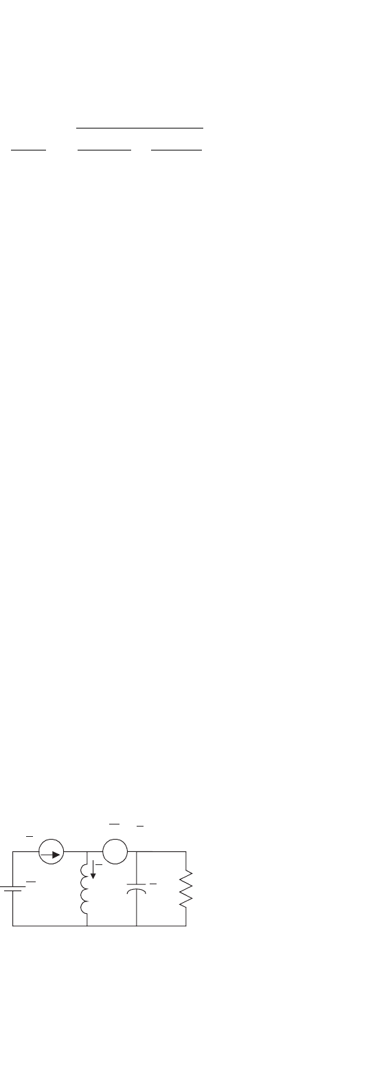
state-space model of the circuit represented in Fig. 34.2. Hence,
this circuit is often named “the averaged equivalent circuit”
of the buck–boost converter and allows the determination,
under small ripple and slow variations, of the average equiv-
alent circuit of the converter switching cell (power transistor
plus diode).
The average equivalent circuit of the switching cell
(Fig. 34.3a) is represented in Fig. 34.3b and emerges directly
from the state-space averaged model (34.14, 34.15). This
equivalent circuit can be viewed as the model of an “ideal
transformer” (Fig. 34.3c), whose primary to secondary ratio
(v
1
/v
2
) can be calculated applying Kirchhoff’s voltage law to
obtain −v
1
+ v
s
− v
2
= 0. As v
2
= δ
1
v
s
, it follows that
v
1
= v
s
(1 − δ
1
), giving (v
1
/v
2
) = (1 − δ
1
)/δ
1
. The same ratio
could be obtained beginning with i
L
= i
1
+ i
2
, and i
1
= δ
1
i
L
(Fig. 34.3b) which gives i
2
= i
L
(1 −δ
1
) and (i
2
/i
1
) = δ
2
/δ
1
.
The average equivalent circuit concept, obtained from
Eq. (34.7) or Eqs. (34.14) and (34.15), can be applied to
other switching converters, with or without a similar switch-
ing cell, to obtain transfer functions or to computer simulate
δ
1
i
L
L
i
C
0
v
0
R
0
i
L
δ
1
(V
DC
+v
0
)
+
+
−
−
V
DC
+−
FIGURE 34.2 Equivalent circuit of the averaged state-space model of
the buck–boost converter.

34 Control Methods for Switching Power Converters 939
V
DC
δ
1
i
L
δ
1
v
s
v
s
v
s
Q
1
i
L
i
L
i
1
i
2
i
L
v
2
v
1
D
1
−v
0
v
s
+
+−
−
−
−
+
+
+
−
+
δ
2
:δ
1
−
(b) (c)(a)
FIGURE 34.3 Average equivalent circuit of the switching cell: (a) switching cell; (b) average equivalent circuit; and (c) average equivalent circuit
using an ideal transformer.
the converter average behavior. The average equivalent circuit
of the switching cell can be applied to converters with the
same switching cell operating in the continuous conduction
mode. However, note that the state variables of Eq. (34.7)
or Eqs. (34.14) and (34.15) are the mean values of the con-
verter instantaneous variables and, therefore, do not represent
their ripple components. The inputs of the state-space aver-
aged model are the mean values of the converter inputs over
one switching period.
34.2.2.3 Linearized State-space Averaged Model
Since the converter outputs ¯y must be regulated actuating
on the duty cycle δ(t ), and the converter inputs ¯u usually
present perturbations due to the load and power supply varia-
tions. State variables are decomposed in small ac perturbations
(denoted by “∼”) and dc steady-state quantities (represented
by uppercase letters). Therefore:
¯x = X +˜x
¯y = Y +˜y
¯u = U +˜u
δ
1
=
1
+
˜
δ
δ
2
=
2
−
˜
δ
(34.17)
Using Eq. (34.17) in Eq. (34.7) and rearranging terms, we
obtain:
˙
˜x =
[
A
1
1
+A
2
2
]
X+
[
B
1
1
+B
2
2
]
U
+
[
A
1
1
+A
2
2
]
˜x+
[
(
A
1
−A
2
)
X+
(
B
1
−B
2
)
U
]
˜
δ
+
[
B
1
1
+B
2
2
]
˜u+
[
(
A
1
−A
2
)
˜x+
(
B
1
−B
2
)
˜u
]
˜
δ
(34.18)
Y+˜y =
[
C
1
1
+C
2
2
]
X+
[
D
1
1
+D
2
2
]
U
+
[
C
1
1
+C
2
2
]
˜x+
[
(
C
1
−C
2
)
X+
(
D
1
−D
2
)
U
]
˜
δ
+
[
D
1
1
+D
2
2
]
˜u+
[
(
C
1
−C
2
)
˜x+
(
D
1
−D
2
)
˜u
]
˜
δ
(34.19)
The terms
[
A
1
1
+A
2
2
]
X +
[
B
1
1
+B
2
2
]
U and
[
C
1
1
+C
2
2
]
X +
[
D
1
1
+D
2
2
]
U, respectively from
Eqs. (34.18) and (34.19), represent the steady-state behav-
ior of the system. As in steady state
˙
X = 0, the following
relationships hold:
0 =
[
A
1
1
+A
2
2
]
X +
[
B
1
1
+B
2
2
]
U (34.20)
Y =
[
C
1
1
+C
2
2
]
X +
[
D
1
1
+D
2
2
]
U (34.21)
Neglecting higher order terms ([(A
1
−A
2
) ˜x +(B
1
−B
2
) ˜u]
˜
δ ≈ 0) of Eqs. (34.18) and (34.19), the linearized small-signal
state-space averaged model is
˙
˜x =
[
A
1
1
+A
2
2
]
˜x +
[
(
A
1
−A
2
)
X +
(
B
1
−B
2
)
U
]
˜
δ
+
[
B
1
1
+B
2
2
]
˜u
˜y =
[
C
1
1
+C
2
2
]
˜x +
[
(
C
1
−C
2
)
X +
(
D
1
−D
2
)
U
]
˜
δ
+
[
D
1
1
+D
2
2
]
˜u
(34.22)
or
˙
˜x = A
av
˜x +B
av
˜u +
[
(
A
1
−A
2
)
X +
(
B
1
−B
2
)
U
]
˜
δ
˜y = C
av
˜x +D
av
˜u +
[
(
C
1
−C
2
)
X +
(
D
1
−D
2
)
U
]
˜
δ
(34.23)
with
A
av
=
[
A
1
1
+A
2
2
]
B
av
=
[
B
1
1
+B
2
2
]
C
av
=
[
C
1
1
+C
2
2
]
D
av
=
[
D
1
1
+D
2
2
]
(34.24)
34.2.3 Converter Transfer Functions
Using Eq. (34.20) in Eq. (34.21), the input U to output
Y steady-state relations (34.25), needed for open-loop and
feedforward control, can be obtained.

940 J. F. Silva and S. F. Pinto
Y
U
=−C
av
A
−1
av
B
av
+D
av
(34.25)
Applying Laplace transforms to Eq. (34.23) with zero initial
conditions, and using the superposition theorem, the small-
signal duty-cycle
˜
δ to output ˜y transfer functions (34.26) can
be obtained considering zero line perturbations (˜u = 0).
˜y(s)
˜
δ(s)
= C
av
[
sI −A
av
]
−1
[
(
A
1
−A
2
)
X +
(
B
1
−B
2
)
U
]
+
[
(
C
1
−C
2
)
X +
(
D
1
−D
2
)
U
]
(34.26)
The line to output transfer function (or audio susceptibility
transfer function) (34.27) is derived using the same method,
considering now zero small-signal duty-cycle perturbations
(
˜
δ = 0).
˜y(s)
˜u(s)
= C
av
[
sI −A
av
]
−1
B
av
+D
av
(34.27)
E
XAMPLE 34.2 Buck–Boost dc/dc converter transfer
functions
From Eqs. (34.14) and (34.15) of Example 34.1 and
Eq. (34.23), making X =[I
L
, V
o
]
T
, Y =[V
o
, I
L
]
T
,
and U =[V
DC
], the linearized state-space model of the
buck–boost converter is
˙
˜
i
L
˙
˜v
o
=
0 −1−
1
/L
i
1−
1
/C
o
−1/R
o
C
o
˜
i
L
˜v
o
+
1
/L
i
0
[˜v
DC
]
+
0
˜
δ/L
i
−
˜
δ/C
o
0
I
L
V
o
+
V
DC
/L
i
0
[
˜
δ]
˜v
o
˜
i
L
=
01
10
˜
i
L
˜v
o
+
0
0
[˜v
DC
]
(34.28)
From Eqs. (34.24) and (34.28), the following matrices
are identified:
A
av
=
0 −(1 −
1
)/L
i
1 −
1
/C
o
−1/R
o
C
o
; B
av
=
1
/L
i
0
;
C
av
=
01
10
; D
av
=
0
0
(34.29)
The averaged linear equivalent circuit, resulting from
Eq. (34.28) or from the linearization of the averaged
equivalent circuit (Fig. 34.2) derived from Eqs. (34.14)
and (34.15), now includes the small-signal current
source
˜
δI
L
in parallel with the current source
1
˜
i
L
, and
the small-signal voltage source
˜
δ
(
V
DC
+V
o
)
in series
with the voltage source
1
(˜v
dc
+˜v
o
). The supply voltage
source
¯
V
DC
is replaced by the voltage source ˜v
DC
.
Using Eq. (34.29) in Eq. (34.25), the input U to output
Y steady-state relations are:
I
L
V
DC
=
1
R
o
(
1
−1
)
2
(34.30)
V
o
V
DC
=
1
1 −
1
(34.31)
These relations are the well-known steady-state trans-
fer relationships of the buck–boost converter [2, 5, 6].
For open-loop control of the V
o
output, knowing the
nominal value of the power supply V
DC
and the required
V
o
, the value of
1
can be off-line calculated from
Eq. (34.31) (
1
= V
o
/(V
o
+ V
DC
)). A modulator such
as that described in Section 34.2.4, with the modula-
tion signal proportional to
1
, would generate the signal
δ(t). The open-loop control for fixed output voltages is
possible, if the power supply V
DC
is almost constant
and the converter load does not change significantly. If
the V
DC
value presents disturbances, then the feedfor-
ward control can be used, calculating
1
on-line, so that
its value will always be in accordance with Eq. (34.31).
The correct V
o
value will be attained at steady state,
despite input-voltage variations. However, because of
converter parasitic reactances, not modeled here (see
Example 34.3), in practice a steady-state error would
appear. Moreover, the transient dynamics imposed by
the converter would present overshoots, being often not
suited for demanding applications.
From Eq. (34.27), the line to output transfer functions
are:
˜
i
L
(s)
˜v
DC
(s)
=
1
(
1 +sC
o
R
o
)
s
2
L
i
C
o
R
o
+sL
i
+R
o
(
1 −
1
)
2
(34.32)
˜v
o
(s)
˜v
DC
(s)
=
R
o
1
(
1 −
1
)
s
2
L
i
C
o
R
o
+sL
i
+R
o
(
1 −
1
)
2
(34.33)
From Eq. (34.26), the small-signal duty-cycle
˜
δ to
output ˜y transfer functions are:
˜
i
L
(s)
˜
δ(s)
=
V
DC
(
1 +
1
+sC
o
R
o
)
/
(
1 −
1
)
s
2
L
i
C
o
R
o
+sL
i
+R
o
(
1 −
1
)
2
(34.34)
˜v
o
(s)
˜
δ(s)
=
V
DC
R
o
−sL
i
1
(
1 −
1
)
2
s
2
L
i
C
o
R
o
+sL
i
+R
o
(
1 −
1
)
2
(34.35)
These transfer functions enable the choice and
feedback-loop design of the compensation network.
Note the positive zero in ˜v
o
(s)/
˜
δ(s), pointing out a
34 Control Methods for Switching Power Converters 941
V
DC
Q
1
D
1
D
2
r
c
R
0
v
0
C
0
Q
1
D
1
on D
2
on
T2Tt
v
c
+
+
−
+
−
−
r
L
L
i
i
L
i
L
v
0
V
DC
v
AK2
n
(b)
n : 1
(a)
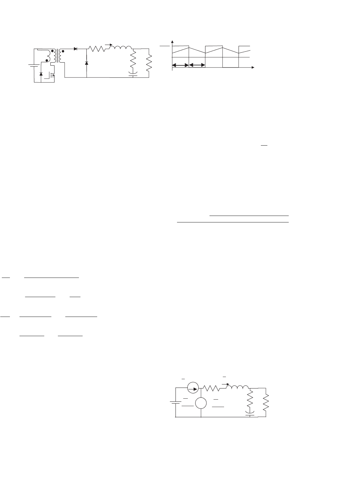
FIGURE 34.4 (a) Basic circuit of the forward dc/dc converter and (b) circuit main waveforms.
nonminimum-phase system. These equations could also
be obtained using the small-signal equivalent circuit
derived from Eq. (34.28), or from the linearized model
of the switching cell Fig. 34.3b, substituting the current
source δ
1
¯
i
L
by the current sources
1
˜
i
L
and
˜
δI
L
in par-
allel, and the voltage source δ
1
¯v
s
by the voltage sources
1
˜v
DC
+˜v
o
and
˜
δ
(
V
DC
+V
o
)
in series.
E
XAMPLE 34.3 Transfer functions of the forward
dc/dc converter
Consider the forward (buck derived) converter of
Fig. 34.4 switching at f
s
= 100 kHz (T = 10 µs) with
V
DC
= 300 V, n = 30, V
o
= 5V, L
i
= 20 µH,
r
L
= 0.01 , C
o
= 2200 µF, r
C
= 0.005 , R
o
= 0.1 .
Assuming x = [i
L
, v
C
]
T
, δ(t) = 1 when both Q
1
,D
1
are on and D
2
is off (0 ≤ t ≤ δ
1
T), δ(t) = 0 when both
Q
1
,D
1
are off and D
2
is on (δ
1
T ≤ t ≤ T ), the switched
state-space model of the forward converter, considering
as output vector y =[i
L
, v
o
]
T
,is
di
L
dt
=−
(
R
o
r
C
+R
o
r
L
+r
L
r
C
)
L
i
(
R
o
+r
C
)
i
L
−
R
o
L
i
(
R
o
+r
C
)
v
c
+
δ
(
t
)
n
V
DC
dv
C
dt
=
R
o
(
R
o
+r
C
)
C
o
i
L
−
1
(
R
o
+r
C
)
C
o
v
C
v
o
=
r
C
1 +r
C
/R
o
i
L
+
1
1 +r
C
/R
o
v
C
(34.36)
Making r
cm
= r
C
/(1 + r
C
/R
o
), R
oc
= R
o
+ r
C
, k
oc
=
R
o
/R
oc
, r
P
= r
L
+ r
cm
and comparing Eq. (34.36) to
Eqs. (34.2) and (34.3), the following matrices can be
identified:
A
1
= A
2
=
−r
P
/L
i
−k
oc
/L
i
k
oc
/C
o
−1/
(
R
oc
C
o
)
;
B
1
=
[
1/
(
nL
i
)
,0
]
T
; B
2
=
[
0, 0
]
T
; u =
[
V
DC
]
C
1
= C
2
=
10
r
cm
k
oc
; D
1
= D
2
=
[
0, 0
]
T
Now, applying Eq. (34.7), the exact (since A
1
= A
2
)
state-space averaged model (34.37, 34.38) is obtained:
˙
¯
i
L
˙
¯v
C
=
−r
P
/L
i
−k
oc
/L
i
k
oc
/C
o
−1/(R
oc
C
o
)
¯
i
L
¯v
C
+
δ
1
nL
i
0
¯
V
DC
(34.37)
¯
i
L
¯v
o
=
10
r
cm
k
oc
¯
i
L
¯v
o
+
0
0
¯
V
DC
(34.38)
Since A
1
= A
2
, this model is valid for ω
max
< 2πf
s
.
The converter eigenvalues s
f
1,2
, are:
s
f
1,2
=−
L
i
+C
o
R
oc
r
P
±
√
−4R
oc
L
i
C
o
(
R
oc
k
2
oc
+r
P
)
+
(
L
i
+C
o
R
oc
r
P
)
2
2R
oc
L
i
C
o
(34.39)
The equivalent circuit arising from Eqs. (34.37) and
(34.38) is represented in Fig. 34.5. It could also be
obtained with the concept of the switching cell equiv-
alent circuit Fig. 34.3 of Example (34.1).
Making X =[I
L
, V
C
]
T
, Y =[I
L
, V
o
]
T
and U =
[V
DC
], from Eq. (34.23) the small-signal state-space
averaged model is
˙
˜
i
L
˙
˜v
C
=
−r
P
/L
i
−k
oc
/L
i
k
oc
/C
o
−1/(R
oc
C
o
)
˜
i
L
˜v
C
+
1
/nL
i
0
[˜v
DC
]+
V
DC
/nL
i
0
˜
δ
(34.40)
˜
i
L
˜v
o
=
10
r
cm
k
oc
˜
i
L
˜v
C
+
0
0
[˜v
DC
] (34.41)
i
L
d
1
i
L
L
i
r
c
C
0
v
c
r
L
+
+
+
+
−
−
−
−
V
DC
n
V
DC
n
d
1
v
0
R
0
FIGURE 34.5 Equivalent circuit of the averaged state-space model of
the forward converter.
942 J. F. Silva and S. F. Pinto
From Eq. (34.25), the input U to output Y steady-state
relations are:
I
L
V
DC
=
1
n
k
2
oc
R
oc
+r
P
(34.42)
V
o
V
DC
=
1
k
2
oc
R
oc
+r
cm
n
k
2
oc
R
oc
+r
P
(34.43)
Making r
C
= 0, r
L
= 0 and n = 1, the former rela-
tions give the well-known dc transfer relationships of the
buck dc/dc converter. Relations (34.42, 34.43) allow the
open-loop and feedforward control of the converter, as
discussed in Example 34.2, provided that all the modeled
parameters are time-invariant and accurate enough.
From Eq. (34.27), the line to output transfer functions
are derived:
˜
i
L
(s)
˜v
DC
(s)
=
(
1
/n
)(
1 +sC
o
R
oc
)
s
2
L
i
C
o
R
oc
+s
(
L
i
+C
o
R
oc
r
P
)
+k
2
oc
R
oc
+r
P
(34.44)
˜v
o
(s)
˜v
DC
(s)
=
(
1
/n
)
k
2
oc
R
oc
+r
cm
+sC
o
R
oc
r
cm
s
2
L
i
C
o
R
oc
+s
(
L
i
+C
o
R
oc
r
P
)
+k
2
oc
R
oc
+r
P
(34.45)
Using Eq. (34.26), the small-signal duty-cycle
˜
δ to
output ˜y transfer functions are:
˜
i
L
(s)
δ(s)
=
(
V
DC
/n
)(
1 +sC
o
R
oc
)
s
2
L
i
C
o
R
oc
+s
(
L
i
+C
o
R
oc
r
P
)
+k
2
oc
R
oc
+r
P
(34.46)
˜v
o
(s)
δ(s)
=
(
V
DC
/n
)
k
2
oc
R
oc
+r
cm
+sC
o
R
oc
r
cm
s
2
L
i
C
o
R
oc
+s
(
L
i
+C
o
R
oc
r
P
)
+k
2
oc
R
oc
+r
P
(34.47)
The real zero of Eq. (34.47) is due to r
C
, the equiv-
alent series resistance (ESR) of the output capacitor. A
similar zero would occur in the buck–boost converter
(Example 34.2), if the ESR of the output capacitor had
been included in the modeling.
34.2.4 Pulse Width Modulator Transfer
Functions
In what is often referred to as the pulse width modulation
(PWM) voltage mode control, the output voltage u
c
(t)ofthe
error (between desired and actual output) amplifier plus reg-
ulator, processed if needed, is compared to a repetitive or
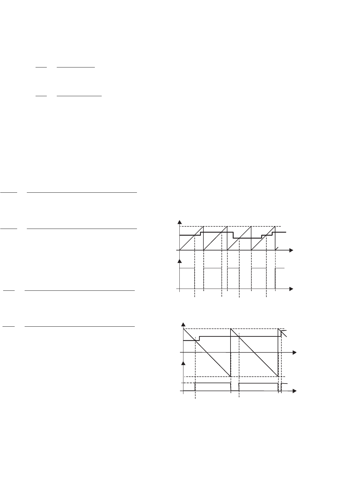
carrier waveform r(t), to obtain the switching variable δ(t )
(Fig. 34.6a). This function controls the power switch, turning
it on at the beginning of the period and turning it off when
the ramp exceeds the u
c
(t) voltage. In Fig. 34.6b the opposite
occurs (turn-off at the end of the period, turn-on when the
u
c
(t) voltage exceeds the ramp).
Considering r(t ) as represented in Fig. 34.6a (r(t ) =
u
cmax
t/T), δ
k
is obtained equating r(t) = u
c
giving δ
k
=
u
c
(t)/u
cmax
or δ
k
/u
c
(t) = G
M
(G
M
=1/u
cmax
). In Fig. 34.6b,
the switching-on angle α
k
is obtained from r(t) = u
cmax
−
2u
cmax
ωt /π, u
c
(t) = u
cmax
−2u
cmax
α
k
/π, giving α
k
= (π/2)×
(1 −u
c
/u
cmax
) and G
M
= ∂α
k
/∂u
c
=−π/(2u
cmax
).
Since, after turn-off or turn-on, any control action variation
of u
c
(t) will only affect the converter duty cycle in the next
period, a time delay is introduced in the control loop. For sim-
plicity, with small-signal perturbations around the operating
point, this delay is assumed almost constant and equal to its
mean value (T/2). Then, the transfer function of the PWM
(b)
u
cmax
−u
cmax
α
1
π+α
2
2πππ/2
δ(t)
u
c
(t)
ωt
ωt
r(t)
1
0
(a)
u
cmax
δ
1
TT+δ
2
T
T
T
2T 3T 4Tt
r(t) u
c
(t)
2T 3T 4Tt
2T+δ
3
T3T+δ
4
T
1
0
δ(t)
FIGURE 34.6 Waveforms of pulse width modulators showing the vari-
able time delays of the modulator response: (a) r(t) = u
cmax
t/T and
(b) r(t ) = u
cmax
−2u
cmax
ωt /π.

34 Control Methods for Switching Power Converters 943
modulator is
˜
δ(s)
˜u
c
(s)
= G
M
e
−sT/2
=
G
M
e
s(T /2)
=
G
M
1 +s
T
2
+
s
2
2!
T
2
2
+···+
s
j
j!
T
2
2
+···
≈
G
M
1 +s
T
2
(34.48)
The final approximation of Eq. (34.48), valid for ωT /2 <
√
2/2, [7] suggests that the PWM modulator can be considered
as an amplifier with gain G
M
and a dominant pole. Notice
that this pole occurs at a frequency doubling the switching
frequency, and most state-space averaged models are valid
only for frequencies below one-tenth of the switching fre-
quency. Therefore, in most situations this modulator pole can
be neglected, being simply δ(s) = G
M
u
c
(s), as the dominant
pole of Eq. (34.48) stays at least one decade to the left of the
dominant poles of the converter.
34.2.5 Linear Feedback Design Ensuring
Stability
In the application of classical linear feedback control to switch-
ing converters, Bode plots and root locus are, usually, suitable
methods to assess system performance and stability. General
rules for the design of the compensated open-loop transfer
function are as follows:
(i) The low-frequency gain should be high enough to
minimize output steady-state errors;
(ii) The frequency of 0 dB gain (unity gain), ω
0dB
, should
be placed close to the maximum allowed by the mod-
eling approximations (λ
max
T 1), to allow fast
response to transients. In practice, this frequency
should be almost an order of magnitude lower than
the switching frequency;
(iii) To ensure stability, the phase margin, defined as
the additional phase shift needed to render the sys-
tem unstable without gain changes (or the difference
between the open-loop system phase at ω
0dB
and
−180
◦
), must be positive and in general greater than
30
◦
(45
◦
−70
◦
is desirable). In the root locus, no poles
should enter the right-half of the complex plane;
(iv) To increase stability, the gain should be less than
−30 dB at the frequency where the phase reaches
−180
◦
(gain margin greater than 30 dB).
Transient behavior and stability margins are related: the
obtained damping factor is generally 0.01 times the phase
margin (in degrees), and overshoot (in percent) is given
approximately by 75
◦
minus the phase margin. The product
of the rise time (in seconds) and the closed-loop bandwidth
(in rad/s) is close to 2.8.
To guarantee gain and phase margins, the following series
compensation transfer functions (usually implemented with
operational amplifiers) are often used [8]:
34.2.5.1 Types of Compensation
Lag or lead compensation
Lag compensation should be used in converters with good sta-
bility margin but poor steady-state accuracy. If the frequencies
1/T
p
and 1/T
z
of Eq. (34.49) with 1/T
p
< 1/T
z
are chosen well
below the unity gain frequency, lag–lead compensation low-
ers the loop gain at high frequency but maintains the phase
unchanged for ω 1/T
z
. Then, the dc gain can be increased to
reduce the steady-state error without significantly decreasing
the phase margin.
C
LL
(s) = k
LL
1 +sT
z
1 +sT
p
= k
LL
T
z
T
p
s +1/T
z
s +1/T
p
(34.49)
Lead compensation can be used in converters with good
steady-state accuracy but poor stability margin. If the fre-
quencies 1/T
p
and 1/T
z
of Eq. (34.49) with 1/T
p
> 1/T
z
are
chosen below the unity gain frequency, lead–lag compensa-
tion increases the phase margin without significantly affecting
the steady-state error. The T
p
and T
z
values are chosen to
increase the phase margin, fastening the transient response
and increasing the bandwidth.
Proportional–Integral compensation
Proportional–integral (PI) compensators (34.50) are used to
guarantee null steady-state error with acceptable rise times.
The PI compensators are a particular case of lag–lead com-
pensators, therefore suitable for converters with good stability
margin but poor steady-state accuracy.
C
PI
(s) =
1 +sT
z
sT
p
=
T
z
T
p
+
1
sT
p
= K
p
+
K
i
s
= K
p
1 +
K
i
K
p
s
= K
p
1 +
1
sT
z
=
1 +sT
z
sT
z
/K
p
(34.50)
Proportional–Integral plus high-frequency pole
compensation
This integral plus zero-pole compensation (34.51) combines
the advantages of a PI with lead or lag compensation. It
can be used in converters with good stability margin but
poor steady-state accuracy. If the frequencies 1/T
M
and 1/T
z
(1/T
z
< 1/T
M
) are carefully chosen, compensation lowers the
loop gain at high frequency, while only slightly lowering the
phase to achieve the desired phase margin.
C
ILD
(s) =
1 +sT
z
sT
p
(
1 +sT
M
)
=
T
z
T
p
T
M
s +1/T
z
s
(
s +1/T
M
)
= W
cp
s +ω
z
s
(
s +ω
M
)
(34.51)

944 J. F. Silva and S. F. Pinto
Proportional–Integral derivative (PID), plus high-frequency
poles
The PID notch filter type (34.52) scheme is used in convert-
ers with two lightly damped complex poles, to increase the
response speed, while ensuring zero steady-state error. In most
switching converters, the two complex zeros are selected to
have a damping factor greater than the converter complex
poles and slightly smaller oscillating frequency. The high-
frequency pole is placed to achieve the needed phase margin
[9]. The design is correct if the complex pole loci, heading to
the complex zeros in the system root locus, never enter the
right half-plane.
C
PIDnf
(s) = T
cp
s
2
+2ξ
cp
ω
0cp
s +ω
2
0cp
s
1 +s/ω
p1
=
T
cp
s
1 +s/ω
p1
+
2T
cp
ξ
cp
ω
0cp
1 +s/ω
p1
+
T
cp
ω
2
0cp
s
1 +s/ω
p1
=
T
cp
s
1 +s/ω
p1
+
T
cp
ω
2
0pc
1 +2sξ
cp
/ω
0cp
s
1 +s/ω
p1
(34.52)
For systems with a high-frequency zero placed at least one
decade above the two lightly damped complex poles, the com-
pensator (34.53), with ω
z1
≈ ω
z2
<ω
p
, can be used. Usually,
the two real zeros present frequencies slightly lower than the
frequency of the converter complex poles. The two high-
frequency poles are placed to obtain the desired phase margin
[9]. The obtained overall performance will often be inferior to
that of the PID type notch filter.
C
PID
(s) = W
cp
(
1 +s/ω
z1
)(
1 +s/ω
z2
)
s
1 +s/ω
p
2
(34.53)
34.2.5.2 Compensator Selection and Design
The procedure to select the compensator and to design its
parameters can be outlined as follows:
1. Compensator selection: In general, since V
DC
per-
turbations exist, null steady-state error guarantee is
needed. High-frequency poles are usually necessary, if
the transfer function shows a −6 dB/octave roll-off due
to high frequency left plane zeros. Therefore, in gen-
eral, two types of compensation schemes with integral
action (34.51 or 34.50), and (34.52 or 34.53) can be
tried. Compensator (34.52) is usually convenient for
systems with lightly damped complex poles;
2. Unity gain frequency ω
0dB
choice:
•
If the selected compensator has no complex zeros,
it is better to be conservative, choosing ω
0dB
well below the frequency of the lightly damped
poles of the converter (or the frequency of the
right half plane zeros if lower). However, because
of the resonant peak of most converter transfer
functions, the phase margin can be obtained at a
frequency near the resonance. If the phase mar-
gin is not enough, the compensator gain must be
lowered;
• If the selected compensator has complex zeros,
ω
0dB
can be chosen slightly above the frequency
of the lightly damped poles;
3. Desired phase margin (φ
M
) specification φ
M
≥ 30
◦
(preferably between 45
◦
and 70
◦
);
4. Compensator zero-pole placement to achieve the
desired phase margin:
• With the integral plus zero-pole compensation
type (34.51), the compensator phase φ
cp
, at the
maximum frequency of unity gain (often ω
0dB
),
equals the phase margin (φ
M
) minus 180
◦
and
minus the converter phase φ
cv
,(φ
cp
= φ
M
−180
◦
−
φ
cv
). The zero-pole position can be obtained cal-
culating the factor f
ct
= tg (π/2 + φ
cp
/2) being
ω
z
= ω
0dB
/f
ct
and ω
M
= ω
0dB
f
ct
.
• With the PID notch filter type (34.52) controller,
the two complex zeros are placed to have a damp-
ing factor equal to two times the damping of
the converter complex poles, and oscillating fre-
quency ω
0cp
30% smaller. The high-frequency pole
ω
p1
is placed to achieve the needed phase margin
(ω
p1
≈ (ω
0cp
·ω
0dB
)
1/2
f
2
ct
with f
ct
= tg(π/2+φ
cp
/2)
and φ
cp
= φ
M
−180
◦
−φ
cv
[5]).
5. Compensator gain calculation (the product of the con-
verter and compensator gains at the ω
0dB
frequency
must be one).
6. Stability margins verification using Bode plots and root
locus.
7. Results evaluation. Restarting the compensator selec-
tion and design, if the attained results are still not good
enough.
34.2.6 Examples: Buck–Boost DC/DC
Converter, Forward DC/DC Converter,
12 Pulse Rectifiers, Buck–Boost DC/DC
Converter in the Discontinuous Mode
(Voltage and Current Mode), Three-phase
PWM Inverters
EXAMPLE 34.4 Feedback design for the buck–boost
dc/dc converter
Consider the converter output voltage v
o
(Fig. 34.1)
to be the controlled output. From Example 34.2 and
Eqs. (34.33) and (34.35), the block diagram of Fig. 34.7 is
obtained. The modulator transfer function is considered
a pure gain (G
M
= 0.1). The magnitude and phase of the
34 Control Methods for Switching Power Converters 945
v
oref
C
P(S)
u
c
Modulator
V
DC
s
2
L
i
C
0
R
0
+
sL
i
+
R
0
(1
_
∆
1
)
2
R
0
∆
1
(1
_
∆
1
)
V
DC
v
0
1
R
0
_
sL
i
∆
1
(1
_
∆
1
)
2
δ
+
+
+
+
+
−
()
FIGURE 34.7 Block diagram of the linearized model of the closed loop buck–boost converter.
Buck-Boost converter, PI plus high frequency pole Buck-Boost converter, PID notch filter
Frequency (rad/s)
10
0
−100
−300
−200
−100
0
100
−50
0
50
Magnitude (dB)Phase (degrees)
−300
−200
−100
0
100
Phase (degrees)
10
1
10
2
10
3
10
4
10
5
Frequency (rad/s)
10
0
−100
−50
0
50
Magnitude (dB)
10
1
10
2
10
3
10
4
10
5
Frequency (rad/s)
(a) (b)
10
0
10
1
10
2
10
3
10
4
10
5
Frequency (rad/s)
3
3
2
2
3
3
1
1
1
2
2
1
10
0
10
1
10
2
10
3
10
4
10
5
FIGURE 34.8 Bode plots for the buck–boost converter. Trace 1 – switching converter magnitude and phase; trace 2 – compensator magnitude and
phase; trace 3 – resulting magnitude and phase of the compensated converter: (a) PI plus high-frequency pole compensation with 60
◦
phase margin,
ω
0dB
= 500 rad/s and (b) PID notch filter compensation with 65
◦
phase margin, ω
0dB
= 1000 rad/s.
open-loop transfer function v
o
/u
c
(Fig. 34.8a trace 1),
shows a resonant peak due to the two lightly damped
complex poles and the associated −12 dB/octave roll-
off. The right half-plane zero changes the roll-off to
−6 dB/octave and adds −90
◦
to the converter phase
(nonminimum-phase converter).
Compensator selection.AsV
DC
perturbations exist null
steady-state error guarantee is needed. High-frequency
poles are needed given the −6 dB/octave final slope
of the transfer function. Therefore, two compensation
schemes (34.51 and 34.52) with integral action are tried
here. The buck–boost converter controlled with integral
plus zero-pole compensation presents, in closed-loop,
two complex poles closer to the imaginary axes than
in open-loop. These poles should not dominate the con-
verter dynamics. Instead, the real pole resulting from the
open-loop pole placed at the origin should be almost
the dominant one, thus slightly lowering the calcu-
lated compensator gain. If the ω
0dB
frequency is chosen
too low, the integral plus zero-pole compensation turns
into a pure integral compensator (ω
z
= ω
M
= ω
0dB
).
However, the obtained gains are too low, leading to very
slow transient responses.
Results showing the transient responses to v
oref
and
V
DC
step changes, using the selected compensators and
converter Bode plots (Fig. 34.8), are shown (Fig. 34.9).
The compensated real converter transient behavior
occurs in the buck and in the boost regions. Notice the
nonminimum-phase behavior of the converter (mainly
in Fig. 34.9b), the superior performance of the PID
notch filter compensator and the unacceptable behav-
ior of the PI with high-frequency pole. Care should be
taken with load changes, when using this compensator,
since instability can easily occur.
The compensator critical values, obtained with the
root-locus studies, are W
cpcrit
= 700 s
−1
for the integral
plus zero-pole compensator, T
cpcrit
= 0.0012 s for the
PID notch filter, and W
Icpcrit
= 18 s
−1
for the integral
compensation derived from the integral plus zero-pole
compensator (ω
z
= ω
M
). This confirms the Bode-plot
design and allows stability estimation with changing
loads and power supply.

946 J. F. Silva and S. F. Pinto
0 0.005 0.01 0.015 0.02 0.025 0.03 0.035 0.04
t [s]
0 0.005 0.01 0.015 0.02 0.025 0.03 0.035 0.04
t [s]
0 0.005 0.01 0.015 0.02 0.025 0.03 0.035 0.04
t [s]
0 0.005 0.01 0.015 0.02 0.025 0.03 0.035 0.04
t [s]
(a) (b)
0
20
40
60
0
10
20
30
2}10*(voref-vo) [V], 1}iL[A]
0
20
40
60
2}10*(voref-vo) [V], 1}iL[A]
1}voref, 2}vo [V]
0
10
20
30
1}voref, 2}vo [V]
FIGURE 34.9 Transient responses of the compensated buck–boost converter. At t = 0.005 s, v
oref
step from 23 to 26 V. At t = 0.02 s, V
DC
step
from 26 to 23 V. Top graphs: step reference v
oref
and output voltage v
o
. Bottom graphs: trace starting at 20 is i
L
current; trace starting at zero is
10 ×(v
oref
−v
o
): (a) PI plus high-frequency pole compensation with 60
◦
phase margin and ω
0dB
= 500 rad/s and (b) PID notch filter compensation
with 64
◦
phase margin and ω
0dB
= 1000 rad/s.
EXAMPLE 34.5 Feedback design for the forward
dc/dc converter
Consider the output voltage v
o
of the forward converter
(Fig. 34.4a) to be the controlled output. From Example
34.3 and Eqs. (34.45) and (34.47), the block diagram of
Fig. 34.10 is obtained. As in Example 34.4, the mod-
ulator transfer function is considered as a pure gain
(G
M
= 0.1). The magnitude and phase of the open-loop
transfer function v
o
/u
c
(Fig. 34.11a, trace 1), shows an
open-loop stable system. Since integral action is needed
to have some disturbance rejection of the voltage source
V
DC
, the compensation schemes used in Example 34.4,
obtained using the same procedure (Fig. 34.11), were
also tested.
Results, showing the transient responses to v
oref
and
V
DC
step changes, are shown (Fig. 34.12). Both com-
pensators (34.51) and (34.52) are easier to design than
the ones for the buck–boost converter, and both have
acceptable performances. Moreover, the PID notch filter
presents a much faster response.
Alternatively, a PID feedback controller such as
Eq. (34.53) can be easily hand-adjusted, starting with
the proportional, integral, and derivative gains all set to
zero. In the first step, the proportional gain is increased
until the output presents an oscillatory response with
nearly 50% overshoot. Next, the derivative gain is slowly
increased until the overshoot is eliminated. Finally, the
integral gain is increased to eliminate the steady-state
error as quickly as possible.
E
XAMPLE 34.6 Feedback design for phase controlled
rectifiers in the continuous mode
Phase controlled, p pulse (p > 1), thyristor recti-
fiers (Fig. 34.13a), operating in the continuous mode,
present an output voltage with p identical segments
within the mains period T . Given this cyclic waveform,
the A, B, C, and D matrices for all these p inter-
vals can be written with the same form, inspite of the
topological variation. Hence, the state-space averaged
model is obtained simply by averaging all the variables
within the period T/p. Assuming small variations, the
mean value of the rectifier output voltage U
DC
can be
written [10]:
U
DC
= U
p
p
π
sin
π
p
cos α (34.54)
where α is the triggering angle of the thyristors, and U
p
the maximum peak value of the rectifier output voltage,
determined by the rectifier topology and the ac sup-
ply voltage. The α value can be obtained (α = (π/2) ×
(1−u
c
/u
cmax
)) using the modulator of Fig. 34.6b, where
ω = 2π/T is the mains frequency. From Eq. (34.54),
the incremental gain K
R
of the modulator plus rectifier
yields:
K
R
=
∂U
DC
∂u
c
= U
p
p
2u
cmax
sin
π
p
cos
πu
c
2u
cmax
(34.55)
For a given rectifier, this gain depends on u
c
, and
should be calculated for a certain quiescent point. How-
ever, for feedback design purposes, keeping in mind that
the rectifier could be required to be stable in all operating