Power electronic handbook
Подождите немного. Документ загружается.

72 S. Abedinpour and K. Shenai
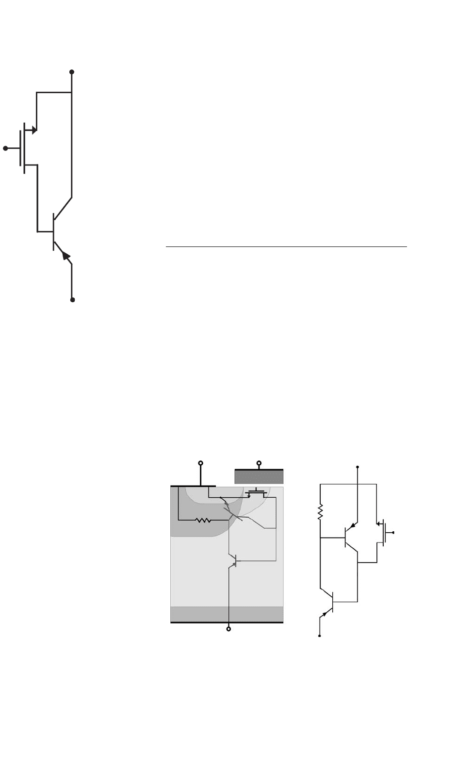
C
BJT
E
G
MOSFET
FIGURE 5.1 Hybrid Darlington configuration of MOSFET and BJT.
can be used for specific applications. The IGBTs are replacing
MOSFETs in high-voltage applications with lower conduc-
tion losses. They have on-state voltage and current density
comparable to a power BJT with higher switching frequency.
Although they exhibit fast turn-on, their turn-off is slower than
a MOSFET because of current fall time. The IGBTs have con-
siderably less silicon area than similar rated power MOSFETs.
Therefore by replacing power MOSFETs with IGBTs, the effi-
ciency is improved and cost is reduced. IGBT is also known
as conductivity modulated FET (COMFET), insulated gate
transistor (IGT), and bipolar-mode MOSFET.
As soft switching topologies offer numerous advantages over
the hard switching topologies, their use is increasing in the
industry. By the use of soft-switching techniques, IGBTs can
operate at frequencies up to hundreds of kilohertz. The IGBTs
behave differently under soft switching condition as opposed
to hard switching conditions. Therefore, the device tradeoffs
involved in soft switching circuits are different than those
in hard switching case. Application of IGBTs in high power
converters subjects them to high-transient electrical stress
such as short circuit and turn-off under clamped inductive
load and therefore robustness of IGBTs under stress condi-
tions is an important requirement. Traditionally, there has
been limited interaction between device manufacturers and
power electronic circuit designers. Therefore, shortcomings of
device reliability are observed only after the devices are used
in actual circuits. This significantly slows down the process
of power electronic system optimization. The development
time can be significantly reduced if all issues of device per-
formance and reliability are taken into consideration at the
design stage. As high stress conditions are quite frequent in
circuit applications, it is extremely cost efficient and perti-
nent to model the IGBT performance under these conditions.
However, development of the model can follow only after the
physics of device operation under stress conditions imposed
by the circuit is properly understood. Physically based process
and device simulations are a quick and cheap way of optimiz-
ing the IGBT. The emergence of mixed mode circuit simulators
in which semiconductor carrier dynamics is optimized within
the constraints of circuit level switching is a key design tool
for this task.
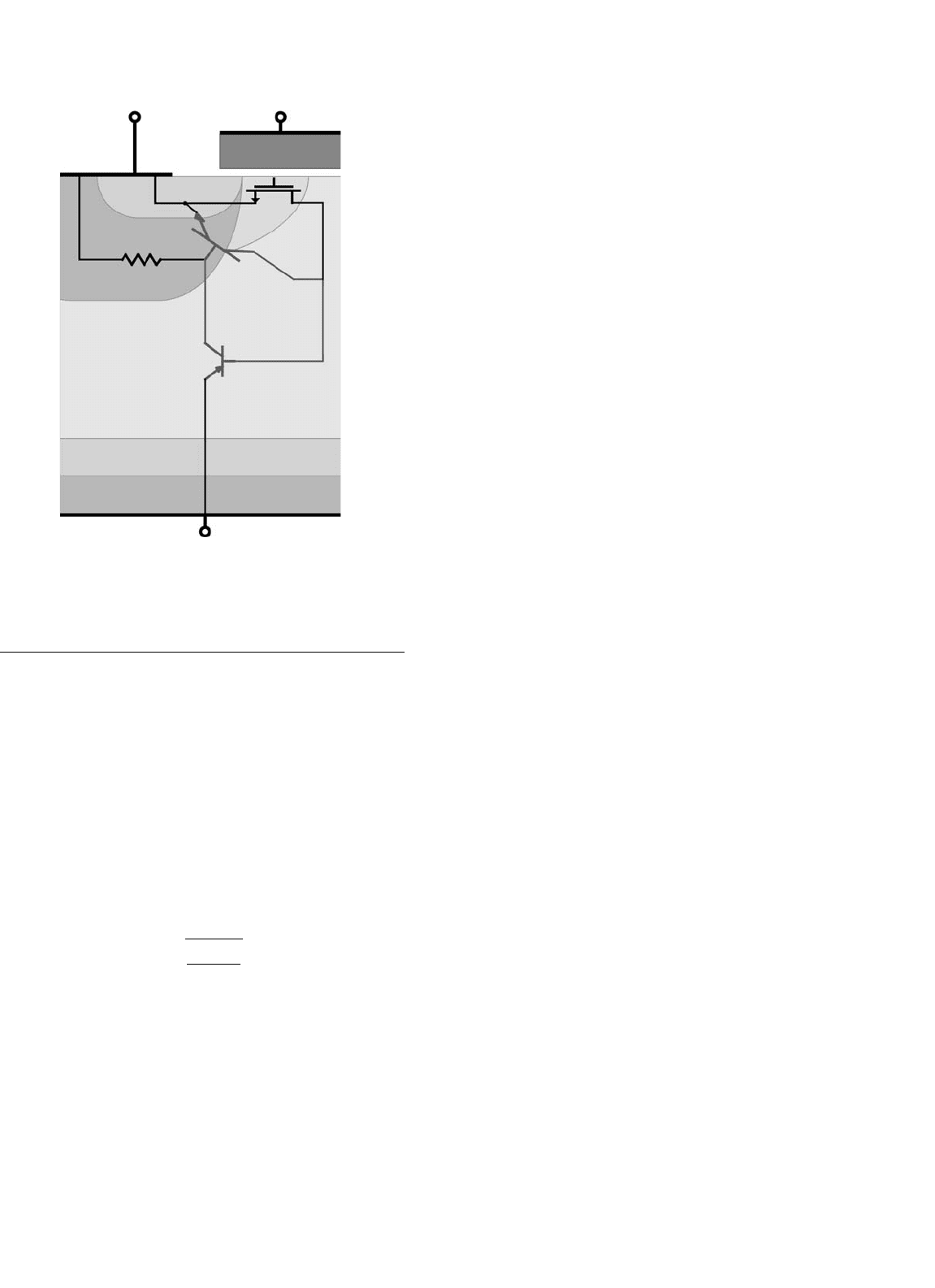
5.2 Basic Structure and Operation
The vertical cross section of a half cell of one of the parallel cells
of an n-channel IGBT shown in Fig. 5.2 is similar to that of a
double diffused power MOSFET (DMOS) except for a p
+
layer
at the bottom. This layer forms the IGBT collector and a pn
junction with n
−
drift region, where conductivity modulation
occurs by injecting minority carriers into the drain drift region
of the vertical MOSFET. Therefore, the current density is much
greater than a power MOSFET and the forward voltage drop
is reduced. The p
+
substrate, n
−
drift layer, and p
+
emitter
constitute a BJT with a wide base region and hence small cur-
rent gain. The device operation can be explained by a BJT with
its base current controlled by the voltage applied to the MOS
gate. For simplicity, it is assumed that the emitter terminal is
connected to the ground potential. By applying a negative volt-
age to the collector, the pn junction between the p
+
substrate
C
PNP
N-MOSFET
G
NPN
E
Gate
Emitter
Collector
n
−
drift
p
+
substrate
p
+
n
+
p-base
(a)
(b)
FIGURE 5.2 IGBT: (a) half-cell vertical cross section and (b) equivalent
circuit model.
5 Insulated Gate Bipolar Transistor 73
and the n
−
drift region is reverse biased which prevents any
current flow and the device is in its reverse blocking state. If
the gate terminal is kept at ground potential but a positive
potential is applied to the collector, the pn junction between
the p-base and n
−
drift region is reverse biased. This prevents
any current flow and the device is in its forward blocking
state until the open base breakdown of the pnp transistor is
reached.
When a positive potential is applied to the gate and exceeds
the threshold voltage required to invert the MOS region under
the gate an n channel is formed, which provides a path for
electrons to flow into the n
−
drift region. The pn junction
between the p
+
substrate and n
−
drift region is forward biased
and holes are injected into the drift region. The electrons in
the drift region recombine with these holes to maintain space
charge neutrality and the remaining holes are collected at the
emitter, causing a vertical current flow between the emitter
and collector. For small values of collector potential and a gate
voltage larger than the threshold voltage the on-state char-
acteristics can be defined by a wide base power BJT. As the
current density increases, the injected carrier density exceeds
the low doping of the base region and becomes much larger
than the background doping. This conductivity modulation
decreases the resistance of the drift region, and therefore IGBT
has a much greater current density than a power MOSFET
with reduced forward voltage drop. The base–collector junc-
tion of the pnp BJT cannot be forward biased, and therefore
this transistor will not operate in saturation. But when the
potential drop across the inversion layer becomes comparable
to the difference between the gate voltage and threshold volt-
age, channel pinch-off occurs. The pinch-off limits the electron
current and as a result the holes injected from the p
+
layer.
Therefore, base current saturation causes the collector current
to saturate.
COLLECTOR CURRENT (A)
1
2
3
462
0
0
GATE VOLTAGE (V)
COLLECTOR CURRENT (A)
0
010864212
1
2
3
4
5
6
7
V
GE
= 10 V
9 V
8 V
7 V
6 V
COLLECTOR VOLTAGE (V)
FIGURE 5.3 IGBT: (a) forward characteristics and (b) transfer characteristics.
Typical forward characteristics of an IGBT as a function of
gate potential and IGBT transfer characteristics are shown in
Fig. 5.3. The transfer characteristics of IGBT and MOSFET
are similar. The IGBT is in the off-state if the gate–emitter
potential is below the threshold voltage. For gate voltages
greater than the threshold voltage, the transfer curve is linear
over most of the drain current range. Gate-oxide breakdown
and the maximum IGBT drain current limit the maximum
gate–emitter voltage.
To turn-off the IGBT, gate is shorted to the emitter to
remove the MOS channel and the base current of the pnp
transistor. The collector current is suddenly reduced because
the electron current from channel is removed. Then the excess
carriers in the n
−
drift region decay by electron–hole recombi-
nation, which causes a gradual collector current decay. In order
to keep the on-state voltage drop low, the excess carrier lifetime
must be kept large. Therefore, similar to the other minority
carrier devices there is a tradeoff between on-state losses and
faster turn-off switching times. In the punch-through (PT)
IGBT structure of Fig. 5.4 the switching time is reduced by
use of a heavily doped n buffer layer in the drift region near
the collector. Because of much higher doping density in the
buffer layer, the injection efficiency of the collector junction
and the minority carrier lifetime in the base region is reduced.
The smaller excess carrier lifetime in the buffer layer sinks the
excess holes. This speeds up the removal of holes from the
drift region and therefore decreases the turn-off time. Non-
punch-through (NPT) IGBTs have higher carrier lifetimes and
low doped shallow collector region, which affect their electrical
characteristics. In order to prevent punch through, NPT IGBTs
have a thicker drift region, which results in a higher base transit
time. Therefore in NPT structure carrier lifetime is kept more
than that of a PT structure, which causes conductivity modu-
lation of the drift region and reduces the on-state voltage drop.
74 S. Abedinpour and K. Shenai
Collector
p
+
substrate
n buffer
n
−
drift
p
+
n
+
p-base
GateEmitter
FIGURE 5.4 Punch-through (PT) IGBT structure.
5.3 Static Characteristics
In the IGBT structure of Fig. 5.2, if a negative voltage is applied
to the collector, the junction between the p
+
substrate and
n
−
drift region becomes reverse biased. The drift region is
lightly doped and the depletion layer extends principally into
the drift region. An open base transistor exists between the
p
+
substrate, n
−
drift region, and the p-base region. The dop-
ing concentration (N
D
) and thickness of the n
−
drift region
(W
D
) are designed to avoid the breakdown of this structure.
The width of the drift region affects the forward voltage drop
and therefore, should be optimized for a desired breakdown
voltage. The thickness of the drift region (W
D
) is chosen equal
to the sum of one diffusion length (L
p
) and the width of the
depletion layer at maximum applied voltage (V
max
).
W
D
=
2ε
s
V
max
qN
D
+L
P
(5.1)
When the gate is shorted to the emitter, no channel exists
under the gate. Therefore, if a positive voltage is applied to the
collector the junction between the p-base and n
−
drift region is
reverse biased and only a small leakage current flows through
IGBT. Similar to a MOSFET the depletion layer extends into
the p-base and n
−
drift region. The p-base doping concen-
tration, which also controls the threshold voltage is chosen to
avoid punch through of the p-base to n
+
emitter. In ac cir-
cuit applications, which require identical forward and reverse
blocking capability the drift region thickness of the symmet-
rical IGBT shown in Fig. 5.2 is designed by use of Eq. (5.1)
to avoid reach through of the depletion layer to the junction
between the p
+
collector and the n
−
drift region. When IGBT
is used in dc circuits, which do not require reverse blocking
capability a highly doped n buffer layer is added to the drift
region near the collector junction to form a PT IGBT. In this
structure, the depletion layer occupies the entire drift region
and the n buffer layer prevents reach through of the depletion
layer to the p
+
collector layer. Therefore the required thick-
ness of the drift region is reduced, which reduces the on-state
losses. But the highly doped n buffer layer and p
+
collector
layer degrade the reverse blocking capability to a very low
value. Therefore on-state characteristics of a PT IGBT can be
optimized for a required forward blocking capability while the
reverse blocking capability is neglected.
When a positive voltage is applied to the gate of an IGBT,
an MOS channel is formed between the n
+
emitter and the
n
−
drift region. Therefore a base current is provided for the
parasitic pnp BJT. By applying a positive voltage between
the collector and emitter electrodes of an n type IGBT, minor-
ity carriers (holes) are injected into the drift region. The
injected minority carriers reduce the resistivity of the drift
region and reduce the on-state voltage drop resulting in a
much higher current density compared to a power MOSFET.
If the shorting resistance between the base and emitter of the
npn transistor is small, the n
+
emitter p-base junction does not
become forward biased and therefore the parasitic npn transis-
tor is not active and can be deleted from the equivalent IGBT
circuit. The analysis of the forward conduction characteristics
of an IGBT is possible by the use of two equivalent circuit
approaches. The model based on a PiN rectifier in series with
a MOSFET, shown in Fig. 5.5b is easy to analyze and gives
a reasonable understanding of the IGBT operation. But this
model does not account for the hole current component flow-
ing into the p-base region. The junction between the p-base
and the n
−
drift region is reverse biased. This requires that
the free carrier density be zero at this junction, and therefore
results in a different boundary condition for IGBT compared
to those for PiN rectifier. The IGBT conductivity modulation
in the drift region is identical to the PiN rectifier near the col-
lector junction, but it is less than a PiN rectifier near the p-base
junction. Therefore, the model based on a bipolar pnp tran-
sistor driven by a MOSFET in Fig. 5.5a gives a more complete
description of the conduction characteristics.
Analyzing the IGBT operation by the use of these models
shows that IGBT has one diode drop due to the parasitic diode.
Below the diode knee voltage, there is negligible current flow
due to the lack of minority carrier injection from the collector.
Also by increasing the applied voltage between the gate and
emitter, the base of the internal bipolar transistor is supplied by
more base current, which results in an increase in the collector
5 Insulated Gate Bipolar Transistor 75
PiN DIODE
PNP
N-MOSFET
C
C
G
G
E
E
N-MOSFET
(a) (b)
FIGURE 5.5 IGBT equivalent circuits: (a) BJT/MOSFET and (b) PiN/
MOSFET.
current. The IGBT current shows saturation due to the pinch-
off of the MOS channel. This limits the input base current of
the bipolar transistor. The MOS channel of the IGBT reverse
biases the collector–base junction and forces the bipolar pnp
transistor to operate in its active region. The drift region is in
high-level injection at the required current densities and wider
n
−
drift region results in higher breakdown voltage.
Because of the very low gain of the pnp BJT, the driver MOS-
FET in the equivalent circuit of the IGBT carries a major por-
tion of the total collector current. Therefore, the IGBT on-state
voltage drop as is shown in Fig. 5.6 consists of voltage drop
across the collector junction, drift region, and MOSFET por-
tion. The low value of the drift region conductivity modulation
near the p-base junction causes a substantial drop across the
junction field effect transistor (JFET) resistance of the MOS-
FET (V
JFET
) in addition to the voltage drop across the channel
resistance (V
ch
) and the accumulation layer resistance (V
acc
).
V
CE(on)
= V
p
+
n
+V
drift
+V
MOSFET
(5.2)
V
MOSFET
= V
ch
+V
JFET
+V
acc
(5.3)
When the lifetime in the n
−
drift region is large, the gain
of the pnp bipolar transistor is high and its collector current
is much larger than the MOSFET current and therefore, the
voltage drop across the MOSFET component of IGBT is a
small fraction of the total voltage drop. When lifetime control
techniques are used to increase the switching speed, the current
gain of the bipolar transistor is reduced and a greater portion
of the current flows through the MOSFET channel and there-
fore the voltage drop across the MOSFET increases. In order
to decrease the resistance of the MOSFET current path, trench
IGBTs can be used as shown in Fig. 5.7. Extending the trench
gate below the p-base and n
−
drift region junction forms
a channel between the n
+
emitter and the n
−
drift region.
This eliminates the JFET and accumulation layer resistance
Collector
p
+
substrate
n
−
drift
parasitic
thyristor
p
+
n
+
p-base
Emitter Gate
V
ch
V
JFET
V
p
+
n
V
drift
V
acc
−
−
−
−
−
+
+
+
+
+
FIGURE 5.6 Components of on-state voltage drop within the IGBT
structure.
Collector
p
+
substrate
n
−
drift
n buffer
p
+
n
+
p-base
Emitter
Gate
FIGURE 5.7 Trench IGBT structure.
76 S. Abedinpour and K. Shenai
and therefore reduces the voltage drop across the MOSFET
component of IGBT, which results in a superior conduction
characteristics. By the use of trench structure, the IGBT cell
density and latching current density are also improved.
5.4 Dynamic Switching Characteristics
5.4.1 Turn-on Characteristics
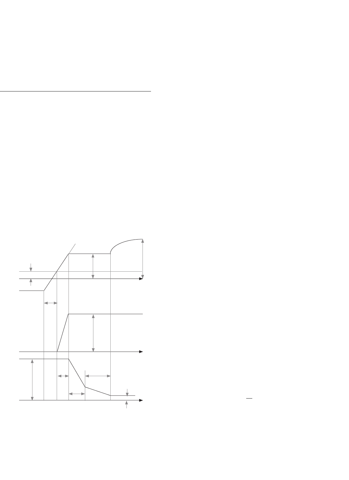
The switching waveforms of an IGBT in a clamped inductive
circuit are shown in Fig. 5.8. The L/R time constant of the
inductive load is assumed to be large compared to the switch-
ing frequency and therefore, can be considered as a constant
current source I
on
. The IGBT turn-on switching performance
is dominated by its MOS structure. During t
d(on)
, the gate cur-
rent charges the constant input capacitance with a constant
slope until the gate–emitter voltage reaches the threshold volt-
age V
GE(th)
of the device. During t
ri
, load current is transferred
from the diode into the device and increases to its steady-state
value.
The gate voltage rise time and IGBT transconductance
determine the current slope and results as t
ri
. When the
gate–emitter voltage reaches V
GE(Ion)
, which will support the
steady-state collector current, collector–emitter voltage starts
to decrease. After this there are two distinct intervals, during
V
GE(th)
V
GG
+
t
t
t
I
on
t
d(on)
t
ri
V
cc
v
CE
(t)
i
C
(t)
v
GE
(t)
t
fv1
t
fv2
V
CE(on)
V
GE(Ion)
FIGURE 5.8 IGBT turn-on waveforms in a clamped inductive load
circuit.
IGBT turn-on. In the first interval, the collector to emitter
voltage drops rapidly as the gate–drain capacitance C
gd
of the
MOSFET portion of IGBT discharges. At low collector–emitter
voltage C
gd
increases. A finite time is required for high-level
injection conditions to set in the drift region. The pnp transis-
tor portion of IGBT has a slower transition to its on-state than
the MOSFET. The gate voltage starts rising again only after
the transistor comes out of its saturation region into the linear
region, when complete conductivity modulation occurs and
the collector–emitter voltage reaches its final on-state value.
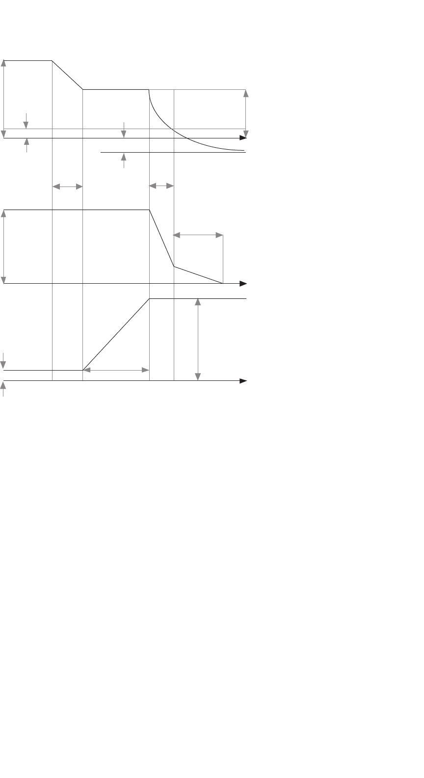
5.4.2 Turn-off Characteristics
Turn-off begins by removing the gate–emitter voltage. Volt-
age and current remain constant until the gate voltage reaches
V
GE(Ion)
, required to maintain the collector steady-state cur-
rent as shown in Fig. 5.9. After this delay time (t
d(off )
) the
collector voltage rises, while the current is held constant. The
gate resistance determines the rate of collector voltage rise.
As the MOS channel turns off, collector current decreases
sharply during t
fi1
. The MOSFET portion of IGBT deter-
mines the turn-off delay time t
d(off )
and the voltage rise
time t
rv
. When the collector voltage reaches the bus voltage,
the freewheeling diode starts to conduct.
However the excess stored charge in the n
−
drift region
during on-state conduction, must be removed for the device
to turn-off. The high minority carrier concentration stored
in the n
−
drift region supports the collector current after the
MOS channel is turned off. Recombination of the minority
carriers in the wide base region gradually decreases the col-
lector current and results in a current tail. Since there is no
access to the base of the pnp transistor, the excess minority
carriers cannot be removed by reverse biasing the gate. The
t
fi2
interval is long because the excess carrier lifetime in this
region is normally kept high to reduce the on-state voltage
drop. Since the collector–emitter voltage has reached the bus
voltage in this interval, a significant power loss occurs which
increases with frequency. Therefore, the current tail limits the
IGBT operating frequency and there is a tradeoff between the
on-state losses and faster switching times. For an on-state cur-
rent of I
on
, the magnitude of the current tail, and the time
required for the collector current to decrease to 10% of its
on-state value, turn-off (t
off
) time, are approximated as:
I
c
(t) = α
pnp
I
on
e
−t/τ
HL
(5.4)
t
off
= τ
HL
ln(10α
pnp
) (5.5)
where
α
pnp
= sec h
l
L
a
(5.6)
is the gain of the bipolar pnp transistor, l is the undepleted
base width, and L
a
is the ambipolar diffusion length and it
5 Insulated Gate Bipolar Transistor 77
V
GE(th)
V
GG
+
t
t
t
I
on
t
d(off)
t
rv
V
cc
v
CE
(t)
i
C
(t)
v
GE
(t)
V
CE(on)
V
GG
−
t
fi2
t
fi1
V
GE(Ion)
FIGURE 5.9 Switching waveforms during IGBT clamped inductive load turn-off.
is assumed that the high level lifetime (τ
HL
) is independent
of the minority carrier injection during the collector current
decay.
Lifetime-control techniques are used to reduce the life-
time (τ
HL
) and the gain of the bipolar transistor (α
pnp
). As a
result, the magnitude of the current tail and t
off
decrease. But
the conductivity modulation decreases, which increases the
on-state voltage drop in the drift region. Therefore, higher
speed IGBTs have a lower current rating. Thermal diffusion
of impurities such as gold and platinum introduces recombi-
nation centers, which reduce the lifetime. The device can also
be irradiated with high-energy electrons to generate recom-
bination centers. Electron irradiation introduces a uniform
distribution of defects, which results in reduction of lifetime
in the entire wafer and affects the conduction properties of the
device. Another method of lifetime control is proton implan-
tation, which can place defects at a specific depth. Therefore,
it is possible to have a localized control of lifetime to improve
the tradeoff between the on-state voltage and switching speed
of the device. The turn-off loss can be minimized by curtailing
the current tail as a result of speeding up the recombination
process in the portion of the drift region, which is not swept
by the reverse bias.
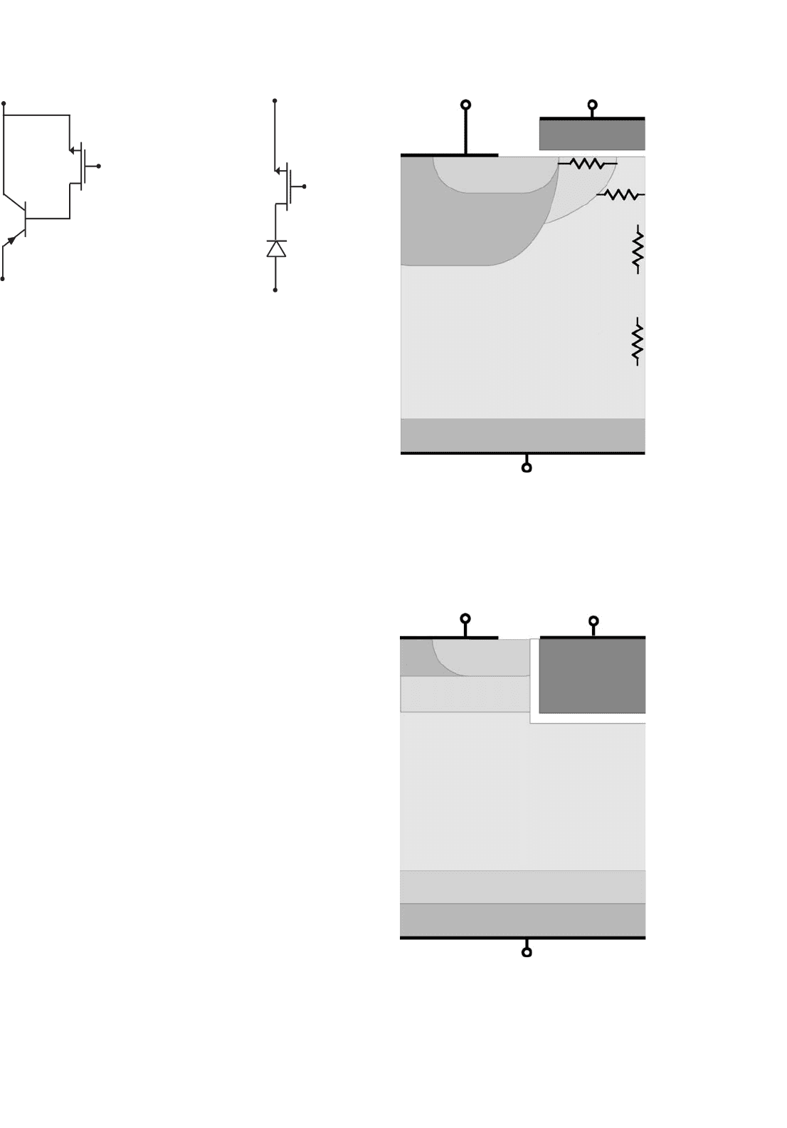
5.4.3 Latch-up of Parasitic Thyristor
A portion of minority carriers injected into the drift region
from the collector of an IGBT flows directly to the emitter
terminal. The negative charge of electrons in the inversion
layer attracts the majority of holes and generates the lateral
component of hole current through the p-type body layer as
shown in Fig. 5.10. This lateral current flow develops a volt-
age drop across the spreading resistance of the p-base region,
which forward biases the base–emitter junction of the npn
parasitic BJT. By designing a small spreading resistance, the
voltage drop is lower than the built-in potential and therefore
the parasitic thyristor between the p
+
collector region, n
−
drift
region, p-base region, and n
+
emitter does not latch-up. Larger
values of on-state current density produce a larger voltage
drop, which causes injection of electrons from the emitter
region into the p-base region and hence turns on the npn
transistor. When this occurs the pnp transistor will turn-on,
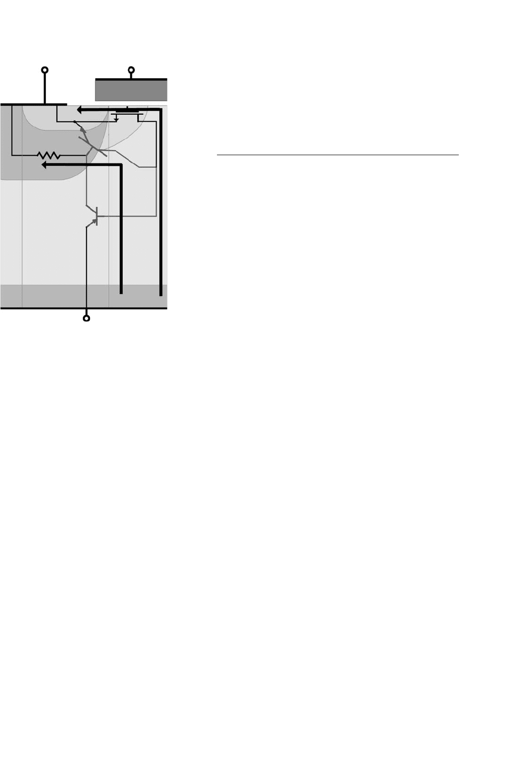
78 S. Abedinpour and K. Shenai
p-base
Emitter
Gate
Collector
p
+
substrate
n
−
drift
parasitic
thyristor
p
+
n
+
FIGURE 5.10 On-state current flow paths in an IGBT structure.
therefore the parasitic thyristor will latch-up and the gate loses
control over the collector current.
Under dynamic turn-off conditions the magnitude of the
lateral hole current flow increases and latch-up can occur at
lower on-state currents compared to the static condition. The
parasitic thyristor latches up when the sum of the current gains
of the npn and pnp transistors exceeds one. When the gate
voltage is removed from IGBT with a clamped inductive load,
its MOSFET component turns off and reduces the MOSFET
current to zero very rapidly. As a result the drain–source volt-
age rises rapidly and is supported by the junction between the
n
−
drift region and the p-base region. The drift region has a
lower doping and therefore the depletion layer extends more in
the drift region. As a result the current gain of the pnp transis-
tor portion, α
pnp
increases and a greater portion of the injected
holes into the drift region will be collected at the junction of
p-base and n
−
drift regions. Therefore, the magnitude of the
lateral hole current increases, which increases the lateral volt-
age drop. As a result the parasitic thyristor will latch-up even
if the on-state current is less than the static latch-up value.
Reducing the gain of the npn or pnp transistors can pre-
vent the parasitic thyristor latch-up. A reduction in the gain
of the pnp transistor increases the IGBT on-state voltage drop.
Therefore in order to prevent the parasitic thyristor latch-up, it
is better to reduce the gain of the npn transistor component of
IGBT. Reduction of carrier lifetime, use of buffer layer, and use
of deep p
+
diffusion improve the latch-up immunity of IGBT.
But inadequate extent of the p
+
region may fail to prevent the
device from latch-up. Also care should be taken that the p
+
diffusion does not extend into the MOS channel because this
causes an increase in the MOS threshold voltage.
5.5 IGBT Performance Parameters
The IGBTs are characterized by certain performance param-
eters. The manufacturers specify these parameters, which are
described below, in the IGBT data sheet. The important rat-
ings of IGBTs are values, which establish either a minimum
or maximum limiting capability or limiting condition. The
IGBTs cannot be operated beyond the maximum or minimum
rating’s value, which are determined for a specified operating
point and environment condition.
Collector–Emitter blocking voltage (BV
CES
): This parameter
specifies the maximum off-state collector–emitter voltage
when the gate and emitter are shorted. Breakdown is speci-
fied at a specific leakage current and varies with temperature
by a positive temperature coefficient.
Emitter–Collector blocking voltage (BV
ECS
): This parameter
specifies the reverse breakdown of the collector–base junc-
tion of the pnp transistor component of IGBT.
Gate–Emitter voltage (V
GES
): This parameter determines the
maximum allowable gate–emitter voltage, when collector
is shorted to emitter. The thickness and characteristics of
the gate-oxide layer determine this voltage. The gate volt-
age should be limited to a much lower value to limit the
collector current under fault conditions.
Continuous collector current (I
C
): This parameter represents the
value of the dc current required to raise the junction to
its maximum temperature, from a specified case tempera-
ture. This rating is specified at a case temperature of 25
◦
C
and maximum junction temperature of 150
◦
C. Since nor-
mal operating condition cause higher case temperatures, a
plot is given to show the variation of this rating with case
temperature.
Peak collector repetitive current (I
CM
): Under transient con-
ditions, the IGBT can withstand higher peak currents
compared to its maximum continuous current, which is
described by this parameter.
Maximum power dissipation (P
D
): This parameter represents the
power dissipation required to raise the junction tempera-
ture to its maximum value of 150
◦
C, at a case temperature
of 25
◦
C. Normally a plot is provided to show the variation
of this rating with temperature.
Junction temperature (T
j
): Specifies the allowable range of the
IGBT junction temperature during its operation.
Clamped inductive load current (I
LM
): This parameter specifies
the maximum repetitive current that IGBT can turn-off
under a clamped inductive load. During IGBT turn-on, the
reverse recovery current of the freewheeling diode in par-
allel with the inductive load increases the IGBT turn-on
switching loss.
5 Insulated Gate Bipolar Transistor 79
Collector–Emitter leakage current (I
CES
): This parameter deter-
mines the leakage current at the rated voltage and specific
temperature when the gate is shorted to emitter.
Gate–Emitter threshold voltage (V
GE(th)
): This parameter spec-
ifies the gate–emitter voltage range, where the IGBT is
turned on to conduct the collector current. The threshold
voltage has a negative temperature coefficient. Threshold
voltage increases linearly with gate-oxide thickness and as
the square root of the p-base doping concentration. Fixed
surface charge at the oxide–silicon interface and mobile ions
in the oxide shift the threshold voltage.
Collector–Emitter saturation voltage (V
CE(SAT)
): This parameter
specifies the collector–emitter forward voltage drop and is a
function of collector current, gate voltage, and temperature.
Reducing the resistance of the MOSFET channel and JFET
region, and increasing the gain of the pnp bipolar transis-
tor can minimize the on-state voltage drop. The voltage
drop across the MOSFET component of IGBT, which pro-
vides the base current of the pnp transistor is reduced by a
larger channel width, shorter channel length, lower thresh-
old voltage, and wider gate length. Higher minority carrier
lifetime and a thin n-epi region cause high carrier injection
and reduce the voltage drop in the drift region.
Forward transconductance (g
FE
): Forward transconductance is
measured with a small variation on the gate voltage, which
linearly increases the IGBT collector current to its rated cur-
rent at 100
◦
C. The transconductance of an IGBT is reduced
at currents much higher than its thermal handling capabil-
ity. Therefore, unlike the bipolar transistors, the current
handling capability of IGBTs is limited by thermal con-
sideration and not by its gain. At higher temperatures,
the transconductance starts to decrease at lower collec-
tor currents. Therefore, these features of transconductance
protects the IGBT under short circuit operation.
Total gate charge (Q
G
): This parameter helps to design a suit-
able size gate drive circuit and approximately calculate its
losses. Because of the minority carrier behavior of device,
the switching times cannot be approximately calculated by
the use of gate charge value. This parameter varies as a
function of the gate–emitter voltage.
Turn-on delay time (t
d
): It is defined as the time between 10%
of gate voltage and 10% of the final collector current.
Rise time (t
r
): It is the time required for the collector current to
increase to 90% of its final value from 10% of its final value.
Turn-off delay time (t
d(off )
): It is the time between 90% of gate
voltage and 10% of final collector voltage.
Fall time (t
f
): It is the time required for the collector current
to drop from 90% of its initial value to 10% of its initial
value.
Input capacitance (C
ies
): It is the measured gate–emitter capac-
itance when collector is shorted to emitter. The input
capacitance is the sum of the gate–emitter and the miller
capacitance. The gate–emitter capacitance is much larger
than the miller capacitance.
Output capacitance (C
oes
): It is the capacitance between collector
and emitter when gate is shorted to the emitter, which has
the typical pn junction voltage dependency.
Reverse transfer capacitance (C
res
): It is the miller capacitance
between gate and collector, which has a complex voltage
dependency.
Safe operating area (SOA): The safe operating area determines
the current and voltage boundary within which the IGBT
can be operated without destructive failure. At low cur-
rents the maximum IGBT voltage is limited by the open
base transistor breakdown. The parasitic thyristor latch-
up limits the maximum collector current at low voltages.
The IGBTs immune to static latch-up may be vulnerable to
dynamic latch-up. Operation in short circuit and inductive
load switching are conditions that would subject an IGBT
to a combined voltage and current stress. Forward biased
safe operating area (FBSOA) is defined during the turn-on
transient of the inductive load switching when both elec-
tron and hole current flow in the IGBT in the presence of
high voltage across the device. The reverse biased safe oper-
ating area (RBSOA) is defined during the turn-off transient,
where only hole current flows in the IGBT with high voltage
across it.
If the time duration of simultaneous high voltage and high
current is long enough, the IGBT failure will occur because of
thermal breakdown. But if this time duration is short, the tem-
perature rise due to power dissipation will not be enough to
cause thermal breakdown. Under this condition the avalanche
breakdown occurs at voltage levels lower than the breakdown
voltage of the device. Compared to the steady-state forward
blocking condition the much larger charge in the drift region
causes a higher electric field and narrower depletion region at
the p-base and n
−
drift junction. Under RBSOA conditions
there is no electron in the space charge region, and there-
fore there is a larger increase in electric field than the FBSOA
condition.
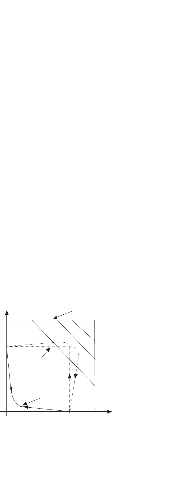
The IGBT SOA is indicated in Fig. 5.11. Under short-
switching times the rectangular SOA shrinks by increase in
DC
10
−4
sec
10
−5
sec
Switch-mode
Zero-voltage/
zero current
switching
v
T
i
T
V
BUS
V
BD
I
o
SOA
FIGURE 5.11 IGBT safe operating area (SOA).
80 S. Abedinpour and K. Shenai
the duration of on-time. Thermal limitation is the reason for
smaller SOA and the lower limit is set by dc operating condi-
tions. The device switching loci under hard switching (dashed
lines) and zero voltage or zero current switching (solid lines)
is also indicated in Fig. 5.11. The excursion is much wider
for switch-mode hard-switching applications than for the soft-
switching case, and therefore a much wider SOA is required for
hard-switching applications. Presently IGBTs are optimized
for hard-switching applications. In soft-switching applications
the conduction losses of IGBT can be optimized at the cost of
smaller SOA. In this case the p-base doping can be adjusted
to result in a much lower threshold voltage and hence for-
ward voltage drop. But in hard-switching applications, the
SOA requirements dominate over forward voltage drop and
switching time. Therefore, the p-base resistance should be
reduced, which causes a higher threshold voltage. As a result,
the channel resistance and forward voltage drop will increase.
5.6 Gate Drive Requirements
The gate drive circuit acts as an interface between the logic sig-
nals of the controller and the gate signals of the IGBT, which
reproduces the commanded switching function at a higher
power level. Non-idealities of the IGBT such as finite volt-
age and current rise and fall times, turn-on delay, voltage and
current overshoots, and parasitic components of the circuit
cause differences between the commanded and real wave-
forms. Gate drive characteristics affect the IGBT non-idealities.
The MOSFET portion of the IGBT drives the base of the pnp
transistor and therefore the turn-on transient and losses is
greatly affected by the gate drive.
Due to lower switching losses, soft-switched power convert-
ers require gate drives with higher power ratings. The IGBT
gate drive must have sufficient peak current capability to pro-
vide the required gate charge for zero current switching and
zero voltage switching. The delay of the input signal to the
gate drive should be small compared to the IGBT switching
period and therefore, the gate drive speed should be designed
properly to be able to use the advantages of faster switching
speeds of the new generation IGBTs.
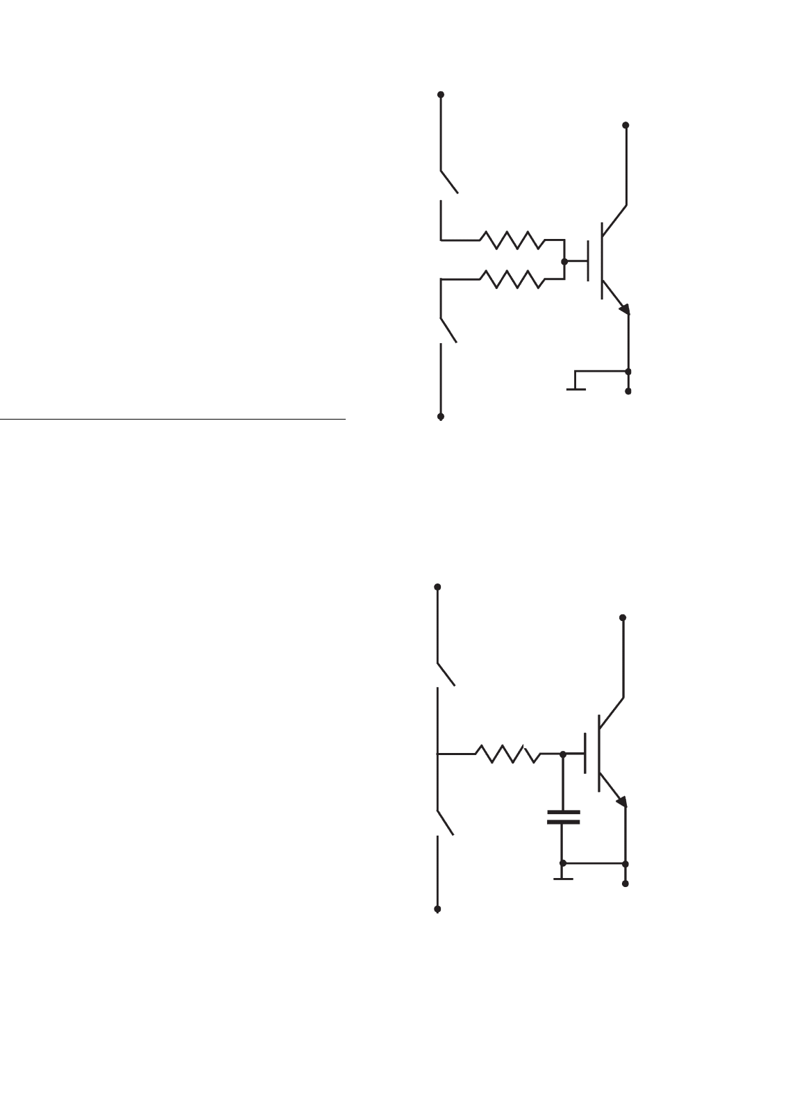
5.6.1 Conventional Gate Drives
The first IGBT gate drives used fixed passive components and
were similar to MOSFET gate drives. Conventional gate drive
circuits use a fixed gate resistance for turn-on and turn-off
as shown in Fig. 5.12. The turn-on gate resistor R
gon
limits
the maximum collector current during turn-on, and the turn-
off gate resistor R
goff
limits the maximum collector–emitter
voltage. In order to decouple the dv
ce
/dt and di
c
/dt control,
an external capacitance C
g
can be used at the gate, which
increases the time constant of the gate circuit and reduces the
di
c
/dt as shown in Fig. 5.13. But C
g
does not affect the dv
ce
/dt
E
V
gg
−
R
goff
R
gon
V
gg
+
C
G
FIGURE 5.12 Gate drive circuit with independent turn-on and turn-off
resistors.
C
E
G
R
g
C
g
V
gg
+
V
gg
−
FIGURE 5.13 External gate capacitor for decoupling dv
ce
/dt and di
c
/dt
during switching transient.
5 Insulated Gate Bipolar Transistor 81
transient, which occurs during the miller plateau region of the
gate voltage.
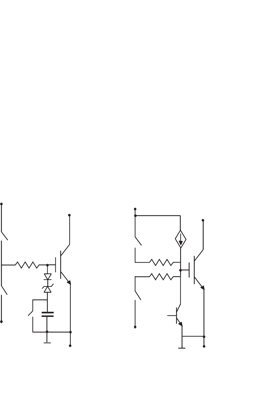
5.6.2 New Gate Drive Circuits
In order to reduce the delay time required for the gate voltage
to increase from V
gg−
to V
ge
(th), the external gate capacitor
can be introduced in the circuit only after V
ge
reaches V
ge
(th)
as is shown in Fig. 5.14, where the collector current rise occurs.
The voltage tail during turn-on transient is not affected by this
method. In order to prevent shoot through caused by acci-
dental turn-on of IGBT due to noise, a negative gate voltage
is required during off-state. Low gate impedance reduces the
effect of noise on gate.
During the first slope of the gate voltage turn-on tran-
sient, the rate of charge supply to the gate determines the
collector current slope. During the miller effect zone of the
turn-on transient the rate of charge supply to the gate deter-
mines the collector voltage slope. Therefore, the slope of the
collector current, which is controlled by the gate resistance,
strongly affects the turn-on power loss. Reduction in switch-
ing power loss requires low gate resistance. But the collector
current slope also determines the amplitude of the conducted
electromagnetic interference (EMI) during turn-on switching
transient. Lower EMI generation requires higher values of gate
resistance. Therefore, in conventional gate drive circuits by
C
E
G
R
g
C
g
V
gg
+
V
gg
−
FIGURE 5.14 A circuit for reducing the turn-on delay.
selecting an optimum value for R
g
, there is a tradeoff between
lower switching losses and lower EMI generation.
But the turn-off switching of IGBT depends on the bipolar
characteristics. Carrier lifetime determines the rate at which
the minority carriers stored in the drift region recombine.
The charge removed from the gate during turn-off has small
influence on minority carrier recombination. The tail current
and di/dt during turn-off, which determine the turn-off losses,
depend mostly on the amount of stored charge and the minor-
ity carriers lifetime. Therefore, the gate drive circuit has a
minor influence on turn-off losses of the IGBT, while it affects
the turn-on switching losses.
The turn-on transient is improved by use of the circuit
shown in Fig. 5.15. The additional current source increases the
gate current during the tail voltage time, and therefore reduces
the turn-on loss. The initial gate current is determined by V
gg
+
and R
gon
, which are chosen to satisfy device electrical spec-
ifications and EMI requirements. After the collector current
reaches its maximum value, the miller effect occurs and the
controlled current source is enabled to increase the gate cur-
rent to increase the rate of collector voltage fall. This reduces
the turn-on switching loss. Turn-off losses can only be reduced
during the miller effect and MOS turn-off portion of the turn-
off transient, by reducing the gate resistance. But this increases
the rate of change of collector voltage, which strongly affects
the IGBT latching current and RBSOA. During the turn-off
C
E
G
R
gon
R
goff
T
1
V
gg
+
V
gg
−
FIGURE 5.15 Schematic circuit of an IGBT gate drive circuit.