Power electronic handbook
Подождите немного. Документ загружается.

92 A. Bryant et al.
in significant carrier multiplication, denoted as a multiplying
factor M on the current components, I
co
and i
G
.
i
A
=
MI
co
+Mα
n
i
G
1 −M(α
n
+α
p
)
(6.1)
In the forward-blocking state, the leakage current I
co
is small,
both α’s are small, and their sum is less than unity. Gate cur-
rent increases the current in both transistors, increasing their
α’s. Collector current in the npn transistor acts as base cur-
rent for the pnp, and analogously, the collector current of the
pnp acts as base current driving the npn transistor. When the
sum of the two α’s equals unity, the thyristor switches to its
on-state (latches). This condition can also be reached, without
any gate current, by increasing the forward applied voltage so
that carrier multiplication (M >> 1) at J
2
increases the inter-
nal leakage current, thus increasing the two α’s. A third way to
increase the α’s exists by increasing the device (junction) tem-
perature. Increasing the temperature causes a corresponding
increase in the leakage current I
co
to the point where latch-
ing can occur. The typical manifestation of this temperature
dependence is to cause an effective lowering of the maximum
blocking voltage that can be sustained by the thyristor.
Another way to cause a thyristor to switch from forward-
blocking to forward-conduction exists. Under a forward
applied voltage, J
2
is reverse biased while the other two
junctions are forward-biased in the blocking mode. The
reverse-biased junction of J
2
is the dominant capacitance of
the three and determines the displacement current that flows.
If the rate of increase in the applied v
AK
(dv
AK
/dt) is sufficient,
it will cause a significant displacement current through the J
2
capacitance. This displacement current can initiate switching
similar to an externally applied gate current. This dynamic
phenomenon is inherent in all thyristors and causes there to
be a limit (dv/dt) to the time rate of applied v
AK
that can be
placed on the device to avoid uncontrolled switching. Alter-
ations to the basic thyristor structure can be produced that
increase the dv/dt limit and will be discussed in Section 6.4.
Once the thyristor has moved into forward-conduction, any
applied gate current is superfluous. The thyristor is latched
and, for SCRs, cannot be returned to a blocking mode by
using the gate terminal. Anode current must be commutated
away from the SCR for a sufficient time to allow stored charge
in the device to recombine. Only after this recovery time
has occurred, can a forward voltage be reapplied (below the
dv/dt limit of course) and the SCR again be operated in a
forward-blocking mode. If the forward voltage is reapplied
before sufficient recovery time has elapsed, the SCR will move
back into forward-conduction. For GTOs and IGCTs, a large
applied reverse gate current (typically in the range of 10–50%
of the anode current for GTOs, and 100% of the anode current
for IGCTs) applied for a sufficient time can remove enough
charge near the GK junction to cause it to turn-off. This inter-
rupts the base current to the pnp transistor, leaving the pnp
open-base, causing thyristor turn-off. This is similar in princi-
ple to use negative base current to quickly turn-off a traditional
bipolar transistor.
6.3 Static Characteristics
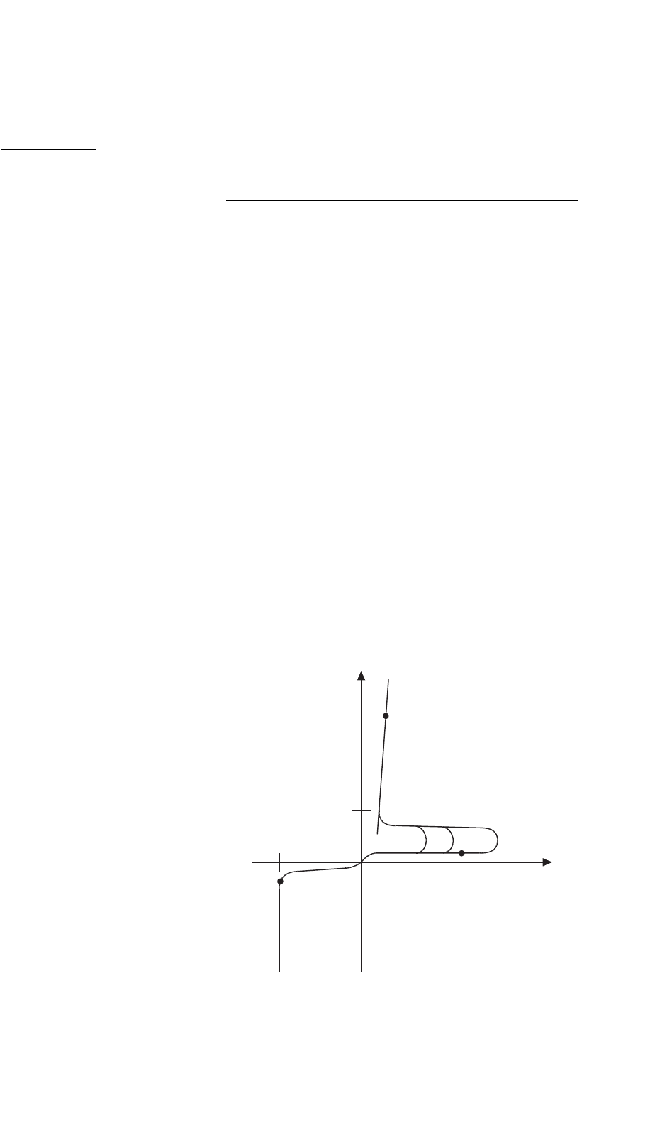
6.3.1 Current–Voltage Curves for Thyristors
A plot of the anode current (i
A
) as a function of anode–cathode
voltage (v
AK
) is shown in Fig. 6.3. The forward-blocking mode
is shown as the low-current portion of the graph (solid curve
around operating point “1”). With zero gate current and posi-
tive v
AK
, the forward characteristic in the off- or blocking-state
is determined by the center junction J
2
, which is reverse biased.
At operating point “1” very little current flows (I
co
only)
through the device. However, if the applied voltage exceeds
the forward-blocking voltage, the thyristor switches to its on-
or conducting-state (shown as operating point “2”) because of
carrier multiplication (M in Eq. (6.1)). The effect of gate cur-
rent is to lower the blocking voltage at which switching takes
place. The thyristor moves rapidly along the negatively-sloped
portion of the curve until it reaches a stable operating point
determined by the external circuit (point “2”). The portion
of the graph indicating forward-conduction shows the large
values of i
A
that may be conducted at relatively low values of
v
AK
, similar to a power diode.
As the thyristor moves from forward-blocking to forward-
conduction, the external circuit must allow sufficient anode
current to flow to keep the device latched. The minimum
anode current that will cause the device to remain in forward-
conduction as it switches from forward-blocking is called the
V
AK
I
L
I
H
i
A
V
RBD
I
G1
I
G2
I
G
=0
I
G2
> I
G1
V
FBD
2
1
3
FIGURE 6.3 Static characteristic i–v curve typical of thyristors.
6 Thyristors 93
latching current I
L
. If the thyristor is already in forward-
conduction and the anode current is reduced, the device can
move its operating mode from forward-conduction back to
forward-blocking. The minimum value of anode current nec-
essary to keep the device in forward-conduction after it has
been operating at a high anode current value is called the
holding current I
H
. The holding current value is lower than
the latching current value as indicated in Fig. 6.3.
The reverse thyristor characteristic, quadrant III of Fig. 6.3,
is determined by the outer two junctions (J
1
and J
3
), which
are reverse biased in this operating mode (applied v
AK
is neg-
ative). Symmetric thyristors are designed so that J
1
will reach
reverse breakdown due to carrier multiplication at an applied
reverse potential near the forward breakdown value (operating
point “3” in Fig. 6.3). The forward- and reverse-blocking junc-
tions are usually fabricated at the same time with a very long
diffusion process (10–50 h) at high temperatures (>1200
◦
C).
This process produces symmetric blocking properties. Wafer
edge termination processing causes the forward-blocking capa-
bility to be reduced to about 90% of the reverse-blocking
capability. Edge termination is discussed below. Asymmetric
devices are made to optimize forward-conduction and turn-
off properties, and as such reach reverse breakdown at a lower
voltage than that applied in the forward direction. This is
accomplished by designing the asymmetric thyristor with a
much thinner n-base than is used in symmetric structures. The
thin n-base leads to improved properties such as lower for-
ward drop and shorter switching times. Asymmetric devices
are generally used in applications when only forward volt-
ages (positive, v
AK
) are to be applied (including many inverter
designs).
The form of the gate-to-cathode i–v characteristic of SCRs,
GTOs and IGCTs is similar to that of a diode. With positive
gate bias, the gate–cathode junction is forward biased and per-
mits the flow of a large current in the presence of a low voltage
drop. When negative gate voltage is applied to an SCR, the
gate–cathode junction is reverse biased and prevents the flow
of current until the avalanche breakdown voltage is reached.
In a GTO or IGCT, a negative gate voltage is applied to pro-
vide a low impedance path for anode current to flow out of
the device instead of out the cathode. In this way the cathode
region (base–emitter junction of the equivalent npn transis-
tor) turns off, thus pulling the equivalent npn transistor out
of conduction. This causes the entire thyristor to return to its
blocking state. The problem with the GTO and IGCT is that
the gate-drive circuitry is typically required to sink 10–50%
(for the GTO) or 100% (for the IGCT) of the anode current
to achieve turn-off.
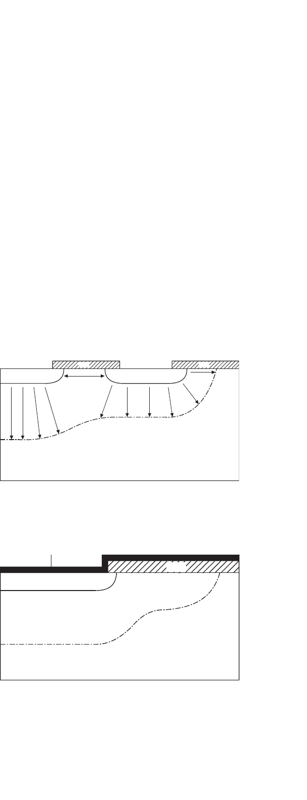
6.3.2 Edge and Surface Terminations
Thyristors are often made with planar diffusion technol-
ogy to create the cathode region. Formation of these
regions creates cylindrical curvature of the metallurgical
gate–cathode junction. Under reverse bias, the curvature of
the associated depletion region results in electric field crowd-
ing along the curved section of the p
+
diffused region. The field
crowding seriously reduces the breakdown potential below that
expected for the bulk semiconductor. A floating field ring, an
extra p diffused region with no electrical connection at the sur-
face, is often added to modify the electric field profile and thus
reduce it to a value below or at the field strength in the bulk.
An illustration of a single floating field ring is shown in Fig. 6.4.
The spacing, W, between the main anode region and the field
ring is critical. Multiple rings can also be employed to further
modify the electric field in high-voltage rated thyristors.
Another common method for altering the electric field at
the surface is by using a field plate as shown in cross section
in Fig. 6.5. By forcing the potential over the oxide to be the
same as at the surface of the p
+
region, the depletion region
can be extended so that the electric field intensity is reduced
near the curved portion of the diffused p
+
region. A common
practice is to use field plates with floating field rings to obtain
optimum breakdown performance.
High-voltage thyristors are made from single wafers of Si
and must have edge terminations other than floating field rings
or field plates to promote bulk breakdown and limit leakage
SiSiO
2
SiSiO
2
W
p
+
p
n
−
SiO
2
SiO
2
FIGURE 6.4 Cross section showing a floating field ring to decrease the
electric field intensity near the curved portion of the main anode region
(left-most p
+
region).
depletion boundary
p
+
n
−
A
SiO
2
FIGURE 6.5 Cross section showing a field plate used to reduce the
electric field intensity near the curved portion of the p
+
-region (anode).
94 A. Bryant et al.
n
+
p
n
−
p
FIGURE 6.6 Cross section of a thyristor showing the negative bevel
(upper p–n
−
and p–n
+
junctions) and positive bevel (lower p–n
−
junction) used for edge termination of large-area devices.
current at the surface. Controlled bevel angles can be created
using lapping and polishing techniques during production of
large-area thyristors. Two types of bevel junctions can be cre-
ated: (i) a positive bevel defined as one in which the junction
area decreases when moving from the highly-doped to the
lightly-doped side of the depletion region and (ii) a negative
bevel defined as one in which the junction area increases when
moving from the highly-doped to the lightly-doped side of
the depletion region. In practice, the negative bevel must be
lapped at an extremely shallow angle to reduce the surface field
below the field intensity in the bulk. All positive bevel angles
between 0 and 90
◦
result in a lower surface field than in the
bulk. Figure 6.6 shows the use of a positive bevel for the J
1
junction and a shallow negative bevel for the J
2
and J
3
junc-
tions on a thyristor cross section to make maximum use of
the Si area for conduction and still reduce the surface electric
field. Further details of the use of beveling, field plates, and
field rings can be found in Ghandi [2] and Baliga [3].
6.3.3 Packaging
Thyristors are available in a wide variety of packages, from
small plastic ones for low-power (i.e. TO-247), to stud-mount
FIGURE 6.7 Examples of thyristor packaging: stud-mount (left) and press-pack/capsule (right).
packages for medium-power, to press-pack (also called flat-
pack) for the highest power devices. The press-packs must
be mounted under pressure to obtain proper electrical and
thermal contact between the device and the external metal
electrodes. Special force-calibrated clamps are made for this
purpose. Large-area thyristors cannot be directly attached to
the large copper pole piece of the press-pack because of the
difference in the coefficient of thermal expansion (CTE), hence
the use of a pressure contact for both anode and cathode.
Figure 6.7 shows typical thyristor stud-mount and press-pack
packages.
Many medium power thyristors are appearing in mod-
ules where a half- or full-bridge (and associated anti-parallel
diodes) is put together in one package. A power module
package should have five characteristics:
i) electrical isolation of the baseplate from the semicon-
ductor;
ii) good thermal performance;
iii) good electrical performance;
iv) long life/high reliability; and
v) low cost.
Electrical isolation of the baseplate from the semiconductor
is necessary in order to contain both halves of a phase leg in
one package as well as for convenience (modules switching
different phases can be mounted on one heatsink) and safety
(heatsinks can be held at ground potential).
Thermal performance is measured by the maximum tem-
perature rise in the Si die at a given power dissipation level
with a fixed heat sink temperature. The lower the die temper-
ature, the better the package. A package with a low thermal
resistance from junction-to-sink can operate at higher power
densities for the same temperature rise or lower temperatures
for the same power dissipation than a more thermally resistive
package. While maintaining low device temperature is gener-
ally preferable, temperature variation affects majority carrier
and bipolar devices differently. Roughly speaking, in a bipo-
lar device such as a thyristor, switching losses increase and

6 Thyristors 95
TABLE 6.1 Thermal conductivity of thyristor package materials
Material Thermal conductivity
(W/m·K) at 300 K
Silicon 150
Copper (baseplate and pole pieces) 390–400
AlN substrate 170
Al
2
O
3
(Alumina) 28
Aluminum (Al) 220
Tungsten (W) 167
Molybdenum (Mo) 138
Metal matrix composites (MMC) 170
Thermal grease (heatsink compound) 0.75
60/40 solder (Pb/Sn eutectic) 50
95/5 solder (Pb/Sn high temperature) 35
conduction losses decrease with increasing temperature. In a
majority carrier device, such as a MOSFET, conduction losses
increase with increasing temperature. The thermal conductiv-
ity of typical materials used in thyristor packages is shown in
Table 6.1.
Electrical performance refers primarily to the stray induc-
tance in series with the die, as well as the capability of
mounting a low-inductance bus to the terminals. Another
problem is the minimization of capacitive cross-talk from one
switch to another, which can cause an abnormal on-state con-
dition by charging the gate of an off-state switch, or from a
switch to any circuitry in the package (as would be found in a
hybrid power module). Capacitive coupling is a major cause of
electromagnetic interference (EMI). As the stray inductance of
the module and the bus sets a minimum switching loss for the
device – because the switch must absorb the stored inductive
energy – it is very important to minimize inductance within the
module. Reducing the parasitic inductance reduces the high-
frequency ringing during transients that is another cause of
radiated electromagnetic interference. Since stray inductance
can cause large peak voltages during switching transients, min-
imizing it helps to maintain the device within its safe area of
operation.
Long life and high reliability are primarily attained through
minimization of thermal cycling, minimization of ambient
temperature, and proper design of the transistor stack. Ther-
mal cycling fatigues material interfaces because of coefficient of
thermal expansion (CTE) mismatch between dissimilar mate-
rials. As the materials undergo temperature variation, they
expand and contract at different rates which stresses the inter-
face between the layers and can cause interface deterioration
(e.g. cracking of solder layers or wire debonding). Chemical
degradation processes such as dendrite growth and impu-
rity migration are accelerated with increasing temperature, so
keeping the absolute temperature of the device low, as well as
minimizing the temperature changes to which it is subjected is
important. Typical CTE values for common package materials
are given in Table 6.2.
TABLE 6.2 CTE for thyristor package materials
Material CTE (mm/m·K) at 300 K
Silicon 4.1
Copper (baseplate and pole pieces) 17
AlN substrate 4.5
Al
2
O
3
(Alumina) 6.5
Tungsten (W) 4.6
Molybdenum (Mo) 4.9
Aluminum (Al) 23
Metal matrix composites (MMC) 5–20
60/40 solder (Pb/Sn eutectic) 25
Low cost is achieved in a variety of ways. Both man-
ufacturing and material costs must be taken into account
when designing a power module. Materials that are difficult
to machine or process, even if they are relatively cheap in
raw form (molybdenum, for example), should be avoided.
Manufacturing processes that lower yield also drive up costs.
In addition, a part that is very reliable can reduce future costs
by reducing the need for repair and replacement.
The basic half-bridge module has three power terminals:
plus, minus and phase. Advanced modules differ from tradi-
tional high power commercial modules in several ways. The
baseplate is metallized aluminum nitride (AlN) ceramic rather
than the typical 0.125” thick nickel-plated copper baseplate
with a soldered metallized ceramic substrate for electrical
isolation. This AlN baseplate stack provides a low thermal
resistance from die to heatsink. The copper terminal power
busses are attached by solder to the devices in a wirebond-free,
low-inductance, low-resistance, device interconnect configu-
ration. The balance of the assembly is typical for module
manufacturing with attachment of shells, use of dielectric gels,
and hard epoxies and adhesive to seal the finished module.
Details of the thermal performance of modules and advanced
modules can be found in Beker et al. [4] and Godbold et al. [5].
6.4 Dynamic Switching Characteristics
The time rate of rise of anode current (di/dt) during turn-on
and the time rate of rise of anode–cathode voltage (dv/dt) dur-
ing turn-off are important parameters to control for ensuring
proper and reliable operation. All thyristors have maximum
limits for di/dt and dv/dt that must not be exceeded. Devices
capable of conducting large currents in the on-state, are neces-
sarily made with large surface areas through which the current
flows. During turn-on, localized areas of a device (near the
gate region) begin to conduct current. The initial turn-on of
an SCR is shown in Fig. 6.8. The cross section illustrates how
injected gate current flows to the nearest cathode region, caus-
ing this portion of the npn transistor to begin conducting. The
pnp transistor then follows the npn into conduction such that
anode current begins flowing only in a small portion of the
96 A. Bryant et al.
Cathode
metallization
Anode
metallization
Gate
metallization
G
K
A
p
+
n
−
p
n
+
Cross-sectional
view
Top view
Gate
metallization
Cathode
metallization
FIGURE 6.8 Top view and associated cross section of gate–cathode
periphery showing initial turn-on region in a center-fired thyristor.
cathode region. If the local current density becomes too large
(in excess of several thousand amperes per square centime-
ter), then self-heating will damage the device. Sufficient time
(referred to as plasma spreading time) must be allowed for
the entire cathode area to begin conducting before the local-
ized currents become too high. This phenomenon results in a
maximum allowable rate of rise of anode current in a thyris-
tor and is referred to as a di/dt limit. In many high-frequency
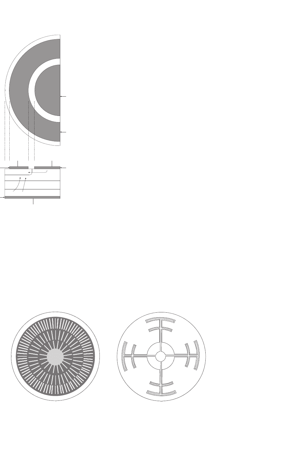
FIGURE 6.9 Top view of typical interdigitated gate–cathode patterns used for thyristors.
applications, the entire cathode region is never fully in con-
duction. Prevention of di/dt failure can be accomplished if the
rate of increase of conduction area exceeds the di/dt rate such
that the internal junction temperature does not exceed a speci-
fied critical temperature (typically approximately 350
◦
C). This
critical temperature decreases as the blocking voltage increases.
Adding series inductance to the thyristor to limit di/dt below
its maximum usually causes circuit design problems.
Another way to increase the di/dt rating of a device is to
increase the amount of gate–cathode periphery. Inverter SCRs
(so-named because of their use in high-frequency power con-
verter circuits that convert dc to ac, i.e. invert) are designed so
that there is a large amount of gate edge adjacent to a signifi-
cant amount of cathode edge. A top surface view of two typical
gate–cathode patterns, found in large thyristors, is shown in
Fig. 6.9. An inverter SCR often has a stated maximum di/dt
limit of approximately 2000 A/ms. This value has been shown
to be conservative [6], and by using excessive gate current
under certain operating conditions, an inverter SCR can be
operated reliably at 10,000 A/ms–20,000 A/ms.
A GTO takes the interdigitation of the gate and cathode to
the extreme (Fig. 6.9, left). In Fig. 6.10 a cross section of a
GTO shows the amount of interdigitation. A GTO often has
cathode islands that are formed by etching the Si. A metal plate
can be placed on the top to connect the individual cathodes
into a large arrangement of electrically parallel cathodes. The
gate metallization is placed so that the gate surrounding each
cathode is electrically in parallel as well. This construction not
only allows high di/dt values to be reached, as in an inverter
SCR, but also provides the capability to turn-off the anode
current by shunting it away from the individual cathodes and
out of the gate electrode upon reverse biasing of the gate.
During turn-off, current is decreasing while voltage across the
device is increasing. If the forward voltage becomes too high
while sufficient current is still flowing, then the device will
drop back into its conduction mode instead of completing its
turn-off cycle. Also, during turn-off, the power dissipation can
6 Thyristors 97
n
+
n
+
n
+
p
+
n
−
p
FIGURE 6.10 Cross section of a GTO showing the cathode islands and
interdigitation with the gate (p-base).
become excessive if the current and voltage are simultaneously
too large. Both of these turn-off problems can damage the
device as well as other portions of the circuit.
Another switching problem that occurs is associated pri-
marily with thyristors, though other power electronic devices
suffer some degradation of performance from the same prob-
lem. This problem is that thyristors can self-trigger into a
forward-conduction mode from a forward-blocking mode if
the rate of rise of forward anode–cathode voltage is too large.
This triggering method is due to displacement current through
the associated junction capacitances (the capacitance at J
2
dominates because it is reverse biased under forward applied
voltage). The displacement current contributes to the leakage
current I
co
, shown in Eq. (6.1). The SCRs, GTOs and IGCTs,
therefore, have a maximum dv/dt rating that should not be
exceeded (typical values are 100–1000 V/ms). Switching into a
reverse-conducting from a reverse-blocking state, due to an
applied reverse dv/dt, is not possible because the values of the
reverse α’s of the equivalent transistors can never be made
large enough to cause the necessary feedback (latching) effect.
An external capacitor is often placed between the anode and
cathode of the thyristor to help control the dv/dt experienced.
Capacitors and other components that are used to form such
protection circuits, known as snubbers, may be found in all
power semiconductor devices.
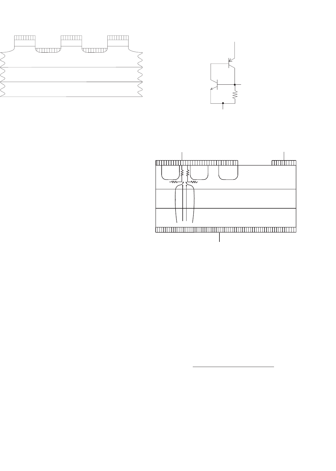
6.4.1 Cathode Shorts
As the temperature in the thyristor increases above 25
◦
C,
the minority carrier lifetime and the corresponding diffusion
lengths in the n- and p-bases increase. This leads to an increase
in the α’s of the equivalent transistors. Discussion of the details
of the minority carrier diffusion length and its role in deter-
mining the current gain factor α can be found in Sze [7].
Referring to Eq. (6.1), it is seen that a lower applied bias
will give a carrier multiplication factor M sufficient to switch
the device from forward-blocking into conduction, because of
this increase of the α’s with increasing temperature. Placing a
shunt resistor in parallel with the base–emitter junction of the
equivalent npn transistor (shown in Fig. 6.11) will result in an
effective current gain, α
neff
, that is lower than α
n
, as given by
G
A
K
α
p
R
s
α
n
FIGURE 6.11 Two-transistor equivalent circuit showing the addition of
a resistive shunt path for anode current.
KG
A
n
+
p
+
n
−
p
n
+
n
+
FIGURE 6.12 Cross section showing cathode shorts and the resulting
resistive shunt path for anode current.
Eq. (6.2), where v
GK
is the applied gate–cathode voltage, R
s
is
the equivalent lumped value for the distributed current shunt-
ing structure, and the remaining factors form the appropriate
current factor based on the applied bias and characteristics of
the gate–cathode junction. The shunt current path is imple-
mented by providing intermittent shorts, called cathode shorts,
between the p-base (gate) region and the n
+
-emitter (cathode)
region in the thyristor as illustrated in Fig. 6.12. The lumped
shunt resistance value is in the range of 1–15 as measured
from gate to cathode.
α
neff
= α
n
1
1 +(v
GK
α
n
)/(R
s
i
0
exp(qv
GK
/kT))
(6.2)
Low values of anode current (e.g. those associated with an
increase in temperature under forward-blocking conditions)
will flow through the shunt path to the cathode contact,
bypassing the n
+
-emitter and keeping the device out of its
forward-conduction mode. As the anode current becomes
98 A. Bryant et al.
large, the potential drop across the shunt resistance will be suf-
ficient to forward bias the gate–cathode junction, J
3
, and bring
the thyristor into forward-conduction. The cathode shorts
also provide a path for displacement current to flow with-
out forward biasing J
3
. The dv/dt rating of the thyristor is
thus improved as well as the forward-blocking characteristics
by using cathode shorts. However, the shorts do cause a low-
ering of cathode current handling capability because of the
loss of some of the cathode area (n
+
-region) to the shorting
pattern, an increase in the necessary gate current to obtain
switching from forward-blocking to forward-conduction, and
an increase in complexity of manufacturing of the thyristor.
The loss of cathode area due to the shorting-structure is from
5 to 20%, depending on the type of thyristor. By careful
design of the cathode short windows to the p-base, the hold-
ing current can be made lower than the latching current. This
is important so that the thyristor will remain in forward-
conduction when used with varying load impedances.
6.4.2 Anode Shorts
A further increase in forward-blocking capability can be
obtained by introducing anode shorts in addition to the cath-
ode shorts. This reduces α
p
in a similar manner that cathode
shorts reduce α
n
. An illustration of this is provided in Fig. 6.13.
In this structure both J
1
and J
3
are shorted (anode and cathode
shorts), so that the forward-blocking capability of the thyristor
is completely determined by the avalanche breakdown charac-
teristics of J
2
. Anode shorts will result in the complete loss of
reverse-blocking capability and is only suitable for thyristors
used in asymmetric circuit applications.
n+ n+ n+ n+
p+ p+ p+ p+
n
−
p
Shorted cathode Gate
n+ region
Shorted anode
FIGURE 6.13 Cross section showing integrated cathode and anode
shorts.
6.4.3 Amplifying Gate
The cathode-shorting structure will reduce the gate sensitiv-
ity dramatically. To increase this sensitivity and yet retain the
Metal anode contact
n+ n+ n+ n+
Main cathode areas
Cathode contact
Amplifying
gate
Pilot-gate
contact
Main I
A
Pilot I
A
p
n−
p
+
32
1
FIGURE 6.14 Cross section showing the amplifying gate structure in a
thyristor.
benefits of the cathode-shorts, a structure called an amplify-
ing gate (or regenerative gate) is used, as shown in Fig. 6.14
(and Fig. 6.9, right). When the gate current (1) is injected
into the p-base through the pilot-gate contact, electrons are
injected into the p-base by the n
+
-emitter with a given emit-
ter injection efficiency. These electrons traverse through the
p-base (the time taken for this process is called the transit
time) and accumulate near the depletion region. This nega-
tive charge accumulation leads to injection of holes from the
anode. The device then turns on after a certain delay, dic-
tated by the p-base transit time, and the pilot anode current
(2) begins to flow through a small region near the pilot-gate
contact as shown in Fig. 6.14.
This flow of pilot anode current corresponds to the ini-
tial sharp rise in the anode current waveform (phase I), as
shown in Fig. 6.15. The device switching then goes into phase
II, during which the anode current remains fairly constant,
suggesting that the resistance of the region has reached its
lower limit. This is due to the fact that the pilot anode current
(2) takes a finite time to traverse through the p-base laterally
and become the gate current for the main cathode area. The
n
+
-emitters start to inject electrons which traverse the p-base
vertically and after a certain finite time (transit time of the
p-base) reach the depletion region. The total time taken by the
lateral traversal of pilot anode current and the electron transit
time across the p-base is the reason for observing this charac-
teristic phase II interval. The width of the phase II interval is
comparable to the switching delay, suggesting that the p-base
transit time is of primary importance. Once the main cathode
region turns on, the resistance of the device decreases and the
anode current begins to rise again (transition from phase II to
III). From this time onward in the switching cycle, the plasma
spreading velocity will dictate the rate at which the conduction
area will increase. The current density during phase I and II
can be quite large, leading to a considerable increase in the
local temperature and device failure. The detailed effect of the
amplifying gate on the anode current rise will only be noticed
6 Thyristors 99
Phase II
PhaseI
Phase III
I
A
1.93 kA/division
100 ns/division
0
V
AK
500 V/division
FIGURE 6.15 Turn-on waveforms showing the effect of the amplifying
gate in the anode current rise.
at high levels of di/dt (in the range of 1000 A/ms), shown in
Fig. 6.15. It can be concluded that the amplifying gate will
increase gate sensitivity at the expense of some di/dt capability,
as demonstrated by Sankaran [8]. This lowering of di/dt capa-
bility can be somewhat off-set by an increase in gate–cathode
interdigitation as previously discussed.
6.4.4 Temperature Dependencies
The forward-blocking voltage of an SCR has been shown to be
reduced from 1350 V at 25
◦
Cto950Vat−175
◦
C in a near lin-
ear fashion [8]. Above 25
◦
C, the forward-blocking capability is
again reduced, due to changes in the minority carrier lifetime
which cause the leakage current to increase and the associ-
ated breakover voltage to decrease. Several dominant physical
parameters associated with semiconductor devices are sensi-
tive to temperature variations, causing their dependent device
characteristics to change dramatically. The most important of
these parameters are: (i) the minority carrier lifetimes (which
control the high-level injection lifetimes); (ii) the hole and
electron mobilities; (iii) the impact ionization collision cross
sections; and (iv) the free-carrier concentrations (primarily
the ionized impurity-atom concentration). Almost all of the
impurity atoms are ionized at temperatures above 0
◦
C, and
so further discussion of the temperature effects on ioniza-
tion is not relevant for normal operation. As the temperature
increases above 25
◦
C, the following trends are observed: the
carrier lifetimes increase, giving longer recovery times and
greater switching losses; the carrier mobilities are reduced,
increasing the on-state voltage drop; and at very high temper-
atures, the intrinsic carrier concentration becomes sufficiently
high that the depletion layer will not form and the device can-
not switch off. A more detailed discussion of these physical
parameters is beyond the scope of this article, but references
are listed for those persons interested in pursuing relevant
information about temperature effects.
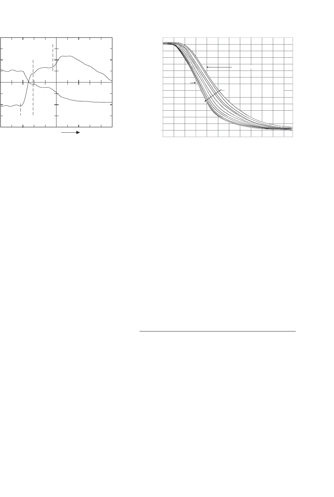
decreasing temperature (25°C steps)
–125°C (148K)
125°C (398K)
GROUND
2 A/division
4 µs/division
FIGURE 6.16 Temperature effect on the anode current tail during
turn-off.
It is well known that charge carrier recombination events
are more efficient at lower temperatures. This shows up as a
larger potential drop during forward-conduction and a shorter
recovery time during turn-off. A plot of the anode current
during turn-off, at various temperatures, for a typical GTO is
shown in Fig. 6.16.
An approximate relation between the temperature and the
forward drop across the n-base of a thyristor is discussed in
detail by Herlet [10] and Hudgins et al. [11]. Temperature
dependent equations relating the anode current density, J
A
and the applied anode–cathode voltage V
AK
are also given in
Reference [11]; these include the junction potential drops in
the device, the temperature dependence of the bandgap energy,
and the n-base potential drop. Data from measurements at
forward current densities of approximately 100 A/cm
2
on a
GTO rated for 1 kV symmetric blocking gives forward voltage
drops of 1.7 V at –50
◦
C and 1.8 V at 150
◦
C.
6.5 Thyristor Parameters
Understanding of a thyristor’s maximum ratings and electri-
cal characteristics is required for proper application. Use of
a manufacturer’s data sheet is essential for good design prac-
tice. Ratings are maximum or minimum values that set limits
on device capability. A measure of device performance under
specified operating conditions is a characteristic of the device.
A summary of some of the maximum ratings which must be
considered when choosing a thyristor for a given application
is provided in Table 6.3. Thyristor types shown in parenthe-
ses indicate a maximum rating unique to that device. Both
forward and reverse repetitive and non-repetitive voltage rat-
ings must be considered, and a properly rated device must
be chosen so that the maximum voltage ratings are never
exceeded. In most cases, either forward or reverse voltage

100 A. Bryant et al.
TABLE 6.3 Thyristor maximum ratings specified by manufacturers
Symbol Description
V
RRM
Peak repetitive reverse voltage
V
RSM
Peak non-repetitive reverse voltage (transient)
V
R(DC)
DC reverse blocking voltage
V
DRM
Peak repetitive forward off-state voltage
V
DSM
Peak non-repetitive forward off-state voltage
(transient)
V
D(DC)
DC forward-blocking voltage
I
T(RMS)
,I
F(RMS)
RMS forward on-state current
I
T
(AV ), I
F(AV )
Average forward on-state current at specified
case or junction temperature
I
TSM
,I
F(TSM )
Peak one-cycle surge on-state current (values
specified at 60 and 50 Hz)
I
TGQ
(GTO) Peak controllable current
I
2
t Non-repetitive pulse overcurrent capability
(t = 8.3 ms for a 60 Hz half cycle)
P
T
Maximum power dissipation
di/dt Critical rate of rise of on-state current at
specified junction temperature, gate current
and forward-blocking voltage
P
GM
(P
FGM
for GTO) Peak gate power dissipation (forward)
P
RGM
(GTO) Peak gate power dissipation (reverse)
P
G(AV )
Average gate power dissipation
V
FGM
Peak forward gate voltage
V
RGM
Peak reverse gate voltage
I
FGM
Peak forward gate current
I
RGM
(GTO) Peak reverse gate current
T
STG
Storage temperature
T
j
Junction operating temperature
V
RMS
Voltage isolation (modules)
transients in excess of the non-repetitive maximum ratings
result in destruction of the device. The maximum root mean
square (RMS) or average current ratings given are usually those
which cause the junction to reach its maximum rated temper-
ature. Because the maximum current will depend upon the
current waveform and upon thermal conditions external to
the device, the rating is usually shown as a function of case
temperature and conduction angle. The peak single half-cycle
surge-current rating must be considered, and in applications
where the thyristor must be protected from damage by over-
loads, a fuse with an I
2
t rating smaller than the maximum
rated value for the device must be used. Maximum ratings for
both forward and reverse gate voltage, current and power also
must not be exceeded.
The maximum rated operating junction temperature T
J
must not be exceeded, since device performance, in particular
voltage-blocking capability, will be degraded. Junction tem-
perature cannot be measured directly but must be calculated
from a knowledge of steady-state thermal resistance R
(J−C)
,
and the average power dissipation. For transients or surges,
the transient thermal impedance (Z
(J−C)
) curve must be
used (provided in manufacturer’s data sheets). The maxi-
mum average power dissipation P
T
is related to the maximum
rated operating junction temperature and the case tempera-
ture by the steady-state thermal resistance. In general, both
the maximum dissipation and its derating with increasing case
temperature are provided.
The number and type of thyristor characteristics specified
varies widely from one manufacturer to another. Some charac-
teristics are given only as typical values of minima or maxima,
while many characteristics are displayed graphically. Table 6.4
summarizes some of the typical characteristics provided as
maximum values. The maximum value means that the man-
ufacturer guarantees that the device will not exceed the value
given under the specified operating or switching conditions. A
minimum value means that the manufacturer guarantees that
the device will perform at least, as well as the characteristic
given under the specified operating or switching conditions.
Thyristor types shown in parenthesis indicate a characteris-
tic unique to that device. Gate conditions of both voltage
and current to ensure either non-triggered or triggered device
operation are included. The turn-on and turn-off transients
of the thyristor are characterized by switching times like the
TABLE 6.4 Typical thyristor characteristic maximum and minimum
values specified by manufacturers
Symbol Description
V
TM
,V
FM
Maximum on-state voltage drop(at specified
junction temperature and forward current)
I
DRM
Maximum forward off-state current (at specified
junction temperature and forward voltage)
I
RRM
Maximum reverse off-state current (at specified
junction temperature and reverse voltage)
dv/dt Minimum critical rate of rise of off-state voltage at
specified junction temperature and
forward-blocking voltage level
V
GT
Maximum gate trigger voltage (at specified
temperature and forward applied voltage)
V
GD
,V
GDM
Maximum gate non-trigger voltage (at specified
temperature and forward applied voltage)
I
GT
Maximum gate trigger current (at specified
temperature and forward applied voltage)
T
gt
(GTO) Maximum turn-on time (under specified switching
conditions)
T
q
Maximum turn-off time (under specified switching
conditions)
t
D
Maximum turn-on delay time (for specified test)
R
(J−C)
Maximum junction-to-case thermal resistance
R
(C−S)
Maximum case-to-sink thermal resistance
(interface lubricated)

6 Thyristors 101
turn-off time listed in Table 6.4. The turn-on transient can be
divided into three intervals: (i) gate-delay interval; (ii) turn-
on of initial area; and (iii) spreading interval. The gate-delay
interval is simply the time between application of a turn-
on pulse at the gate and the time the initial cathode area
turns on. This delay decreases with increasing gate drive cur-
rent and is of the order of a few microseconds. The second
interval, the time required for turn-on of the initial area, is
quite short, typically less than 1 ms. In general, the initial area
turned on is a small percentage of the total useful device area.
After the initial area turns on, conduction spreads (spreading
interval or plasma spreading time) throughout the device in
tens of microseconds for high-speed or thyristors. The plasma
spreading time may take up to hundreds of microseconds in
large-area phase-control devices.
Table 6.5 lists many of the thyristor parameters that appear
as listed values or as information on graphs. The definition of
each parameter and the test conditions under which they are
measured are given in the table as well.
6.6 Types of Thyristors
In recent years, most development effort has gone into con-
tinued integration of the gating and control electronics into
thyristor modules, and the use of MOS-technology to cre-
ate gate structures integrated into the thyristor itself. Many
variations of this theme are being developed and some tech-
nologies should rise above the others in the years to come.
Further details concerning most of the following discussion of
thyristor types can be found in [1].
6.6.1 SCRs and GTOs
The highest power handling devices continue to be bipolar
thyristors. High powered thyristors are large diameter devices,
some well in excess of 100 mm, and as such have a limita-
tion on the rate of rise of anode current, a di/dt rating. The
depletion capacitances around the p–n junctions, in particular
the center junction J
2
, limit the rate of rise in forward voltage
that can be applied even after all the stored charge, introduced
during conduction, is removed. The associated displacement
current under application of forward voltage during the thyris-
tor blocking state sets a dv/dt limit. Some effort in improving
the voltage hold-off capability and over-voltage protection
of conventional SCRs is underway by incorporating a lat-
eral high resistivity region to help dissipate the energy during
breakover. Most effort, though, is being placed in the further
development of high performance GTOs and IGCTs because of
their controllability and to a lesser extent in optically triggered
structures that feature gate circuit isolation.
High voltage GTOs with symmetric blocking capability
require thick n-base regions to support the high electric field.
The addition of an n+ buffer layer next to the p+-anode allows
high voltage forward-blocking and a low forward voltage drop
during conduction because of the thinner n-base required.
Cylindrical anode shorts have been incorporated to facilitate
excess carrier removal from the n-base during turn-off and still
retain the high blocking capability. This device structure can
control 200 A, operating at 900 Hz, with a 6 kV hold-off. Some
of the design tradeoff between the n-base width and turn-off
energy losses in these structures have been determined. A sim-
ilar GTO incorporating an n
+
-buffer layer and a pin structure
has been fabricated that can control up to 1 kA (at a forward
drop of 4 V) with a forward blocking capability of 8 kV. A
reverse conducting GTO has been fabricated that can block
6 kV in the forward direction, interrupt a peak current of 3 kA
and has a turn-off gain of about 5.
The IGCT is a modified GTO structure. It is designed and
manufactured so that it commutates all of the cathode current
away from the cathode region and diverts it out of the gate
contact. The IGCT is similar to a GTO in structure except that
it always has a low-loss n-buffer region between the n-base
and p-emitter. The IGCT device package is designed to result
in a very low parasitic inductance and is integrated with a
specially designed gate-drive circuit. The gate drive contains all
the necessary di/dt and dv/dt protection; the only connections
required are a low-voltage power supply for the gate drive and
an optical signal for controlling the gate. The specially designed
gate drive and ring-gate package circuit allows the IGCT to
be operated without a snubber circuit, and to switch with a
higher anode di/dt than a similar GTO. At blocking voltages
of 4.5 kV and higher the IGCT provides better performance
than a conventional GTO. The speed at which the cathode
current is diverted to the gate (di
GQ
/dt) is directly related to
the peak snubberless turn-off capability of the IGCT. The gate
drive circuit can sink current for turn-off at di
GQ
/dt values
in excess of 7000 A/ms. This hard gate drive results in a low
charge storage time of about 1 ms. The low storage time and
the fail-short mode makes the IGCT attractive for high-power,
high-voltage series applications; examples include high-power
converters in excess of 100 MVA, static vol-ampere reactive
(VAR) compensators and converters for distributed generation
such as wind power.
6.6.2 MOS-controlled Thyristors
The cross section of the p-type MCT unit cell is given in
Fig. 6.17. When the MCT is in its forward-blocking state and
a negative gate–anode voltage is applied, an inversion layer is
formed in the n-doped material that allows holes to flow lat-
erally from the p-emitter (p-channel FET source) through the
channel to the p-base (p-channel FET drain). This hole flow
is the base current for the npn transistor. The n-emitter then
injects electrons which are collected in the n-base, causing the
p-emitter to inject holes into the n-base so that the pnp tran-
sistor is turned on and latches the MCT. The MCT is brought