Power electronic handbook
Подождите немного. Документ загружается.


102 A. Bryant et al.
TABLE 6.5 Symbols and definitions of major thyristor parameters
R
θ
Thermal resistance Specifies the degree of temperature rise per unit of power, measuring
junction temperature from a specified external point. Defined when
junction power dissipation results in steady-state thermal flow.
R
θ(J−A)
Junction-to-ambient thermal resistance The steady-state thermal resistance between the junction and ambient.
R
θ(J−C)
Junction-to-case thermal resistance The steady-state thermal resistance between the junction and case surface.
R
θ(J−S)
Junction-to-sink thermal resistance The steady-state thermal resistance between the junction and the heatsink
mounting surface.
R
θ(C−S)
Contact thermal resistance The steady-state thermal resistance between the surface of the case and
the heatsink mounting surface.
Z
θ
Transient thermal impedance The change of temperature difference between two specified points or
regions at the end of a time interval divided by the step function
change in power dissipation at the beginning of the same interval
causing the change of temperature difference.
Z
θ(J−A)
Junction-to-ambient transient thermal
impedance
The transient thermal impedance between the junction and ambient.
Z
θ(J−C)
Junction-to-case transient thermal impedance The transient thermal impedance between the junction and the case
surface.
Z
θ(J−S)
Junction-to-sink transient thermal impedance The transient thermal impedance between the junction and the heatsink
mounting surface.
T
A
Ambient temperature It is the temperature of the surrounding atmosphere of a device when
natural or forced-air cooling is used, and is not influenced by heat
dissipation of the device.
T
S
Sink temperature The temperature at a specified point on the device heatsink.
T
C
Case temperature The temperature at a specified point on the device case.
T
J
Junction temperature The device junction temperature rating. Specifies the maximum and
minimum allowable operation temperatures.
T
STG
Storage temperature Specifies the maximum and minimum allowable storage temperatures
(with no electrical connections).
V
RRM
Peak reverse blocking voltage Within the rated junction temperature range, and with the gate terminal
open circuited, specifies the repetitive peak reverse anode to cathode
voltage applicable on each cycle.
V
RSM
Transient peak reverse-blocking voltage Within the rated junction temperature range, and with the gate terminal
open circuited, specifies the non-repetitive peak reverse anode to
cathode voltage applicable for a time width equivalent to less than 5 ms.
V
R(DC)
SCR only dc reverse-blocking voltage Within the rated junction temperature range, and with the gate terminal
open-circuited, specifies the maximum value for dc anode to cathode
voltage applicable in the reverse direction.
V
DRM
Peak forward-blocking voltage Within the rated junction temperature range, and with the gate terminal
open circuited (SCR), or with a specified reverse voltage between the
gate and cathode (GTO), specifies the repetitive peak off-state anode to
cathode voltage applicable on each cycle. This does not apply for
transient off-state voltage application.
V
DSM
Transient peak forward-blocking voltage Within the rated junction temperature range, and with the gate terminal
open circuited (SCR), or with a specified reverse voltage between the
gate and cathode (GTO), specifies the non-repetitive off-state anode to
cathode voltage applicable for a time width equivalent to less than
5 ms. This gives the maximum instantaneous value for non-repetitive
transient off-state voltage.
V
D(DC)
dc forward-blocking voltage Within the rated junction temperature range, and with the gate terminal
open circuited (SCR), or with a specified reverse voltage between the
gate and cathode (GTO), specifies the maximum value for dc anode to
cathode voltage applicable in the forward direction.
dv/dt Critical rate of rise of off-state voltage
dv/dt = (0.632V
D
)/τV
D
is specified off-state
voltage τ is time constant for exponential
At the maximum rated junction temperature range, and with the gate
terminal open circuited (SCR), or with a specified reverse voltage
between the gate and cathode (GTO), this specifies the maximum rate
of rise of off-state voltage that will not drive the device from an
off-state to an on-state when an exponential off-state voltage of
specified amplitude is applied to the device.
V
TM
Peak on-state voltage At specified junction temperature, and when on-state current (50 or
60 Hz, half sine wave of specified peak amplitude) is applied to the
device, indicates peak value for the resulting voltage drop.

6 Thyristors 103
TABLE 6.5—Contd.
I
T(RMS)
RMS on-state current At specified case temperature, indicates the RMS value for on-state
current that can be continuously applied to the device.
I
T(AV )
Average on-state current At specified case temperature, and with the device connected to a resistive
or inductive load, indicates the average value for forward-current (sine
half wave, commercial frequency) that can be continuously applied to
the device.
I
TSM
Peak on-state current Within the rated junction temperature range, indicates the peak-value for
non-repetitive on-state current (sine half wave, 50 or 60 Hz). This value
indicated for one cycle, or as a function of a number of cycles.
I
2
t Current-squared time The maximum, on-state, non-repetitive short-time thermal capacity of
the device and is helpful in selecting a fuse or providing a coordinated
protection scheme of the device in the equipment. This rating is
intended specifically for operation less than one half cycle of a 180°
(degree) conduction angle sinusoidal wave form. The off-state blocking
capability cannot be guaranteed at values near the maximum I
2
t.
di/dt Critical rate of Rise of on-state current At specified case temperature, specified off-state voltage, specified gate
conditions, and at a frequency of less than 60 Hz, indicates the
maximum rate of rise of on-state current which the thyristor will
withstand when switching from an off-state to an on-state, when using
recommended gate drive.
I
RRM
Peak reverse leakage current At maximum rated junction temperature, indicates the peak value for
reverse current flow when a voltage (sine half wave, 50 or 60 Hz, and
having a peak value as specified for repetitive peak reverse-voltage
rating) is applied in a reverse direction to the device.
I
DRM
Peak forward-leakage current At maximum rated junction temperature, indicates the peak value for
off-state current flow when a voltage (sine half wave, 50 or 60 Hz, and
having a peak value for repetitive off-state voltage rating) is applied in a
forward direction to the device. For a GTO, a reverse voltage between
the gate and cathode is specified.
P
GM
(SCR) P
GFM
(GTO)
Peak gate power dissipation peak gate forward
power dissipation
Within the rated junction temperature range, indicates the peak value for
maximum allowable power dissipation over a specified time period,
when the device is in forward-conduction between the gate and
cathode.
P
G(AV )
Average gate power dissipation Within the rated junction temperature range, indicates the average value
for maximum allowable power dissipation when the device is
forward-conducting between the gate and cathode.
P
GRM
GTO only Peak gate reverse power dissipation Within the rated junction temperature range, indicates the peak value for
maximum allowable power dissipation in the reverse direction between
the gate and cathode, over a specified time period.
P
GR(AV )
GTO only Average gate reverse power dissipation Within the rated junction temperature range, indicates the average value
for maximum allowable power dissipation in the reverse direction
between the gate and cathode.
I
GFM
Peak forward gate current Within the rated junction temperature range, indicates the peak value for
forward current flow between the gate and cathode.
I
GRM
GTO only Peak reverse gate current Within the rated junction temperature range, indicates peak value for
reverse current that can be conducted between the gate and cathode.
V
GRM
Peak reverse gate voltage Within the rated junction temperature range, indicates the peak value for
reverse voltage applied between the gate and cathode.
V
GFM
Peak forward gate voltage Within the rated junction temperature range, indicates the peak value for
forward voltage applied between the gate and cathode.
I
GT
Gate current to trigger At a junction temperature of 25°C, and with a specified off-voltage, and a
specified load resistance, indicates the minimum gate dc current
required to switch the thyristor from an off-state to an on-state.
V
GT
Gate voltage to trigger At a junction temperature of 25°C, and with a specified off-state voltage,
and a specified load resistance, indicates the minimum dc gate voltage
required to switch the thyristor from an off-state to an on-state.
V
GDM
SCR Only Non-triggering gate voltage At maximum rated junction temperature, and with a specified off-state
voltage applied to the device, indicates the maximum dc gate voltage
which will not switch the device from an off-state to an on-state.
I
TGQ
GTO only Gate controlled turn-off current Under specified conditions, indicates the instantaneous value for
on-current usable in gate control, specified immediately prior to device
turn-off.
continued
104 A. Bryant et al.
TABLE 6.5—Contd.
R
θ
Thermal resistance Specifies the degree of temperature rise per unit of power, measuring
junction temperature from a specified external point. Defined when
junction power dissipation results in steady-state thermal flow.
t
on
SCR only Turn-on time At specified junction temperature, and with a peak repetitive off-state
voltage of half rated value, followed by device turn-on using specified
gate current, and when specified on-state current of specified di/dt
flows, indicated as the time required for the applied off-state voltage to
drop to 10% of its initial value after gate current application. Delay time
is the term used to define the time required for applied voltage to drop
to 90% of its initial value following gate-current application. The time
required for the voltage level to drop from 90 to 10% of its initial value
is referred to as rise time. The sum of both these defines turn-on time.
T
q
SCR Only Turn-off time Specified at maximum rated junction temperature. Device set up to
conduct on-state current, followed by application of specified reverse
anode-cathode voltage to quench on-state current, and then increasing
the anode-cathode voltage at a specified rate of rise as determined by
circuit conditions controlling the point where the specified off-state
voltage is reached. Turn-off time defines the minimum time which the
device will hold its off-state, starting from the time on-state current
reached zero until the time forward voltage is again applied (i.e. applied
anode–cathode voltage becomes positive again).
t
gt
GTO only Turn-on time When applying forward current to the gate, indicates the time required to
switch the device from an off-state to an on-state.
t
qt
GTO only Turn-off time When applying reverse current to the gate, indicates the time required to
switch the device from an on-state to an off-state.
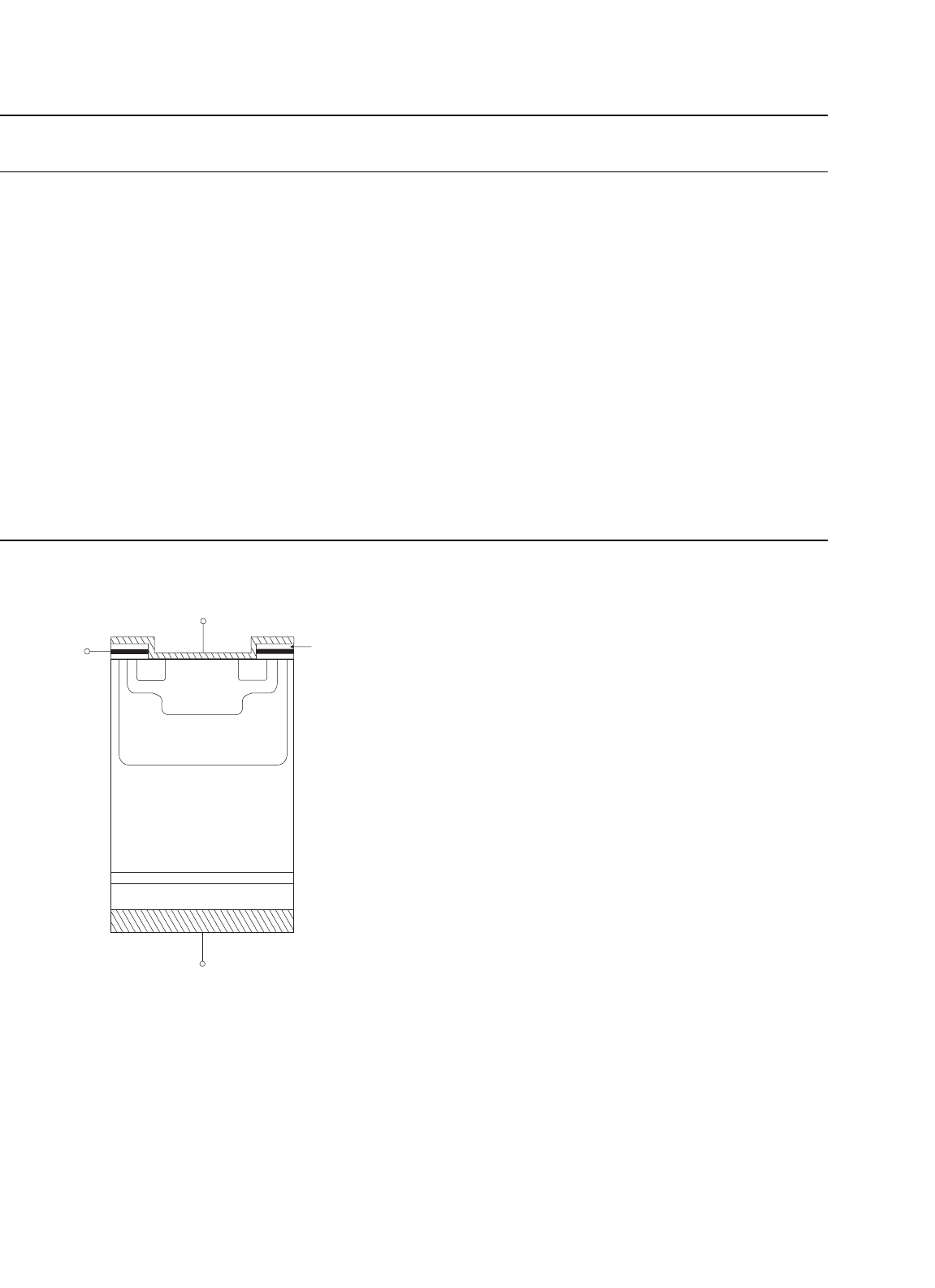
anode
p
n
+
n
+
p
+
gate
cathode
n
+
pp
p
−
n
−
oxide
FIGURE 6.17 Cross section of unit cell of a p-type MCT.
out of conduction by applying a positive gate–anode voltage.
This signal creates an inversion layer that diverts electrons in
the n-base away from the p-emitter and into the heavily doped
n-region at the anode. This n-channel FET current amounts
to a diversion of the pnp transistor base current so that its
base–emitter junction turns off. Holes are then no longer avail-
able for collection by the p-base. The elimination of this hole
current (npn transistor base current) causes the npn transis-
tor to turn-off. The remaining stored charge recombines and
returns the MCT to its blocking state.
The seeming variability in fabrication of the turn-off FET
structure continues to limit the performance of MCTs, par-
ticularly current interruption capability, though these devices
can handle two to five times the conduction current density
of IGBTs. Numerical modeling and its experimental verifi-
cation show that ensembles of cells are sensitive to current
filamentation during turn-off. All MCT device designs suffer
from the problem of current interruption capability. Turn-on
is relatively simple, by comparison; both the turn-on and con-
duction properties of the MCT approach the one-dimensional
thyristor limit.
Other variations on the MCT structure have been demon-
strated, namely the emitter switched thyristor (EST) and the
dual-gate emitter switched thyristor (DG-EST) [12]. These
comprise integrated lateral MOSFET structures which con-
nect a floating thyristor n-emitter region to an n+ thyristor
cathode region. The MOS channels are in series with the
floating n-emitter region, allowing triggering of the thyristor
with electrons from the n-base and interruption of the cur-
rent to initiate turn-off. The DG-EST behaves as a dual-mode
device, with the two gates allowing an IGBT mode to oper-
ate during switching and a thyristor mode to operate in the
on-state.
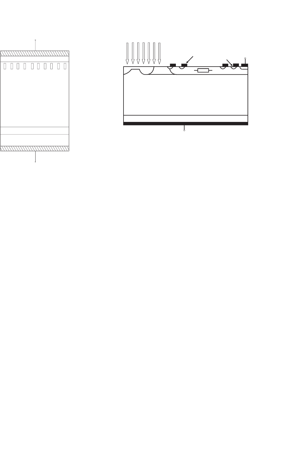
6 Thyristors 105
cathode
anode
n
+
n
−
buried gate (p
+
)
n
+
p
+
FIGURE 6.18 Cross section of a SITh or FCT.
6.6.3 Static Induction Thyristors
A SITh or FCTh has a cross section similar to that shown in
Fig. 6.18. Other SITh configurations have surface gate struc-
tures. The device is essentially a pin diode with a gate structure
that can pinch-off anode current flow. High power SIThs have
a sub-surface gate (buried-gate) structure to allow larger cath-
ode areas to be utilized, and hence larger current densities are
possible.
Planar gate devices have been fabricated with blocking capa-
bilities of up to 1.2 kV and conduction currents of 200 A, while
step-gate (trench-gate) structures have been produced that are
able to block up to 4 kV and conduct 400 A. Similar devices
with a “Verigrid” structure have been demonstrated that can
block 2 kV and conduct 200 A, with claims of up to 3.5 kV
blocking and 200 A conduction. Buried-gate devices that block
2.5 kV and conduct 300 A have also been fabricated. Recently
there has been a resurgence of interest in these devices for
fabrication in SiC.
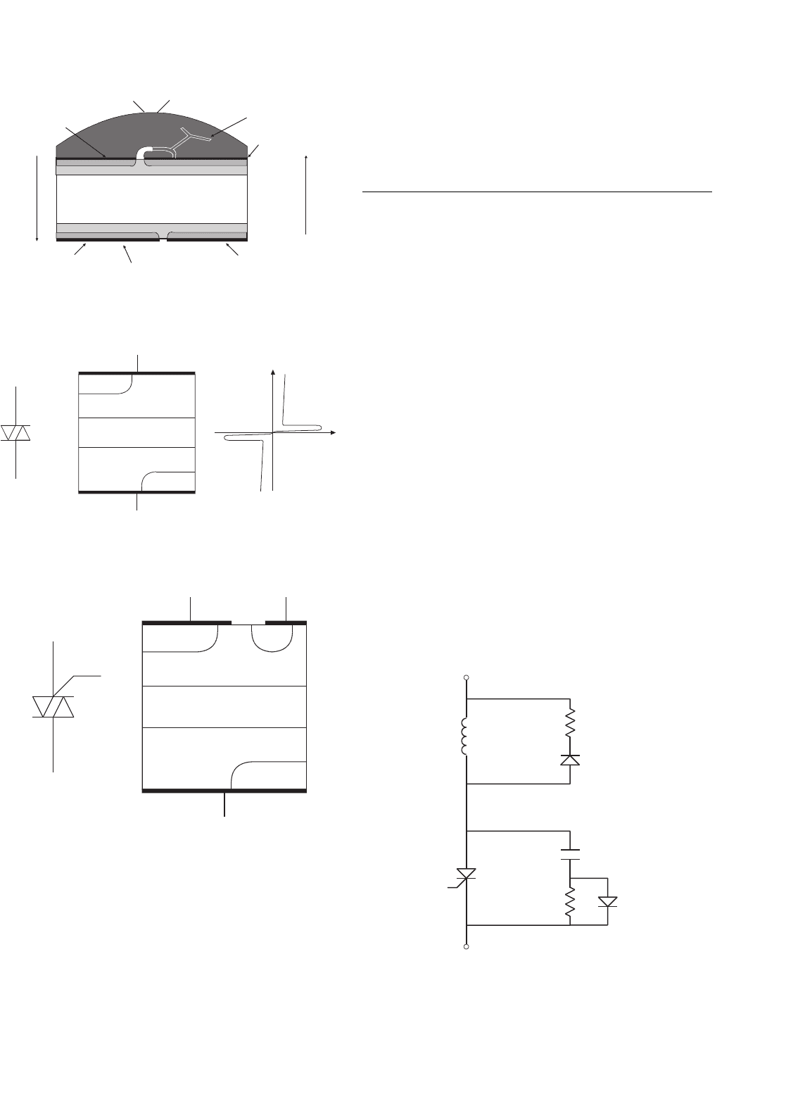
6.6.4 Optically Triggered Thyristors
Optically gated thyristors have traditionally been used in power
utility applications where series stacks of devices are neces-
sary to achieve the high voltages required. Isolation between
gate drive circuits for circuits such as static VAR compen-
sators and high voltage dc to ac inverters (for use in high
voltage dc (HVDC) transmission) have driven the develop-
ment of this class of devices, which are typically available in
ratings from 5 to 8 kV. The cross section is similar to that
shown in Fig. 6.19, showing the photosensitive region and the
light
n
−
p
−
p
n
+
K
A
p
R
amplifying gate
structures
FIGURE 6.19 Cross section of a light-triggered thyristors (LTT).
amplifying gate structures. Light-triggered thyristors (LTTs)
may also integrate over-voltage protection.
One of the most recent devices can block 6 kV forward and
reverse, conduct 2.5 kA average current, maintain a di/dt capa-
bility of 300 A/ms and a dv/dt capability of 3000 V/ms, with a
required trigger power of 10 mW. An integrated light triggered
and light quenched SITh has been produced that can block
1.2 kV and conduct up to 20 A (at a forward drop of 2.5 V).
This device is an integration of a normally off buried-gate
static induction photo-thyristor and a normally off p-channel
darlington surface-gate static induction phototransistor. The
optical trigger and quenching power required is less than 5
and 0.2 mW, respectively.
6.6.5 Bi-directional Thyristors
The BCT is an integrated assembly of two anti-parallel thyris-
tors on one Si wafer. The intended applications for this switch
are VAR compensators, static switches, soft starters and motor
drives. These devices are rated up to 6.5 kV blocking. Cross-
talk between the two halves has been minimized. A cross
section of the BCT is shown in Fig. 6.20. Note that each
surface has a cathode and an anode (opposite devices). The
small gate–cathode periphery necessarily restricts the BCT to
low-frequency applications because of its di/dt limit.
Low-power devices similar to the BCT, but in existence for
many years, are the diac and triac. A simplified cross section
of a diac is shown in Fig. 6.21. A positive voltage applied to
the anode with respect to the cathode forward biases J
1
, while
reverse biasing J
2
.J
4
and J
3
are shorted by the metal con-
tacts. When J
2
is biased to breakdown, a lateral current flows
in the p
2
region. This lateral flow forward biases the edge
of J
3
, causing carrier injection. The result is that the device
switches into its thyristor mode and latches. Applying a reverse
voltage causes the opposite behavior at each junction, but
106 A. Bryant et al.
Separation
region
Thyristor half
B
Thyristor half
A
Anode B
Gate A
Cathode A
Shallow p-base
Deep p-base
n-base
Deep p-base
Shallow p-base
Anode A
Cathode B
Gate B
(not visible)
V
B
(t)
V
A
(t)
FIGURE 6.20 Cross section of a bi-directional control thyristor (BCT).
v
i
n
1
p
1
n
2
n
3
p
2
K
A
A
K
J1
J2
J3
J4
FIGURE 6.21 Cross section and i–v plot of a diac.
n
−
p
n
+
n
+
p
n
MT2
G
MT1
G
MT1
MT2
FIGURE 6.22 Cross section of a triac.
with the same result. Figure 6.21 also shows the i–v plot for
a diac.
The addition of a gate connection, to form a triac, allows
the breakover to be controlled at a lower forward voltage.
Figure 6.22 shows the structure for the triac. Unlike the diac,
this is not symmetrical, resulting in differing forward and
reverse breakover voltages for a given gate voltage. The device
is fired by applying a gate pulse of the same polarity relative to
MT1 as that of MT2.
6.7 Gate Drive Requirements
6.7.1 Snubber Circuits
To protect a thyristor, from a large di/dt during turn-on and
a large dv/dt during turn-off, a snubber circuit is needed.
A general snubber topology is shown in Fig. 6.23. The turn-on
snubber is made by inductance L
1
(often L1 is stray inductance
only). This protects the thyristor from a large di/dt during the
turn-on process. The auxiliary circuit made by R
1
and D
1
allows the discharging of L
1
when the thyristor is turned off.
The turn-off snubber is made by resistor R
2
and capacitance
C
2
. This circuit protects a GTO from large dv/dt during the
turn-off process. The auxiliary circuit made by D
2
and R
2
allows the discharging of C
2
when the thyristor is turned on.
The circuit of capacitance C
2
and inductance L
1
also limits the
value of dv/dt across the thyristor during forward-blocking. In
addition, L
1
protects the thyristor from reverse over-currents.
R
1
and diodes D
1
,D
2
are usually omitted in ac circuits with
converter-grade thyristors. A similar second set of L, C and R
may be used around this circuit in HVDC applications.
6.7.2 Gate Circuits
It is possible to turn on a thyristor by injecting a current pulse
into its gate. This process is known as gating, triggering or
firing the thyristor. The most important restrictions are on
the maximum peak and duration of the gate pulse current.
R
2
D
2
C
2
D
1
R
1
L
1
Thyristor
FIGURE 6.23 Turn-on (top elements) and turn-off (bottom elements)
snubber circuits for thyristors.
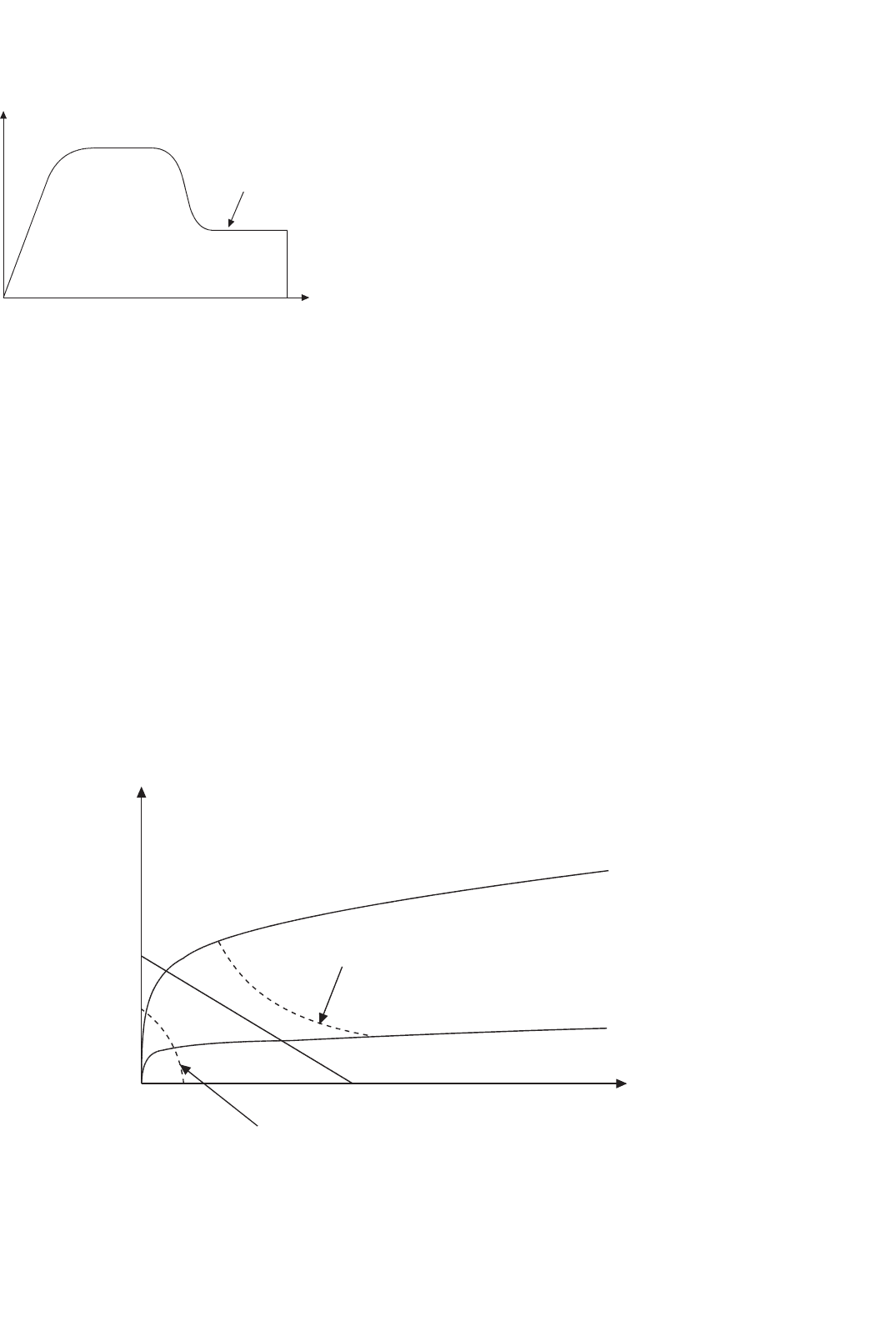
6 Thyristors 107
0
i
g
(t)
t
Back-porch current
FIGURE 6.24 Gate current waveform showing large initial current
followed by a suitable back-porch value.
In order to allow a fast turn-on, and a correspondingly large
anode di/dt during the turn-on process, a large gate current
pulse is supplied during the initial turn-on phase with a large
di
G
/dt. The gate current is kept on, at lower value, for some
times after the thyristor turned on in order to avoid unwanted
turn-off of the device; this is known as the “back-porch” cur-
rent. A shaped gate current waveform of this type is shown in
Fig. 6.24.
Figure 6.25 shows typical gate i–v characteristics for the
maximum and minimum operating temperatures. The dashed
line represents the minimum gate current and corresponding
gate voltage needed to ensure that the thyristor will be triggered
at various operating temperatures. It is also known as the locus
of minimum firing points. On the data sheet it is possible find a
line representing the maximum operating power of the thyris-
tor gating internal circuit. The straight line, between V
GG
and
T
j
= –40 °C
T
j
= 150 °C
Minimum gate current to trigger
I
G
V
GK
0
V
G
/R
G
V
G
Maximum gate power dissipation
FIGURE 6.25 Gate i–v curve for a typical thyristor.
V
GG
/R
G
, represents the current voltage characteristic of the
equivalent trigger circuit. If the equivalent trigger circuit line
intercepts the two gate i–v characteristics for the maximum
and minimum operating temperatures between where they
intercept the dashed lines (minimum gate current to trigger
and maximum gate power dissipation), then the trigger circuit
is able to turn-on the thyristor at any operating temperature
without destroying or damaging the device.
In order to keep the power circuit and the control circuit
electrically unconnected, the gate signal generator and the gate
of the thyristor are often connected through a transformer.
There is a transformer winding for each thyristor, and in
this way unwanted short circuits between devices are avoided.
A general block diagram of a thyristor gate-trigger circuit is
shown in Fig. 6.26. This application is for a standard bridge
configuration often used in power converters.
Another problem can arise if the load impedance is high,
particularly if the load is inductive and the supply voltage is
low. In this situation, the latching current may not be reached
during the trigger pulse. A possible solution to this problem
could be the use of a longer current pulse. However, such a
solution is not attractive because of the presence of the isola-
tion transformer. An alternative solution is the generation of a
series of short pulses that last for the same duration as a single
long pulse. A single short pulse, a single long pulse and a series
of short pulses are shown in Fig. 6.27. Reliable gating of the
thyristor is essential in many applications.
There are many gate trigger circuits that use optical iso-
lation between the logic-level electronics and a drive stage
(typically MOSFETs) configured in a push–pull output. The
dc power supply voltage for the drive stage is provided
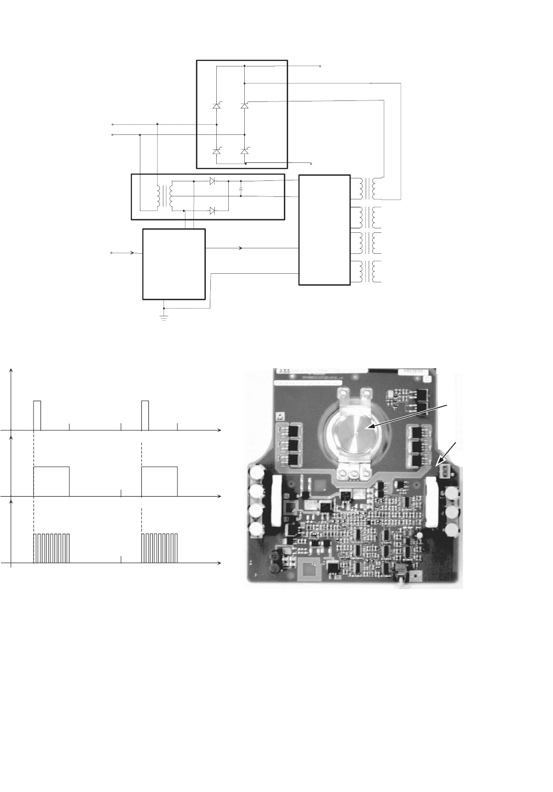
108 A. Bryant et al.
Zero-Crossing
Detection and
Phase-Angle
Circuit
Current
Amplifier
Input Control Signal
Isolation Transformers
for Gate Trigger Signal
DC Power Supply for
Current Amplifier Circuit
AC Line Voltage
T1
T2
T3
T4
Out to T1
Out to T4
Out to T2
Out to T3
Power
Converter
FIGURE 6.26 Block diagram of a transformer-isolated gate drive circuit.
2p
2p
a + 2p
0
a
a
ap
p
p
0
0
i
G
i
G
i
G
(a)
(b)
(c)
2p
3p
3p
3p
w
t
a + 2p
a + 2pw
t
w
t
FIGURE 6.27 Multiple gate pulses used as an alternative to one long
current pulse.
through transformer isolation. Many device manufacturers
supply drive circuits available on printed circuit (PC) boards
or diagrams of suggested circuits.
IGCT gate drives consist of an integrated module to which
the thyristor is connected via a low-inductance mounting;
an example is given in Fig. 6.28. Multiple MOSFETs and
GCT
Gate unit
FIGURE 6.28 Typical layout of an IGCT gate drive.
capacitors connected in parallel may be used to source or sink
the necessary currents to turn the device on or off. Logic in the
module controls the gate drive from a fiber-optic trigger input,
and provides diagnostic feedback from a fiber-optic output.
A simple power supply connection is also required.
6 Thyristors 109
6.8 PSpice Model
Circuit simulators such as Spice and PSpice are widely used
as tools in the design of power systems. For this purpose
equivalent circuit models of thyristors have been developed. A
variety of models have been proposed with varying degrees of
complexity and accuracy. Frequently the simple two-transistor
model described in Section 6.2 is used in PSpice. This simple
structure, however, cannot model the appropriate negative-
differential-resistance (NDR) behavior as the thyristor moves
from forward-blocking to forward-conduction. Few other
models for conventional thyristors have been reported. A
PSpice model for a GTO has been developed by Tsay et al. [13],
which captures much of thyristor behavior, such as the static
i–v curve shown in Fig. 6.3, dynamic characteristics (turn-on
and turn-off times), device failure modes (e.g. current crowd-
ing due to excessive di/dt at turn-on and spurious turn-on
due to excessive dv/dt at turn-off), and thermal effects. Specif-
ically, three resistors are added to the two-transistor model to
create the appropriate behavior.
The proposed two-transistor, three-resistor model (2T-3R)
is shown in Fig. 6.29. This circuit exhibits the desired NDR
behavior. Given the static i–v characteristics for an SCR or
GTO, it is possible to obtain similar curves from the model by
choosing appropriate values for the three resistors and for the
forward current gains α
p
and α
n
of the two transistors. The
process of curve fitting can be simplified by keeping in mind
that resistor R
1
tends to affect the negative slope of the i–v
characteristic, resistor R
2
tends to affect the value of the hold-
ing current I
H
and resistor R
3
tends to affect the value of the
forward breakdown voltage V
FBD
. When modeling thyristors
with cathode or anode shorts, as described in Section 6.4, the
presence of these shorts determines the values of R
1
and R
2
,
K
i
G
i
A
i
I
Ai
R
2i
R
3i
R
1i
NPN
Q
2i
I
Gi
PNP
Q
1i
FIGURE 6.29 A two-transistor, three-resistor model for SCRs and
GTOs.
respectively. In the case of a GTO or IGCT, an important
device characteristic is the so-called turn-off gain K
off
=I
A
/|I
G
|,
i.e. the ratio of the anode current to the negative gate cur-
rent required to turn-off the device. An approximate formula
relating the turn-off gain to the α‘s of the two transistors is
given by,
K
off
=
α
n
α
n
+α
p
−1
(6.3)
The ability of this model to predict dynamic effects depends
on the dynamics included in the transistor models. If transis-
tor junction capacitances are included, it is possible to model
the dv/dt limit of the thyristor. Too high a value of dv
AK
/dt
will cause significant current to flow through the J
2
junction
capacitance. This current acts like gate current and can turn
on the device.
This model does not accurately represent spatial effects such
as current crowding at turn-on (the di/dt limit), when only part
of the device is conducting, and, in the case of a GTO, cur-
rent crowding at turn-off, when current is extracted from the
gate to turn-off the device. Current crowding is caused by the
location of the gate connection with respect to the conduct-
ing area of the thyristor and by the magnetic field generated
by the changing conduction current. To model these effects,
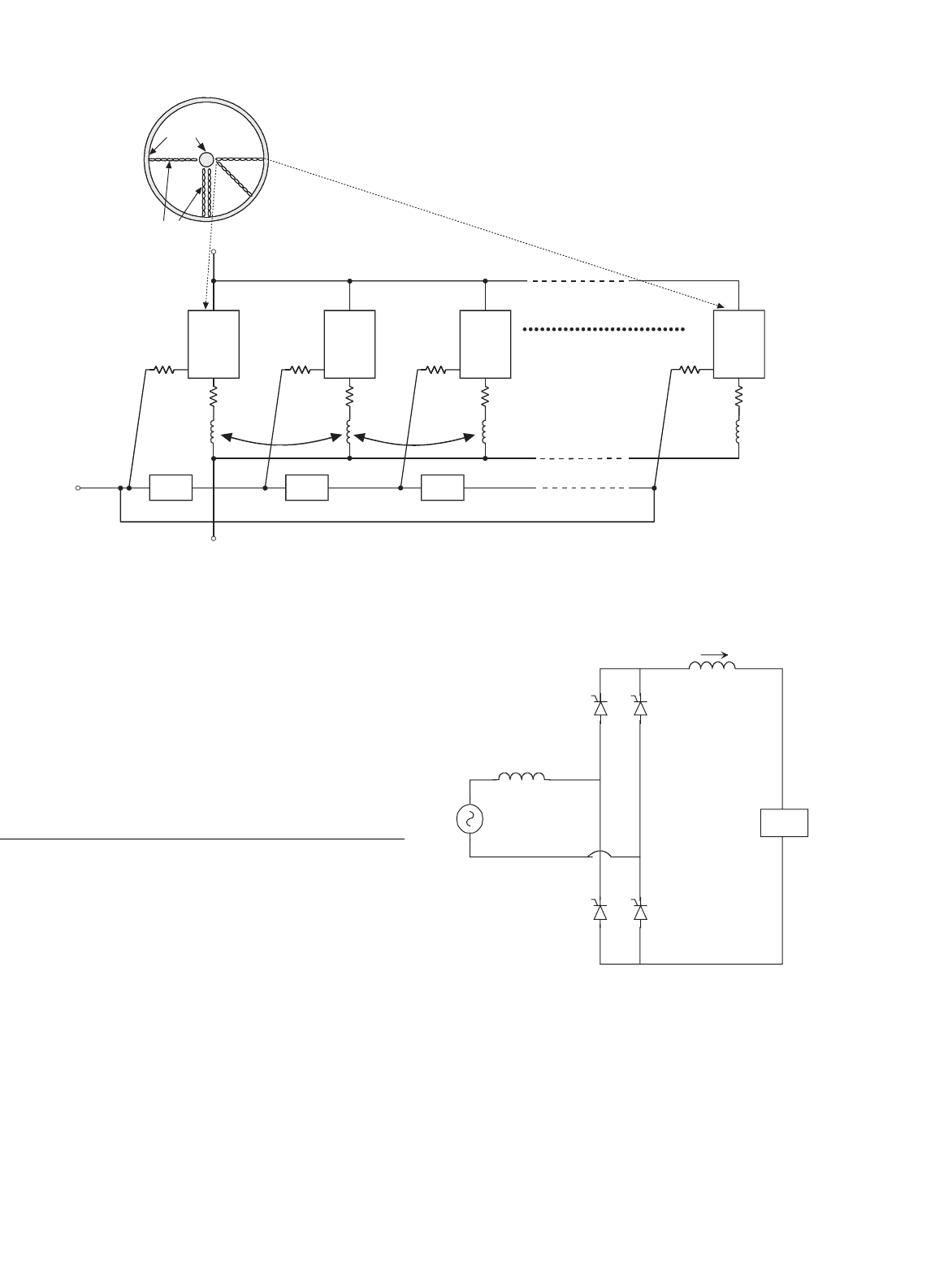
Tsay et al. [13] propose a multi-cell circuit model, in which the
device is discretized in a number of conducting cells, each hav-
ing the structure of Fig. 6.29. This model, shown in Fig. 6.30,
takes into account the mutual inductive coupling, the delay in
the gate turn-off signal due to positions of the cells relative
to the gate connection, and non-uniform gate- and cathode-
contact resistance. In particular, the RC delay circuits (series R
with a shunt C tied to the cathode node) model the time delays
between the gate triggering signals due to the position of the
cell with respect to the gate connection; coupled inductors, M,
model magnetic coupling between cells; resistors, R
KC
, model
non-uniform contact resistance; and resistors, R
GC
, model gate
contact resistances. The various circuit elements in the model
can be estimated from device geometry and measured elec-
trical characteristics. The choice of the number of cells is a
tradeoff between accuracy and complexity. Example values of
the RC delay network, R
GC
, R
KC
, and M are given in Table 6.6.
Other GTO thyristor models have been developed which
offer improved accuracy at the expense of increased complex-
ity. The model by Tseng et al. [14] includes charge storage
TABLE 6.6 Element values for each cell of a multi-cell GTO model
Model component Symbol Value
Delay resistor R 1 m
Delay capacitor C 1nF
Mutual coupling inductance M 10 nH
Gate contact resistance R
GC
1m
Cathode contact resistance R
KC
1m
110 A. Bryant et al.
Cell
Model
1
Cell
Model
2
R
GC1
R
GC2
R
GC3
R
GC8
R
KC1
R
KC2
R
KC3
R
KC8
Delay
Circuit
Delay
Circuit
Delay
Circuit
M
12
M
23
K
1
K
2
K
3
K
8
A
8
A
3
A
2
A
1
G
1
G
2
G
3
G
8
Gate
Cathode
Anode
Gate
Islands
(Cathode)
Cell
Model
3
Cell
Model
8
FIGURE 6.30 Thyristor multi-cell circuit model containing eight cells.
effects in the n-base, and its application to a multi-cell model,
as in Fig. 6.30, has been demonstrated successfully. Models
for the IGCT, based on the lumped-charge approach [15] and
the Fourier-based solution of the ambipolar diffusion equation
(ADE) [16], have also been developed.
6.9 Applications
The most important application of thyristors is for line-
frequency phase-controlled rectifiers. This family includes
several topologies, of which one of the most important is
used to construct HVDC transmission systems. A single-phase
controlled rectifier is shown in Fig. 6.31.
The use of thyristors instead of diodes allows the average
output voltage to be controlled by appropriate gating of the
thyristors. If the gate signals to the thyristors were contin-
uously applied, the thyristors in Fig. 6.31 would behave as
diodes. If no gate currents are supplied they behave as open
circuits. Gate current can be applied any time (phase delay)
after the forward voltage becomes positive. Using this phase-
control feature, it is possible to produce an average dc output
voltage less than the average output voltage obtained from an
uncontrolled diode rectifier.
Load
L
s
v
s
+
−
+
−
L
d
i
d
v
d
FIGURE 6.31 Single-phase controlled rectifier circuit.
6.9.1 DC–AC Utility Inverters
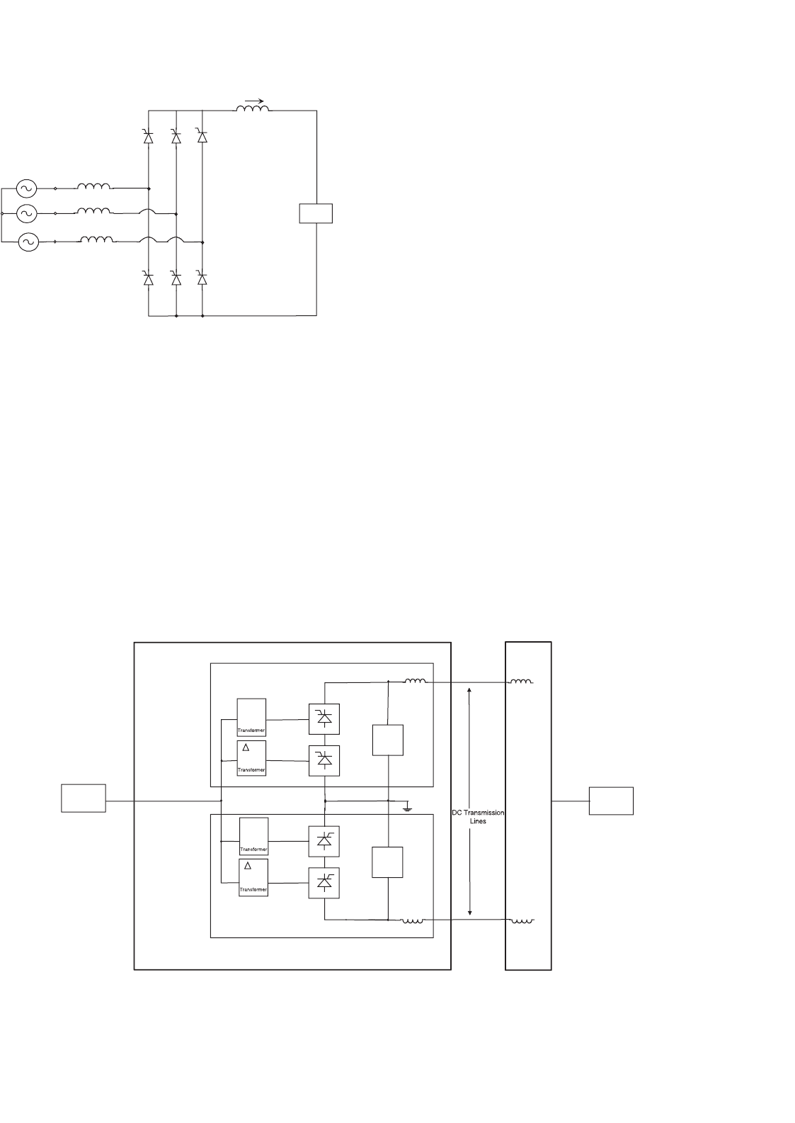
Three-phase converters can be made in different ways, accord-
ing to the system in which they are employed. The basic circuit
used to construct these topologies – the three-phase controlled
rectifier – is shown in Fig. 6.32.
6 Thyristors 111
Load
L
s
+
−
L
r
i
r
v
r
n
a
v
an
+−
L
s
L
s
b
c
v
bn
v
cn
+
+
−
−
FIGURE 6.32 A three-phase controlled bridge circuit used as a basic
topology for many converter systems.
Starting from this basic configuration, it is possible to con-
struct more complex circuits in order to obtain high-voltage
or high-current outputs, or just to reduce the output ripple by
constructing a multi-phase converter. One of the most impor-
tant systems using the topology shown in Fig. 6.32 as a basic
circuit is the HVDC system represented in Fig. 6.33. This sys-
tem is made by two converters, a transmission line, and two ac
systems. Each converter terminal is made of two poles. Each
pole is made by two six-pulse line-frequency converters con-
nected through -Y and Y-Y transformers in order to obtain a
twelve-pulse converter and a reduced output ripple. The filters
AC Power
Grid #2
Filter
Filter
Y Y
Y
Converter #2
12-pulse Converter
for Positive Line
AC Power
Grid #1
Converter #1
12-pulse Converter
for Negative Line
Y
Y Y
FIGURE 6.33 A HVDC transmission system.
are required to reduce the current harmonics generated by the
converter.
When a large amount of current and relatively low volt-
age is required, it is possible to connect in parallel, using a
specially designed inductor, two six-pulse line-frequency con-
verters connected through -Y and Y-Y transformers. The
special inductor is designed to absorb the voltage between the
two converters, and to provide a pole to the load. This topol-
ogy is shown in Fig. 6.34. This configuration is often known as
a twelve-pulse converter. Higher pulse numbers may also be
found.
6.9.2 Motor Control
Another important application of thyristors is in motor control
circuits. Historically thyristors have been used heavily in trac-
tion, although most new designs are now based on IGBTs.
Such motor control circuits broadly fall into four types:
i) chopper control of a dc motor from a dc supply; ii) single-
or three-phase converter control of a dc motor from an ac
supply; iii) inverter control of an ac synchronous or induction
machine from a dc supply and iv) cycloconverter control of an
ac machine from an ac supply. An example of a GTO chopper
is given in Fig. 6.35. L
1
, R
1
,D
1
, and C
1
are the turn-on snub-
ber; R
2
,D
2
, and C
2
are the turn-off snubber; finally R
3
and
D
3
form the snubber for the freewheel diode D
3
. A thyristor
cycloconverter is shown in Fig. 6.36; the waveforms show the
fundamental component of the output voltage for one phase.
Three double converters are used to produce a three-phase