Power electronic handbook
Подождите немного. Документ загружается.

794 V. K. Sood
A
A
B
B
C
C
D
D
1 1
2 2
Rectifier
11th
13th
L=44 mH
Rectifier AC Filters
Inverter AC Filters
11th
13th
Things to do:
1. Add DC line
DC Filter
DC Filter
Rectifier AC system
Inverter AC
system
Bi-polar 12p HVDC transmission system
Rectifier: +/- 500 kV, 1.5 kA, Alpha = 18 degs, Ld = 350 mH
Inverter: +/- 490 kV, 1.5 kA, Gamma = 18 degs, Ld = 350 mH
AC: 230 kV L-L on Line Side; 205.45 kV L-L on Valve Side.
Transformers with 10% Leakage Reactance per phase.
Thevenin Sources At Rec and Inv.
Timestep = Use 25 micro-sec.
For information: V.K.Sood, v.sood@ieee.org
DC Line
+ Pole
- Pole
1 Ph fault
amplitude 1.0 pu
width 200 ms
time shift 300 ms
Following tests have been pre-programmed and tested:
1. 10% step change in I order at rectifier
2. 10% step change in Gamma order at inverter
3. Commutation failure at inverter
4. Single phase fault at rectifier showing mode shift
+
2.5
+
350mH
scope
id_rec
v(t)
p2
+
RL1
1.1572,22.58mH
+
C2
12.536uF
+
239kVRMSLL /_67.43
?v
+
RL2
1.1572,22.58mH
+
220.0kVRMSLL /_67.43
?v
v(t)
p3
scope
V_pri_rec_a
scope
V_pri_inv_a
3-phase
+
-
gates
6-pulse bridge
REC_STAR_PLUS
+
350mH
+
2.5
v(t) i(t)
p1
+
1uF
!v
C5
+
195.4mH
L5
+
10.35
R5
RLC +
RLC +
VV1
VV2
VV3
VV4
VV5
VV6
Gamma_min
Gamma Detector
V.K.Sood
DEV3
1
2
3
4
5
6
dc_pos
dc_neg f3
f6
f2
f5
Pac
f1
f4
VV1
VV3
VV5
VV4
VV6
VV2
VC1
VC3
VC5
VC4
VC6
VC2
Bridge
6p_Bridge
INV_STAR_PLUS
+
L3
1.062mH
+
R2
250.0
3-phase
+
-
gates
6-pulse bridge
REC_DELTA_PLUS
dc_pos
dc_neg f3
f6
f2
f5
Pac
f1
f4
VV1
VV3
VV5
VV4
VV6
VV2
VC1
VC3
VC5
VC4
VC6
VC2
Bridge
6p_Bridge
INV_DELTA_PLUS
VV1
VV2
VV3
VV4
VV5
VV6
Gamma_min
Gamma Detector
V.K.Sood
DEV11
1
2
3
4
5
6
+
10M
R6
+
10M
R7
+
10M
R8
+
10M
R9
+
R11
10M
12
YgD_3
230/205.45
12
YgD_2
230.5/205.45
12
230/205.45
YY1
12
230/205.45
YY2
+
R10
10M
+
C19
12.536uF
RLC +
RLC +
+
L6
1.062mH
+
R12
250.0
+
C1
5.0143uF
+
C20
5.0143uF
12
230/205.45
YY3
12
YgD_1
230.5/205.45
3-phase
+
-
gates
6-pulse bridge
REC_DELTA_MINUS
3-phase
+
-
gates
6-pulse bridge
REC_STAR_MINUS
+
350mH
+
350mH
+
2.5
+
2.5
+
1uF
!v
C22
+
195.4mH
L8
+
10.35
R14
+
10M
R16
+
10M
R17
VV1
VV2
VV3
VV4
VV5
VV6
Gamma_min
Gamma Detector
V.K.Sood
DEV1
VV1
VV2
VV3
VV4
VV5
VV6
Gamma_min
Gamma Detector
V.K.Sood
DEV2
dc_pos
dc_neg f3
f6
f2
f5
Pac
f1
f4
VV1
VV3
VV5
VV4
VV6
VV2
VC1
VC3
VC5
VC4
VC6
VC2
Bridge
6p_Bridge
INV_STAR_MINUS
dc_pos
dc_neg f3
f6
f2
f5
Pac
f1
f4
VV1
VV3
VV5
VV4
VV6
VV2
VC1
VC3
VC5
VC4
VC6
VC2
Bridge
6p_Bridge
INV_DELTA_MINUS
1
2
3
4
5
6
1
2
3
4
5
6
+
10M
R15
+
10M
R18
12
YgD_4
230/205.45
12
230/205.45
YY4
+
R19
10M
scope
vd_rec
sg8
+
cSW1
+
L9
100mH
+
R20
1
vd_rec id_rec
gamma_min_star
v_pri_rec_c
v_pri_rec_a
v_pri_rec_b
v_pri_inv_c
v_pri_inv_a
v_pri_inv_b
gamma_min_star_minus
gamma_min_delta
gamma_min_delta_minus
a
BUS1
firing_rec_delta
firing_rec_delta
firing_rec_star
firing_rec_star
firing_inv_star
firing_inv_star
firing_inv_delta
firing_inv_delta
FIGURE 30.33 A sample of the graphical input file of EMTP RV.
In recent years, considerable effort has been made by the
EMTP Development Coordination Group (DCG) to restruc-
ture the program. This has resulted in the latest version called
the EMTP RV (restructured version) (see www.emtp.com).
The entire code of the program has been re-written and
graphical input and output processors have been added.
A sample of the graphical input file is shown in Fig. 30.33.
The main advantage of digital studies is the possibility of
correct representation of the damping present in the system.
This feature permits more accurate evaluation of the nature
and rate of decay of transient voltages following their peak
levels in the initial few cycles, and also a more realistic assess-
ment of the peak current and total energy absorption of the
surge arresters. The digital program also allows modeling of
stray inductances and capacitances and can be used to cover a
wider frequency range of transients than the dc simulator.
The main disadvantage of the digital studies is the lack of
adequate representation of commutation failure phenomena
with the use of power electronic converters. However, with the
increasing capacity of computers, this is likely to be overcome
in the future.
The models used in the simulators and digital programs
depend on the assumptions made and on the proper under-
standing of the component and system characteristics; there-
fore, they require care in their usage to avoid unrealistic results
in inexperienced hands.
30.9 Concluding Remarks
The HVDC technology is now mature, reliable, and accepted
all over the world. From its modest beginning in the
1950s, the technology has advanced considerably and main-
tained its leading edge image. The encroaching technology
of flexible ac transmission systems (FACTS) has learned and
gained from the technological enhancements made initially
by HVDC systems. The FACTS technology may challenge
some of the traditional roles for HVDC applications since
the deregulation of the electrical utility business will open
up the market for increased interconnection of networks [7].
HVDC transmission has unique characteristics, which will

30 HVDC Transmission 795
provide it with new opportunities. Although the traditional
applications of HVDC transmission will be maintained for
bulk power transmission in places like China, India, South
America, and Africa, the increasing desire for the exploita-
tion of renewable resources will provide both a challenge
and an opportunity for innovative solutions in the following
applications:
• Connection of small dispersed generators to the grid.
• Alternatives to local generation.
• Feeding to urban city centers.
Acknowledgments
The author pays tribute to the many pioneers whose vision
of HVDC transmission has led to the rapid evolution of the
power industry. It is not possible here to name all of them
individually.
A number of photographs of equipment have been included
in this chapter, and I thank the suppliers (Mr. P. Lips
of Siemens and Mr. R. L. Vaughan from ABB) for their
assistance.
I also thank my wife Vinay for her considerable assistance
in the preparation of this manuscript.
References
1. E.W. Kimbark, Direct Current Transmission – Volume I, Wiley
Interscience, USA, 1971, ISBN 0-471-47580-7.
2. J. Arrillaga, High Voltage Direct Current Transmission, 2nd Edition,
The Institution of Electrical Engineers, UK, 1998, ISBN 0-85296-941-4.
3. K.R. Padiyar, HVDC Power Transmission Systems - Technology and
System Interactions, John Wiley & Sons, India, 1990, ISBN 0-470-
21706-5.
4. D. Melvold, HVDC Projects Listing, Prepared by IEEE DC and Flexible
AC Transmission Subcommittee.
5. J. Ainsworth, “The Phase-Locked Oscillator – A New Control Sys-
tem for Controlled Static Converters,” IEEE Transactions on Power
Apparatus and Systems, Vol. PAS-87, No. 3, March 1968, pp. 859–865.
6. A. Ekstrom and G. Liss, “A Refined HVDC Control System, “ IEEE
Trans. on Power Apparatus and Systems, Vol. PAS-89, No. 5/6,
May/June 1970, pp. 723–732.
7. V. K. Sood, HVDC and FACTS Controllers – Applications of Static
Converters in Power Systems, Kluwer Academic Publishers, Canada,
April 2004, ISBN 1-4020-7890-0.
8. L. Carlsson, G. Asplund, H. Bjorklund, and H. Stomberg, “Recent and
Future Trends in HVDC Converter Station Design,” IEE 2nd Interna-
tional Conference on Advances in Power System Control, Operation
and Management, Hong Kong, December 1993, pp. 221–226.
9. C. Gagnon, V.K. Sood, J. Belanger, A. Vallee, M. Toupin, and
M. Tetreault, “Hydro-Québec Power System Simulator”, IEEE
Canadian Review, No. 19, Spring-Summer 1994, pp. 6–9.

31
Flexible AC Transmission Systems
E. H. Watanabe
Electrical Engineering Department,
COPPE/Federal University of Rio
de Janeiro, Brazil, South America
M. Aredes
Electrical Engineering Department,
Polytechnic School and COPPE/
Federal University of Rio de
Janeiro, Brazil, South America
P. G. Barbosa
Electrical Engineering Department,
Federal University of Juiz de
Fora, Brazil, South America
G. Santos Jr.
Electrical Engineering Department,
COPPE/Federal University of Rio
de Janeiro, Brazil, South America
F. K. de Araújo Lima
Electrical Engineering Department,
COPPE/Federal University of Rio
de Janeiro, Brazil, South America
R. F. da Silva Dias
Electrical Engineering Department,
COPPE/Federal University of Rio
de Janeiro, Brazil, South America
31.1 Introduction .......................................................................................... 797
31.2 Ideal Shunt Compensator......................................................................... 798
31.3 Ideal Series Compensator ......................................................................... 799
31.4 Synthesis of FACTS Devices...................................................................... 802
31.4.1 Thyristor-based FACTS Devices
31.4.2 FACTS Devices Based on Self-commutated Switches
References ............................................................................................. 820
This chapter presents the basic operation principles of FACTS
devices. Starting with a brief introduction on the concept
and its origin, the text then focuses on the ideal behavior
of each basic shunt and series FACTS device. Guidelines on
the synthesis of the first generation of these devices, based on
thyristors, are presented, followed by the newer generations
of FACTS devices based on self-commutated semiconductor
switches.
31.1 Introduction
In 1988, Hingorani [1] published a paper entitled “Power Elec-
tronics in Electric Utilities: Role of Power Electronics in Future
Power Systems,” which proposed the extensive use of power
electronics for the control of AC systems [2]. The basic idea
was to obtain AC systems with a high level of control flexibil-
ity, just as in high voltage direct current (HVDC) systems [3],
Copyright © 2007, 2001, Elsevier Inc.
All rights reserved.
797
798 E. H. Watanabe et al.
based on the use of the thyristor, as well as on self-commutated
(controllable turn-on and turn-off) semiconductor devices like
gate turn-off thyristors (GTOs), insulated gate bipolar transis-
tors (IGBTs), and integrated gate controlled thyristors (IGCTs)
[4, 5], which were not developed at that time yet.
The switching characteristics of thyristors – controlled
turn-on and natural turn-off – are appropriate for using
in line-commutated converters, like in conventional HVDC
transmission systems with a current source in the DC side.
In this latter application, the technology for series connection
of thyristors is very important due to the high-voltage char-
acteristics of the transmission voltage. This is a well-known
technology. Maximum breakdown voltage and current con-
duction capabilities are around 8 kV and 4 kA, respectively.
These are some features that make thyristors important for
very high-power applications, although they also present some
serious drawbacks: the lack of controlled turn-off capability
and low switching speeds.
Self-commutated switches are adequate for use in converters
where turn-off capability is necessary. The device with high-
est ratings in this group was, for a long time, the GTO, with
maximum switching capability of 6 kV and 6 kA. At present,
there are IGBTs with ratings in the range of 6.5 kV and 3 kA
and IGCTs with switching capability of about 6 kV and 4 kA.
Other semiconductors switches – like the injection enhanced
gate transistor (IEGT), faster than IGBTs and with high ratings
– can be also found in the market. The GTOs and IGCTs are
devices that need turn-on current rate of change (di/dt) lim-
itation, normally achieved with a small inductor. Normally,
GTOs also need a snubber circuit for voltage rate of change
(dv/dt) limitation.
The GTOs, IGCTs, and IGBTs are the most used options for
self-commutated high-power converters. Because the switch-
ing time of these devices is in the microsecond range (or
below), their series connection is more complicated than in the
case of thyristors. However, there are examples of series con-
nections of various GTOs or IGCTs and, in the case of IGBTs,
the number of series connected devices can go as high as 32 [6].
Because of the commutation nature of the thyristors, the
converters used in HVDC systems are of the current source
I
SM
Ideal
Shunt
Compensator
M
j ΧL/2 j ΧL/2
V
S
V
R
I
MR
V
M
I
M
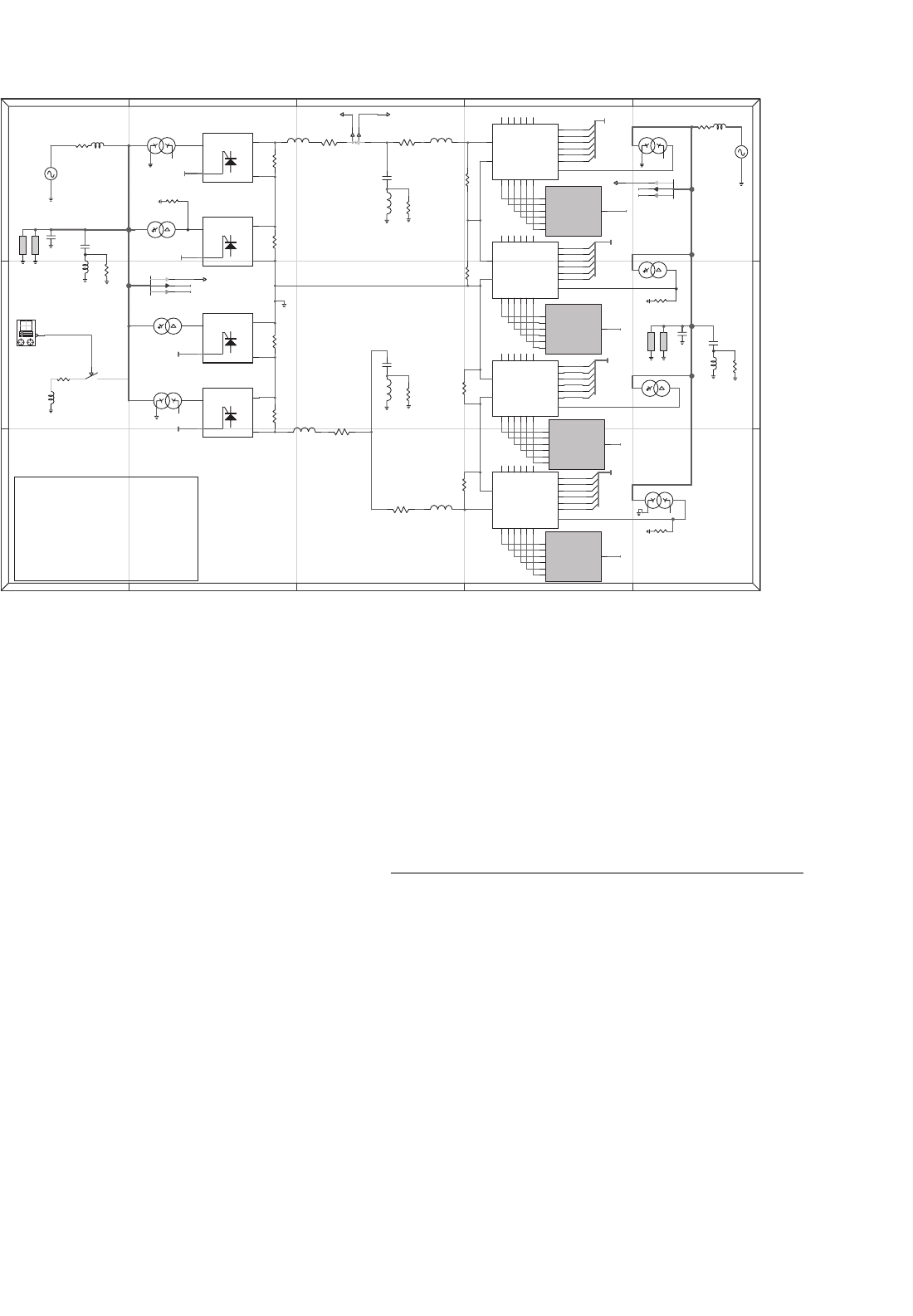
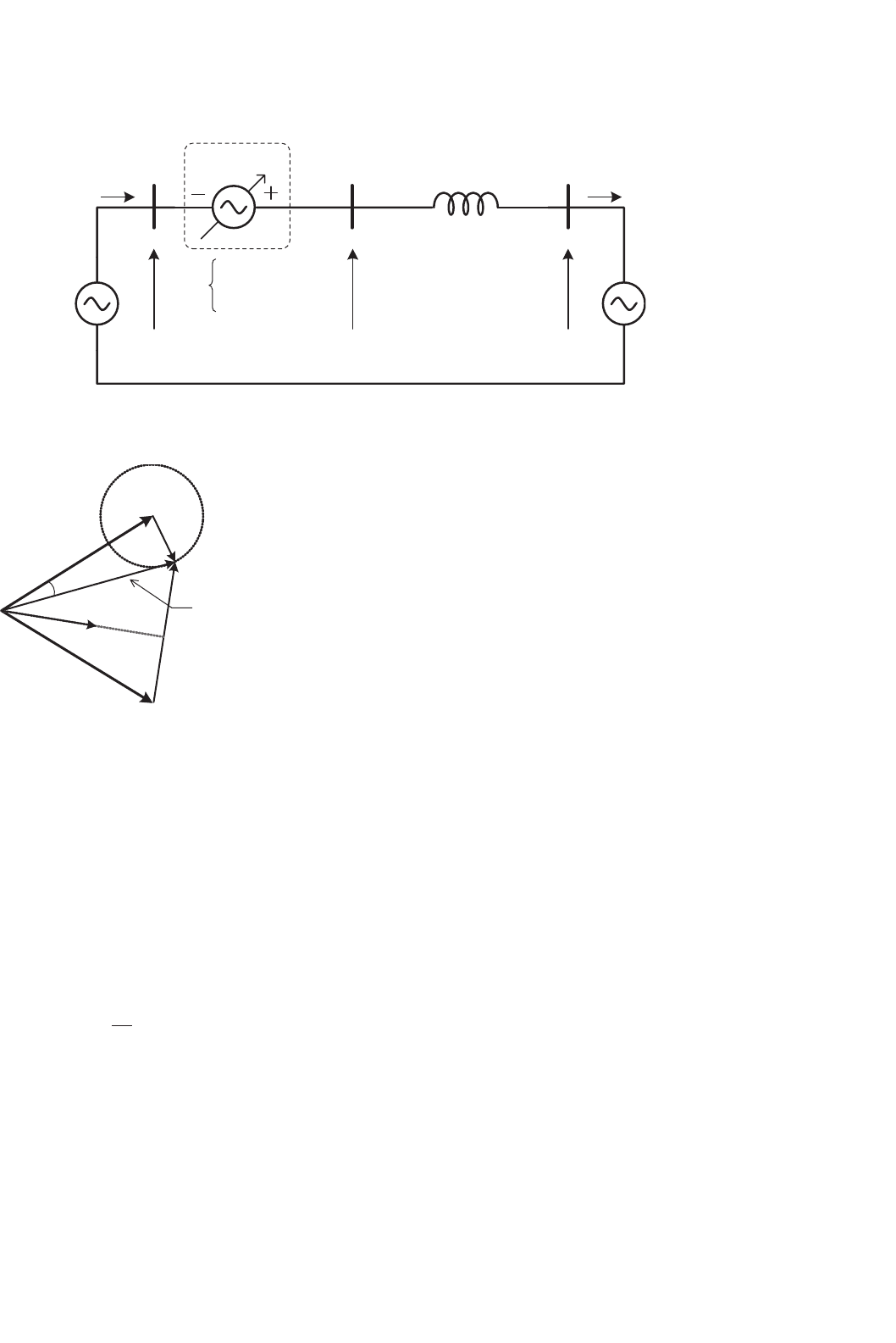
FIGURE 31.1 Ideal shunt compensator connected in the middle of a transmission line.
type [7]. On the other hand, the force commutated converters
using the self-commutated devices are basically of the voltage
source type. More details about current source and voltage
source converters can be found in many power electronics
text books, e.g. [3, 7].
31.2 Ideal Shunt Compensator
A simple and lossless AC system is composed of two ideal gen-
erators and a short transmission line, as shown in Fig. 31.1,
is considered as basis to the discussion of the operating prin-
ciples of a shunt compensator [8]. The transmission line is
modeled by an inductive reactance X
L
. In the circuit, a con-
tinuously controlled voltage source is connected in the middle
of the transmission line. It is assumed that the voltage phasors
V
S
and V
R
have the same magnitude and are phase-shifted
by δ. The subscript “S” stands for “Source” and “R” stands
for “Receptor.” Figure 31.2 shows the phasor diagram of the
system in Fig. 31.1, for the case in which the compensation
voltage phasor V
M
has also the same magnitude as V
S
and V
R
and its phase is exactly (−δ/2) with respect to V
S
and (+δ/2)
with respect to V
R
.
In this situation, the current I
SM
flows from the source
and the current I
MR
flows into the receptor. The phasor I
M
is the resulting current flowing through the ideal shunt com-
pensator, figure shows that this current I
M
, in this case, is
orthogonal to the voltage V
M
, which means that the ideal
shunt compensator voltage source does not have to gener-
ate or absorb active power and have only reactive power in its
terminals.
From Fig. 31.2 and knowing that no active power flows to
or from the ideal shunt compensator, it is possible to calculate
the power transferred from V
S
to V
R
which is given by:
P
S
=
2V
2
X
L
sin(δ/2) (31.1)
where, P
S
is the active power flowing from the source, V is the
magnitude of the voltages V
S
and V
R
.
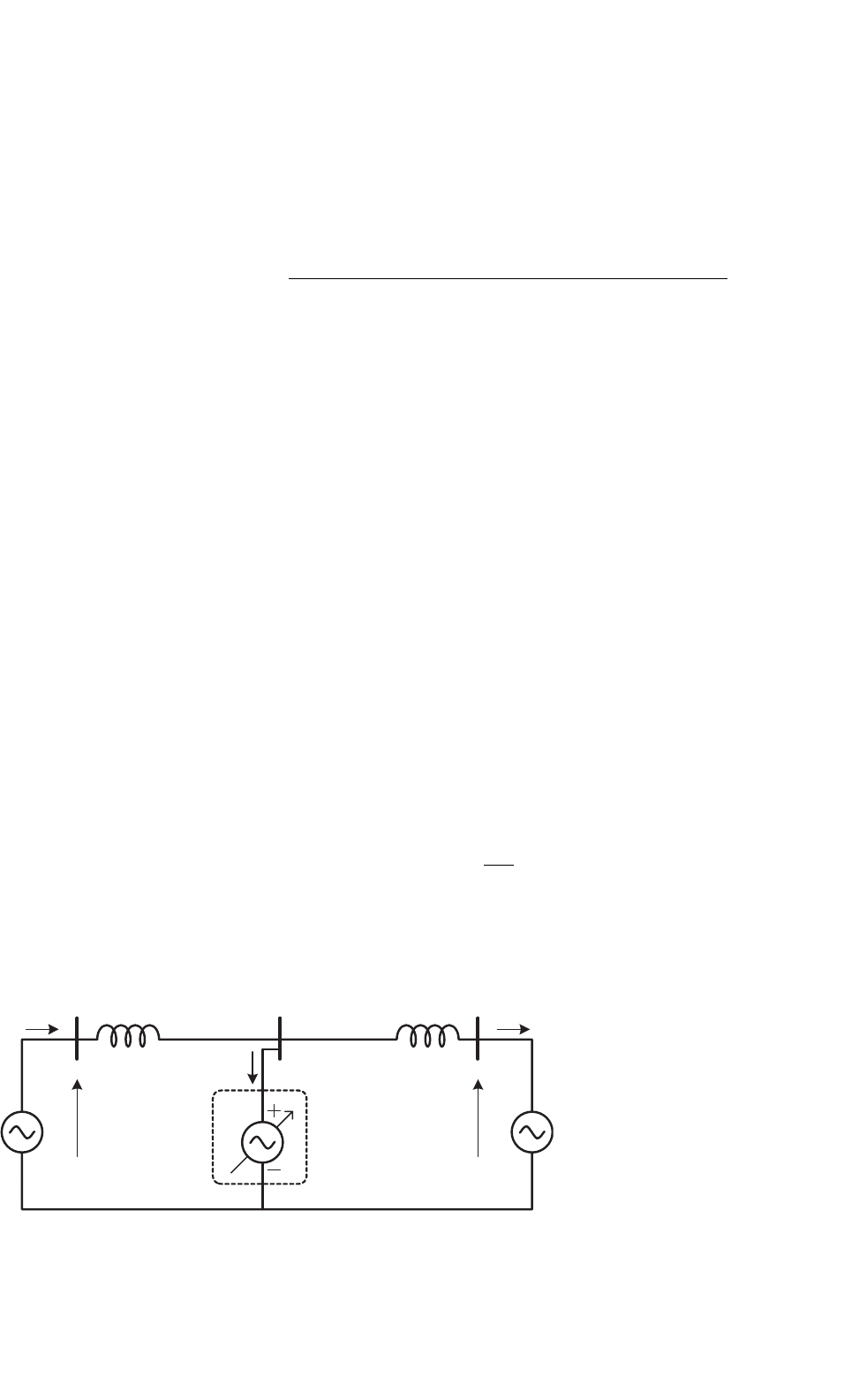
31 Flexible AC Transmission Systems 799
I
SM
V
M
O
V
R
= Ve
–jδ/2
V
S
= Ve
+jδ/2
j
(XL/2)I
SM
j
(XL/2)I
MR
I
MR
I
M
FIGURE 31.2 Phasor diagram of the system with shunt reactive power
compensation.
If the ideal shunt compensator were not present, the
transferred power would be given by:
P
S
=
V
2
X
L
sin δ (31.2)
Since 2 sin(δ/2) is always greater than sin δ for δ in the range
of [0, 2π], the ideal shunt compensator does improve the
power transfer capability of the transmission line. This voltage
source is in fact operating as an ideal reactive power shunt
compensator.
If the phase angle between V
M
and V
S
is different from δ/2
(as shown in Fig. 31.3), the power flowing through V
M
has
both active and reactive components.
With the characteristics of the ideal shunt compensator
presented above it is possible to synthesize power electronics-
based devices to operate as active or reactive power com-
pensators. This is discussed in the following sections. It will
be seen that the requirements of the device synthesis with
actual semiconductor switches for the situations of reactive
or active power compensation are different, due to the need of
V
c
I I
Ideal Series
Compensator
V
S
V
M1
V
M2
V
R
j
XL/2
j
XL/2
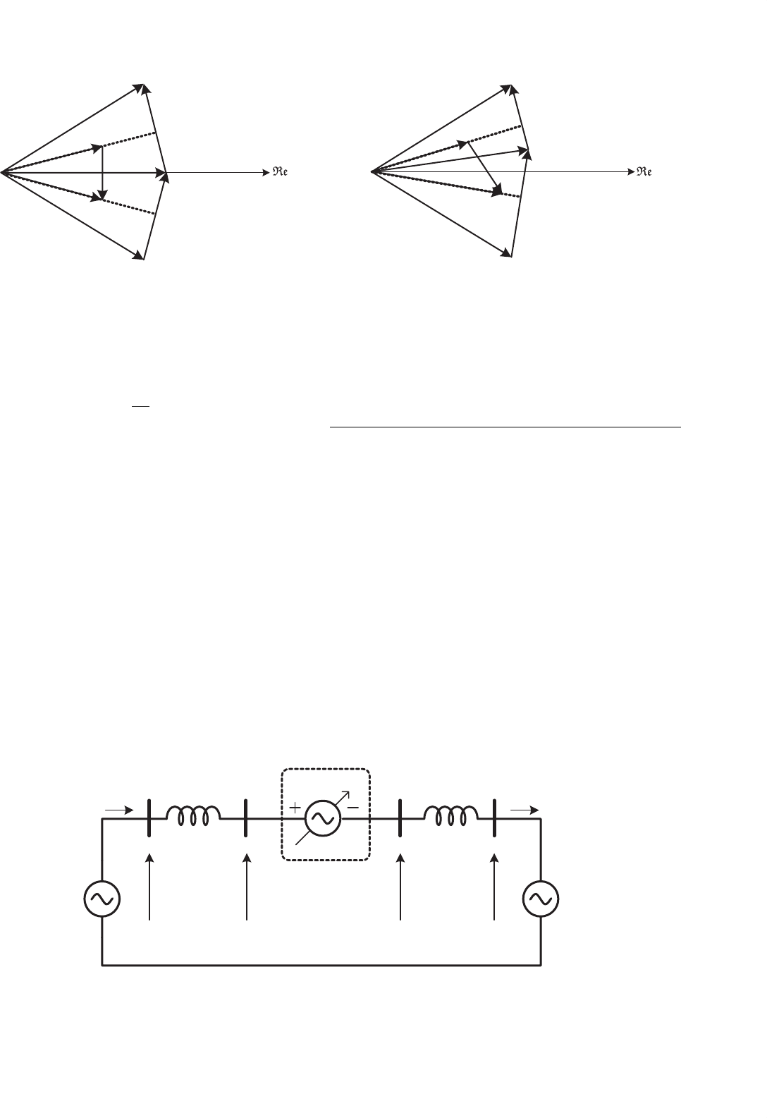
FIGURE 31.4 Ideal series compensator connected in the middle of a transmission line.
I
SM
V
M
O
I
MR
I
M
V
R
= Ve
–jδ/2
V
S
= Ve
+jδ/2
j
(XL/2)I
MR
j
(XL/2)I
SM
FIGURE 31.3 Phasor diagram of the system with shunt reactive and
active power compensation.
energy storage element or energy source if active power is to
be drained/generated by the shunt compensator.
31.3 Ideal Series Compensator
Similar to the previous section, the ideal series compensator is
modeled by a voltage source for which the phasor is V
C
, con-
nected in the middle of a lossless transmission line as shown
in Fig. 31.4.
The current flowing through the transmission line is
given by:
I = (V
SR
−V
C
)/jX
L
(31.3)
where V
SR
= V
S
−V
R
.
If the ideal series compensator voltage is generated in such
a way that its phasor V
C
is in quadrature with line current I,
this series compensator does not supply neither absorb active
power. As previously discussed, power at the series source is
only reactive and the voltage source may, in this particular case,
800 E. H. Watanabe et al.
be replaced by capacitive or inductive equivalent impedance.
The equivalent impedance would then given by
X
eq
= X
L
(1 +s) (31.4)
where,
s =
X
Comp
X
L
;(0≤
|
s
|
≤ 1) (31.5)
is the compensation factor and X
Comp
is the series equivalent
compensation reactance, negative if capacitive and positive if
inductive. In this case the compensation voltage is given by
V
C
= I
L
X
eq
(31.6)
and the transmitted power is equal to
P
s
=
V
2
X
L
(1 −s)
sin δ (31.7)
Equation (31.6) shows that the transmitted power can be
considerably increased by series compensation, choosing a
proper compensation factor s. The reactive power at the series
source is given by
Q
CS
=
2V
2
X
L
s
(1 −s)
2
(1 −cosδ) (31.8)
The left-hand side of Fig. 31.5a shows the phasor diagram
of the system in Fig. 31.4 without the ideal series compensator.
V
M2
V
M1
O
I
(a)
(b)
O
I
V
L
V
L
V
C
V
C
O
I
V
M2
O
I
V
M1
V
Z
/2
V
Z
/2
V
Z
/2
V
Z
/2
V
S
= V.e
+j /2
V
R
= V.e
–j /2
V
R
= V.e
–j /2
V
R
= V.e
–j /2
V
R
= V.e
–j /2
V
S
= V.e
+j /2
V
S
= V.e
+j /2
V
S
= V.e
+j /2
FIGURE 31.5 Phasor diagram of the series reactive compensator: (a) capacitive and (b) reactive mode.
The voltage phasor V
L
on the line reactance X
L
and the
compensator voltage phasor V
C
are shown for a given
compensation level, assuming that this voltage V
C
corresponds
to a capacitive compensation. In this case, the line current pha-
sor leads voltage phasor V
C
by 90
◦
and the total voltage drop
in the line V
Z
(=V
S
− V
R
− V
C
) is larger than the original
voltage drop V
L
. The current flowing in the line is larger after
compensation than before. This situation shows the case where
the series compensator is used to increase power flow.
The left-hand side of Fig. 31.5b shows the same non-
compensated situation as in the previous case. In the middle
is shown the case of inductive compensation. In this case, the
compensation voltage V
C
is in phase with the line drop volt-
age V
L
, producing an equivalent total voltage drop V
Z
smaller
than in the original case. As a result, the current phasor I
flowing in the line is smaller than before compensation. This
kind of compensation may be interesting in the case that the
power flowing through the line has to be decreased. In either
capacitive or inductive compensation modes, no active power
is absorbed or generated by the ideal series compensator.
Figure 31.6 shows an AC system with an ideal generic series
compensation voltage source V
C
for the general case where
it may not be in quadrature with the line current. In this
case, the compensator is able to fully control the phase dif-
ference between the two systems, thus controlling also the
active and reactive power exchanged between them. However,
in this case, the compensation source V
C
may have to absorb
or generate active power (P
C
), as well as to control the reactive
power (Q
C
).
Figure 31.7 shows the phasor diagram for the case of this
ideal generic series compensator. This figure shows also a
dashed-line circle with the locus of all the possible position
31 Flexible AC Transmission Systems 801
j XL
II
Ideal Generic
Series Compensator
V
S
V
R
V
S1
V
c
P
c
≠ 0
Q
c
≠ 0
FIGURE 31.6 Ideal generic series compensator.
I
O
α
V
c
j XL.I
V
R
= V.e
–j(δ – α)/2
V
SI
= V.e
+j(δ – α)/2
V
S
= V.e
+j(δ – α)/2
FIGURE 31.7 Phasor diagram of the AC system compensated with an
ideal generic series compensator.
that the compensation voltage V
C
could take, assuming that
the magnitude shown for this voltage is its maximum. Natu-
rally, if the sum of the compensation voltage and the source
voltage V
S
is on the circle, the magnitude of V
S1
may be smaller
or larger than the magnitude of V
S
.
If the compensation voltage V
C
added in series with V
S
produces a voltage V
S1
that has the same magnitude as V
S
but
is phase-shifted by an angle α, the power flowing through the
transmission line in Fig. 31.6 is given by:
P
S
=
V
2
X
L
sin (δ −α) (31.9)
Equation (31.8) shows that transmitted power increases as
the phase difference (δ − α) reaches 90
◦
. However, its maxi-
mum value is the same as in the case of no compensation. The
difference is that with this compensator the angle between
the two voltage sources at the terminals of the line can be
controlled.
In Fig. 31.7, voltage V
C
may have any phase angle with
respect to line current. Therefore, it may have to supply or
absorb active power, as well as control reactive power. As in
the case of the shunt device, this feature must also be taken
into account in the synthesis of the actual devices. As a first
approximation, when the goal is to control active power flow
through the transmission line, compensator location seems to
be just a question of convenience.
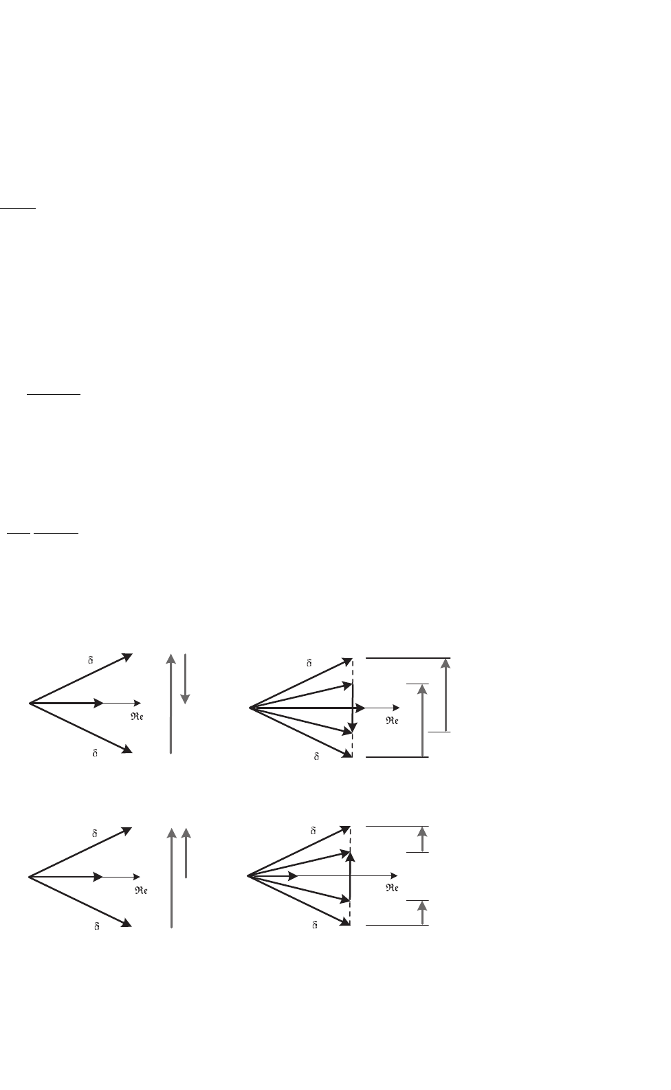
Figure 31.8 summarizes the active power transfer charac-
teristics in a transmission line as a function of the phase
difference δ between its sending and receiving ends, as shown
in Figs. 31.1 and 31.2, for the cases of the line without com-
pensation, line with series or shunt compensation, as well as
line with a phase-shift compensation. These characteristics are
drawn on the assumption that the source voltages V
S
and V
R
(see Fig. 31.2) have the same magnitude, which is a conven-
tional situation. A 50% series compensation (s =0.5 as defined
in Eq. (31.4) presents a significant increase in the line power
transfer capability.
In general, series compensation is the best choice for
increasing power transfer capability. The phase-shifter com-
pensator is important to connect two systems with excessive
or uncontrollable phase difference. It does not increase power
transfer capability significantly; however, it may allow the
adjustment of large or highly variable phase differences. The
shunt compensator does not increase power transfer capabil-
ity in a significant way in its normal operating region, where
the angle δ is naturally below 90
◦
and in general around 30
◦
.
The great importance of the shunt compensator is the increase
in the stability margin, as explained in Fig. 31.9.
Figure 31.9 shows the power transfer P
δ
characteristics of
a transmission line, which is first assumed to be transmitting
power P
S0
at phase angle δ
0
. If a problem happens in the
line (a fault, for example) the turbine that drives the generator
cannot change its input mechanical power immediately even if
there is no power transmission for a short time. This situation
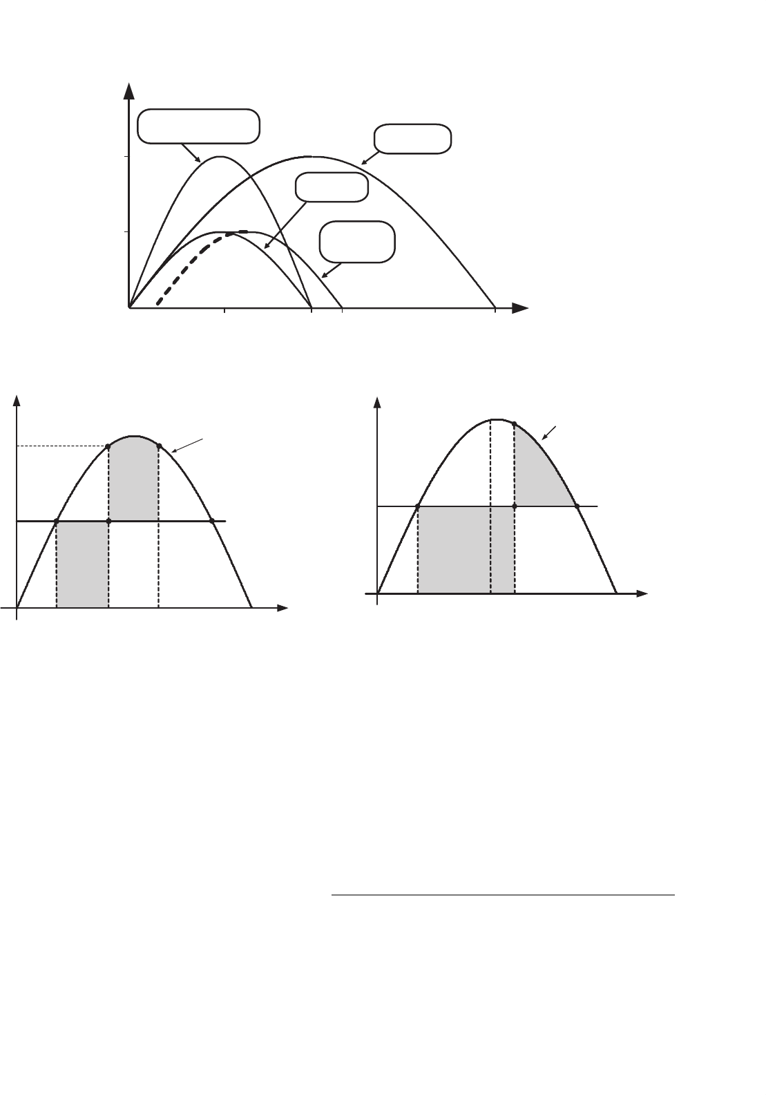
802 E. H. Watanabe et al.
P
s
(pu)
δ (rad)
2
1
0
π /2 π + α 2 π
With shunt
compensation
With phase
shifter
compensation
Without
compensation
With 50% of series
capacitive compensation
π
FIGURE 31.8 Power transfer characteristics for the case of shunt, series, and no compensation.
P
s0
C
A
B
D
P
s
P
s1
A
1
A
3
A
2
P
δ
0
δ
1
δδ
0
δ
2
FIGURE 31.9 Stability margin characteristics – stable situation.
accelerates the generator, increasing its frequency and leading
to an increase of the phase angle δ to δ
1
. If the line restarts
operation at the instant corresponding to this phase angle δ
1
,
the transmitted power will be P
1
, which is larger than P
0
and
decelerates the turbine/generator. The area A
1
corresponds to
the energy that accelerated the turbine. As the frequency gets
higher than the rated frequency at (P
S1
, δ
1
), the phase angle
will increase up to δ
2
, where the area A
2
is equal to the area A
1
.
If the area given by the A
2
plus A
3
is larger than A
1
, the system
is said to be dynamically stable. On the contrary, if it is not
possible to have an area A
2
equal to A
1
, the system is said to be
unstable. An unstable situation is shown in Fig. 31.10, where
the system is the same as in Fig. 31.9 but with a longer interval
with no power transmission. In this case, the turbine/generator
accelerates more than in the case in Fig. 31.9 and the phase
angle δ goes over its critical value δ
c
reaching δ
1
. Therefore,
the area below the P
δ
curve to decelerate the system is not
P
s0
AB
C
D
P
s
δ
c
δ
0
A
1
A
2
δ
1
P
δ
0
δ
FIGURE 31.10 Stability margin characteristics – unstable situation.
enough leading to an unstable system because A
2
is smaller
than A
1
.
Looking at Fig. 31.8 it is possible to see that, depending on
the operating point, all three compensation methods increase
the stability margin as the area under the curve of transmitted
power P
δ
versus phase angle δ is increased. However, the ideal
shunt compensator is the one that most increases this area, this
is the reason why it is said to be the best option to increase the
stability margin.
31.4 Synthesis of FACTS Devices
It has been stated that the synthesis of the compensators
presented in Sections 31.2 and 31.3 may be achieved with
thyristors or self-commutated switches like GTO, IGBT, or
IGCT. Each type of switches leads to devices with different
31 Flexible AC Transmission Systems 803
operating principles and synthesis concepts, and that is a
reason why they should be discussed separately. Terms and
definitions for most of the FACTS devices are given in [9].
Thyristor-based FACTS devices use line or natural commu-
tation together with large energy storage elements (capacitors
or reactors). On the other hand, devices based on self-
commutating switches like GTOs, IGCTs, or IGBTs uses
gate-controlled commutation. In general, it is said that the
first generation of FACTS devices is based on conventional
line commutated thyristors and the subsequent generations are
based on gate-controlled devices. The most important FACTS
devices based on thyristors and self-commutating devices are
presented in the next sections.
31.4.1 Thyristor-based FACTS Devices
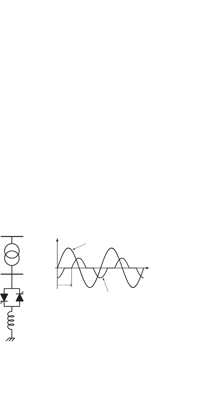
31.4.1.1 Thyristor-controlled Reactor
The most used thyristor-based FACTS device is the thyristor-
controlled reactor (TCR) shown in Fig. 31.11a. This is a shunt
compensator which produces an equivalent continuous vari-
able inductive reactance by using phase-angle control. Figure
31.11b shows the voltage and current waveforms of the TCR.
The current is controlled by the firing-angle α – its fundamen-
tal component can be larger or smaller depending on the angle
α which may vary from 90 to 180
◦
, measured from the zero-
crossing of the voltage. At α =90
◦
, the reactor is fully inserted
in the circuit and for α =180
◦
, the reactor is completely out
of the circuit. Figure 31.12 shows the equivalent admittance
of the TCR as function of the firing-angle α. Naturally, this
admittance is always inductive.
AC
System
Th
1
Th
2
Transformer
L
(a) (b)
Voltage on the TCR
Reactor current, i
L
0
1
α
–1
FIGURE 31.11 (a) TCR and (b) its voltage and current waveforms.
31.4.1.2 Thyristor-switched Capacitor
Figure 31.13 shows the thyristor-switched capacitor (TSC). In
this device the word “controlled” used in the case of the reactor
is substituted by “switched,” because the thyristor is turned-on
only when zero-voltage switching (ZVS) condition is achieved.
This means that the voltage across the thyristor terminals has
to be zero at the turn-on instant. In practical cases, it may be
slightly positive, since thyristors need positive anode–cathode
voltages to be triggered (large anode–cathode voltage during
turn-on, however, may produce a large current spike that may
damage the thyristors). Therefore, due to this switching char-
acteristic, the thyristors can only connect the capacitor to the
grid or disconnect it. Consequently, only step-like control is
possible and, therefore, a continuous control is not possible.
The capacitor connection to or disconnection from the grid
is normally done at very low frequencies and the harmonics,
when they appear, are not a serious concern.
31.4.1.3 Static Var Compensator
The use of the TCR shown in Fig. 31.11 or the TSC shown
in Fig. 31.13 allows only continuous inductive compensation
or capacitive discontinuous compensation. However, in most
applications, it is desirable to have continuous capacitive or
inductive compensation. The static var compensator (SVC) is
generally designed to operate in both inductive and capacitive
continuous compensation [10, 11]. The TCR serves as the con-
troller basis for the conventional SVC used for reactive power
compensation, for either voltage regulation or power factor
correction.
Figure 31.14 shows a single-line diagram of a SVC, where
the TCRs are connected and the capacitors are Y connected.
804 E. H. Watanabe et al.
135
Y
L
(α) (pu)
90
180
Firing angle, α (degrees)
0
1
FIGURE 31.12 Equivalent admittance of a TCR as function of the firing-angle α.
C
AC
System
Th
2
Th
1
Transformer
FIGURE 31.13 Thyristor-switched capacitor.
The circuit does not show the filters that are normally needed
due to the switching-generated harmonics. In some cases, the
fixed capacitor can be replaced by a TSC to get more flexibility
in terms of control range.
The capacitor of the SVC is calculated in such a way as to
generate the maximum capacitive reactive power that it has
to control. This condition is achieved when the thyristors are
turned-off (α = 180
◦
). On the other hand, the TCR inductor
maximum reactive power has to be greater than the reactive
power of the capacitor bank. In this way, the SVC is able
to control the reactive power from capacitive to inductive.
The maximum inductive reactive power is given for the case
when the thyristors are turned-on at minimum firing-angle
(α = 90
◦
). Thus, the SVC can control reactive power from
maximum capacitive for α = 180
◦
to maximum inductive for
α = 90
◦
. In this sense, the SVC represents an adjustable funda-
mental frequency susceptance to the AC network, controlled
by the firing-angle of the TCR thyristors (90
◦
<α<180
◦
).
The SVC is well-known and many examples of successful
applications can be found around the world.
Due to the once-per-cycle thyristor firing with phase-
angle control, current with low-order harmonic components
appears and Y– transformers and passive filters may be
needed to eliminate them. Three sets of TCRs connected in
the side of Y– transformers form a conventional 6-pulse
TCR. To minimize harmonic generation, it is common to have
two sets of transformers connected in Y– and – with the
TCR connected in the side forming a 12-pulse TCR.
31.4.1.4 Thyristor-switched Series Capacitor
Figure 31.15 shows the thyristor-switched series capacitor
(TSSC). In this device, the thyristors should be kept untrig-
gered so as to connect the capacitors in series with the
transmission line. If the thyristors are turned-on, the capaci-
tor is bypassed. Thyristors turn-on must be at a zero-voltage
condition (ZVS), as it occurs in the case of the TSC, to avoid
current spikes in the switches. An example of an application
based on this concept is presented in [12].
This compensation system has the advantage of being very
simple. However, it does not allow continuous control. If the
connection/disconnection of the capacitors is to be made at
sporadic switching, no harmonic problem occurs. Depending
on the frequency the thyristors are switched, harmonic or sub-
harmonics may appear. In this arrangement, it is interesting
to choose the value of the capacitors in such a way that many
different combinations can be achieved. For example, if the