Power electronic handbook
Подождите немного. Документ загружается.

22 Electronic Ballasts 571
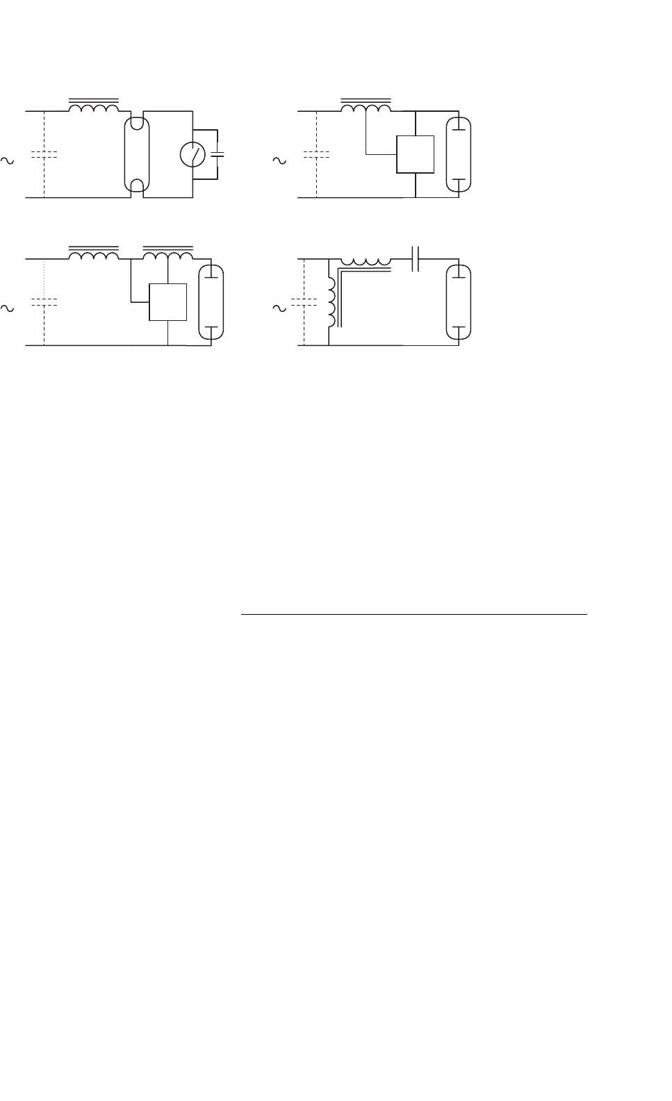
Line
Glow
Switch
(a)
Line
Starter
(b)
Line
Starter
(c)
Ballast Ballast
Ballast Starting Transformer
Line
(d)
CWA
Air Gapped
Core
FIGURE 22.8 Typical electromagnetic ballast used to supply discharge lamps at low frequency.
inductive ballast, the CWA also exhibits higher input power
factor, lower line extinguishing voltage and lower line starting
currents.
The main advantage of electromagnetic ballasts is their
simplicity, which in turn provides low cost and high reliabil-
ity. However, since they operate at line frequencies, typically
50–60 Hz, they also feature high size and weight. Other
important drawbacks of electromagnetic ballasts are as follows:
•
Low efficiency, especially for those ballasts featuring good
lamp power regulation against line voltage variation.
• Low reliability for ignition and re-ignition. If the voltage
spike is not well located within the line period the ignition
of the lamp can fail.
• Difficult to control the lamp luminous flux (dimming).
• Lamp operating point changes due to lamp aging process,
thus reducing lamp life.
• Low input power factor and high harmonic distortion.
Large capacitors are needed across the line input to
increase power factor.
• Over-current risk due to ballast saturation caused by rec-
tifying effect of some discharge lamps, specially at the end
of their life.
• Flickering and stroboscopic effect due to low frequency
supply. The energy radiated by the lamp is a function
of the instantaneous input power. Therefore, when sup-
plied from an AC line an instantaneous variation of
the light output occurs, which is called flicker. For a
line frequency of 60 Hz the resulting light frequency
is 120 Hz. This variation is too fast for the human
eye, but when rapidly moving objects are viewed under
these lamps, the objects seem to move slowly or even
halted. This is called stroboscopic effect, and can be very
dangerous in industrial environments. A flicker index
is defined with values from 0 to 1.0 [1]. The higher
the flicker index, higher is the possibilities of noticeable
stroboscopic effect.
• Unsuitable for DC applications (emergency lighting,
automobile lighting, etc.).
22.2 High Frequency Supply of
Discharge Lamps
22.2.1 General Block Diagram of Electronic
Ballasts
Figure 22.9 shows the general block diagram of a typical
electronic ballast. The main stages are the following:
• EMI filter. This filter is mandatory for commercial elec-
tronic ballast. Usually it consists of two coupled inductors
and a capacitor. The input filter is used to attenuate
the electro magnetic interference (EMI) generated by the
high frequency stages of the ballasts. It also protects the
ballast against possible line transients.
• AC–DC converter. This stage is used to generate a DC
voltage level from the AC line. Normally a full-bridge
diode rectifier followed by a filter capacitor is used.
However, this simple rectifier provides low input power
factor and poor voltage regulation. In order to obtain
a higher power factor and a regulated bus voltage, active
converters can be used as expounded later in this chapter.
• DC–AC inverter and high frequency ballast. These stages
are used to supply the lamp at high frequency. The
inverter generates a high frequency waveform and the

572 J. M. Alonso
EMI
FILTER
POWER
LINE
AC-DC
CONVERTER
DC
BUS
DC-AC
CONVERTER
(H.F.)
H. F.
BALLAST
LAMP
CONTROL & PROTECTION
CIRCUIT
STARTING
CIRCUIT
FIGURE 22.9 Block diagram of a typical electronic ballast.
ballast is used to limit the current through the discharge.
Both inductors or capacitors can be used to perform
this function, with the advantage of low size and weight,
because they operate at high frequencies.
• Starting circuit. In most electronic ballast, specially those
for low-pressure discharge lamps, the high frequency bal-
last is used to both ignite the lamp and limit the lamp
current at steady state. Therefore, no extra starting cir-
cuit is necessary. However, when supplying high pressure
discharge lamps, the starting voltages are quite higher
and separate ignition circuits are needed, specially if hot
re-ignition is pursued.
• Control and protection circuit. This stage includes the
main oscillator, error amplifiers to regulate lamp current
or power, output over-voltage protection, timers to con-
trol the ignition times, over-current protection, lamp fail-
ure protection, etc. It can vary from very simple circuits,
those used in self-oscillating ballasts, to very complicated
ones, which sometimes include a microprocessor-based
control circuit.
There are several important topics when designing elec-
tronic ballasts:
•
Operating frequency. The operating frequency should be
high in order to take benefit of the lower size and weight
of the reactive elements used to stabilize the discharge.
Usually, the operating frequency should be higher than
20 kHz to avoid audible frequencies, which can produce
annoying noises. On the other hand, a higher frequency
produces higher switching losses and a practical limit of
the switching frequency is about 100 kHz when using
MOSFET switches. It is also important to avoid frequen-
cies in the range 30–40 kHz, because these frequencies are
normally used in IR remote controls and could generate
some kind of interference.
• Lamp current waveform. In order to attain the maximum
lamp life, it is important to drive the lamp with symmet-
rical alternating currents, thus making use of both the
lamp electrodes alternately. Also, an important parame-
ter is the lamp current crest factor (CF), which is the ratio
of the peak value to the rms value of the lamp current.
In case of electronic ballasts, the peak value of the low
frequency modulated envelope to the rms value should
be used. The higher the CF, the lower the lamp life. The
ideal situation is to supply the lamp with a pure sinusoidal
waveform. Usually, a CF lower than 1.7 is recommend to
avoid early aging of the lamp.
• Lamp starting procedure. This is a very important issue
when developing commercially available electronic bal-
lasts. The reason is that the life of the lamp greatly
depends on how well the lamp starting is performed,
specially for hot-cathode fluorescent lamps. During the
starting process, electrodes must be warmed up to the
emission temperature, about 800
◦
C, and no high volt-
age should be applied until their temperature is suffi-
ciently high, thus avoiding sputtering damage. Once the
electrodes reach the emission temperature, the starting
voltage can be applied to ignite the lamp. For lamps with
cold cathodes, the starting voltage must be applied rapidly
to prevent harmful glow discharge and cathode sputter-
ing. In any case, starting voltage must be limited to the
minimum value to ignite the lamp, since higher volt-
ages could provide undesirable starting conditions which
would reduce the life of the lamp.
• Dimming. This is an important feature which allows the
ballast to control lamp power and thereby lighting out-
put. Usually the switching frequency is used in solid-state
ballasts as a control parameter to provide dimming capa-
bility. Variations in frequency affect the high frequency
ballast impedance and allow to change the discharge cur-
rent. For example, if an inductor is used as high frequency
ballast, a frequency increase yields an increase in the bal-
last impedance, thus decreasing lamp current. Dimming
should be carried out smoothly, avoiding abrupt changes
in lamp power when passing from one level to another. In
an eventual power cutoff, the lamp should be re-started
22 Electronic Ballasts 573
at maximum lighting level and then slowly reduced to
the required output level.
• Acoustic resonance. The HID lamps exhibit an unsta-
ble operation when they are supplied at high frequency.
At a certain operating frequencies the arc fluctuates and
becomes unstable, what can be observed as a high flicker
due to important changes in the lamp power and thus in
the lighting output. This can be explained by the depen-
dence of the damping of acoustic waves on the plasma
composition and pressure. More information about this
topic can be found in [2]. The avoidance of acoustic
resonance is mandatory to implement commercial elec-
tronic ballasts. This can be performed by selecting the
operating frequency in a range free of acoustic reso-
nances, typically below 1 kHz and over 100 kHz. Other
methods are frequency modulation, square wave opera-
tion and sine-wave superposed with the third harmonic
frequency [3, 4].
22.2.2 Classification of Electronic Ballast
Topologies
Typical topologies used to supply discharge lamps at high fre-
quency can be classified into two main groups: non-resonant
ballasts and resonant ballasts.
22.2.2.1 Non-resonant Ballasts
These topologies are usually obtained by removing the output
diode of DC-to-DC converters, in order to supply alternat-
ing current to the lamp. Current mode control is normally
employed to limit the discharge lamp current. The lamp is
supplied with a square current waveform, which can exhibit a
DC level in some cases. A small capacitor is used to initially
ignite the lamp, but its effect at steady-state operation can be
neglected.
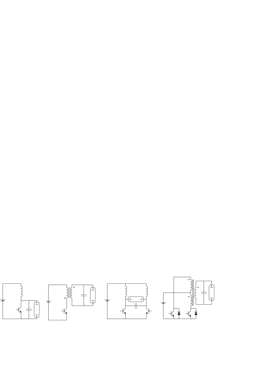
Examples of non-resonant electronic ballasts are shown
in Fig. 22.10. Figure 22.10a, illustrates a boost-based and a
flyback-based ballasts, respectively. Other topologies, which
can supply symmetric alternating current through the lamp,
V
in
V
in
V
in
V
in
L
Q1
D1
Q1
Q1
Q2
Q2
D1 D2
Lamp
(d)(c)(b)(a)
C1
L1 L2
Q1
C
C
C
Lamp
Lamp
Lamp
FIGURE 22.10 Non-resonant electronic ballasts.
are shown in Fig. 22.10c (symmetric boost) and 22.10d
(push–pull).
These topologies present several drawbacks such as high-
voltage spikes across the switch, which necessitates the use of
high voltage transistors, and high switching losses due to hard
switching, which gives low efficiency specially for high powers.
Besides, since the ideal situation is the lamp being supplied
with a sine wave, these circuits produce an early aging of the
lamp. To conclude, typical applications of these topologies are
portable and emergency equipment, where lamp power is low
and the number of ignitions during its life is not very high.
Some applications of these circuits can be found in [5–8].
22.2.2.2 Resonant Ballasts
These ballasts use a resonant tank circuit to supply the lamp.
The resonant tank filters the high order harmonics, thus
obtaining a sine current waveform through the lamp. Resonant
ballasts can be classified into two categories:
A. Current-fed resonant ballasts
These ballasts are supplied with a DC current source, usu-
ally obtained by means of a choke inductor in series with the
input DC voltage source. The DC current is transformed into
an alternating square current waveform by switching power
transitors. Typical topologies of this type of ballasts are shown
in Fig. 22.11.
The topology shown in Fig. 22.11a corresponds to a class E
inverter. Inductor Le is used to obtain a DC input current
with low current ripple. This current supplies the resonant
tank through the power switch formed by Q1–D1. The reso-
nant tank used in this topology can vary from one ballast to
another; the circuit shown in Fig. 22.11a is one which is nor-
mally used. The main advantage of this topology is that zero
voltage switching (ZVS) can be attained in the power switch,
thus reducing the switching losses and making possible the
operation at very high frequencies, which can reach several
megahertz. This allows to drastically reduce the size and weight
of the ballast. However, the adjustment of the circuit parame-
ters to obtain the optimum operation results is quite difficult,
specially for mass production. Another important drawback
is the high voltage stress across the switch, which can reach
574 J. M. Alonso
(a)
V
in
Le
Q1
Lamp
D1
L1
C1
C2
C
Le
Lamp
V
in
(b)
Q1 Q2
(c)
C
Le
L1
L1
L2
L
Lamp
V
in
FIGURE 22.11 Two typical current-fed resonant inverters: (a) class E inverter; (b) current-fed push–pull inverter; and (c) current-fed full-bridge
resonant inverter.
values of three times the DC input voltage. For these reasons,
the main applications of this circuit are battery supply ballasts
with low input voltage and low lamp power, as those used
in emergency lighting and portable equipment. Typical power
range of this ballast varies from 5 to 30 W. Applications of this
circuit can be found in [9, 10].
Another typical topology in this group is the current-fed
push-pull inverter shown in Fig. 22.11b. In this circuit, a DC
input current is obtained by means of choke inductor Le. Tran-
sistors are operated with a 50% duty cycle, thus providing a
current square wave, which supplies the current-fed parallel
resonant circuit formed by the mutual inductance of the trans-
former and capacitor C. This circuit has the advantage of being
relatively easy to implement in a self-oscillating configuration,
avoiding the use of extra control circuits and thereby reducing
the cost. Also, ZVS can be obtained in the power switches.
However, the switches also present a high voltage stress, about
three times the DC input voltage, which makes this topology
unsuitable for power line applications. This circuit is also nor-
mally used in battery-operated applications in a self-oscillating
arrangement. The typical power range is 4–100W. Applications
based on this circuit can be found in [11, 12].
Finally, Fig. 22.11c shows a current fed full-bridge resonant
inverter, which can be used for higher power rating. Also,
this circuit allows to control the output power at constant
frequency by switching the devices of the same leg simulta-
neously, generating a quasi-square current wave through the
resonant tank [13].
B. Voltage-fed resonant ballasts
At present, electronic ballast manufactures mostly use voltage-
fed resonant ballasts, specially for applications supplied from
the AC mains. The circuit is fed from a DC voltage source,
normally obtained by line voltage rectifying. A square wave
voltage waveform is then obtained by switching the transis-
tors with a 50% duty cycle, and used to feed a series resonant
circuit. This resonant tank filters the high/order harmonics
and supplies the lamp with a sine current waveform. One
advantage of the voltage-fed series resonant circuit is that the
starting voltage can be easily obtained without using extra igni-
tion capacitors by operating close to resonant tank frequency.
Figure 22.12 shows electrical diagrams of typical voltage-fed
resonant ballasts.
The voltage-fed version of the push–pull inverter is illus-
trated in Fig. 22.12a. This inverter includes a transformer,
which can be used to step up or down the input voltage in
order to obtain an adequate rms value of the output square
wave voltage. This provides higher design flexibility but also
increases the cost. One disadvantage is that the voltage across
transistors is twice the input voltage, what can be quite high for
line applications. Therefore, this inverter is normally used for
low voltage applications. Another important drawback of this
voltage-fed inverter is that any asymmetry in the two primary
windings (different number of turns) or in the switching times
of power transistors would provide an undesirable DC level in
the transformer magnetic flux, which in turn could saturate
the core or decrease the efficiency due to the circulation of DC
currents.
Figure 22.12b and 22.12c illustrates two possible arrange-
ments for the voltage-fed half-bridge resonant inverter. The
former is normally referred as asymmetric half-bridge, and
uses one of the resonant tank capacitors (C1 in the figure) to
block the DC voltage level of the square wave generated by
the bridge. This means that capacitor C1 will exhibit a DC
level equal to half the DC input voltage superimposed to its
normal alternating voltage. A transformer can also be used
in this inverter to step up or down the input voltage to the
required level for each application. In this case, the use of the
series capacitor C1 prevents from any DC current circulating
through the primary winding, thus avoiding transformer sat-
uration. This topology is widely used by ballast manufacturers
to supply fluorescent lamps, especially in the self-oscillating
version which allows to drastically reduce the cost. When
supplying hot cathode fluorescent lamps, the parallel capac-
itor C2 is normally placed across two electrodes, as shown in
Fig. 22.12b, in order to provide a preheating current for the
electrodes and achieve soft ignition. Figure 22.12c shows other
version of the half-bridge topology, using two bulk capacitors
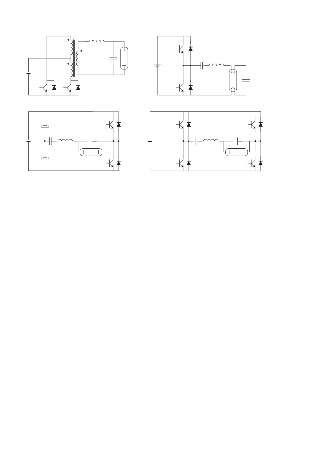
22 Electronic Ballasts 575
(a)
C1
L1
Lamp
V
in
(b)
Q1
Q2
D1 D2
Q1
D1
Q2
D2
C1
C2
L1
Lamp
V
in
(c)
Q1
Q2
D2
C1
+
+
C2
L1
V
in
C3
C4
D1
Q1
Q3
D3
D1
V
in
Q4
Q2
D2
D4
C1 C2L1
Lamp
(d)
FIGURE 22.12 Typical voltage-fed resonant inverters: (a) push–pull; (b)–(c) half-bridge; and (d) full-bridge.
to provide a floating voltage level equal to half the input volt-
age. In this case, capacitor C1 is no longer used to block a DC
voltage, thus showing lower voltage stress.
Finally, for the high power range (>200 W) the full-bridge
topology shown in Fig. 22.12d is normally used. The transis-
tors of each half-bridge are operated with a 50% duty cycle and
their switching signals are phase-shifted by 180
◦
. Thus, when
switches Q1 and Q2 are activated, direct voltage V
in
is applied
to the resonant tank, and when switches Q3 and Q4 are acti-
vated, the reverse voltage −V
in
is obtained across the resonant
circuit. One of the advantages of this circuit is that the switch-
ing signals of the two branches can be phase-shifted by angles
between 0 and 180
◦
, thus controlling the rms voltage applied
to the resonant tank ranging from 0 to V
in
. This provides an
additional parameter to control the output power at constant
frequency, the results are useful to implement dimming ballast.
22.3 Discharge Lamp Modeling
The low frequency of the mains is not an adequate power
source for supplying discharge lamps. At these low frequencies,
electrons and ionized atoms have enough time to recombine
at each current reversal. For this reason, the discharge must be
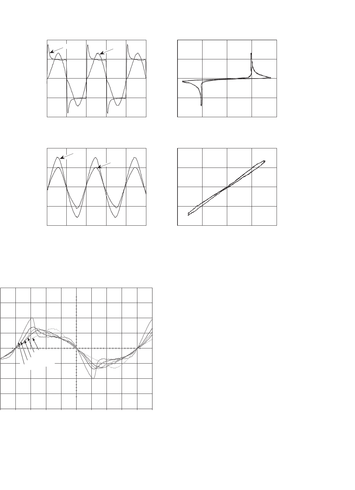
re-ignited twice within each line period. Figure 22.13a illus-
trates the current and voltage waveforms and the I–V char-
acteristics of a 150 W HPS lamp operated with an inductive
ballast at 50 Hz. As can be seen, the re-ignition voltage spike
is nearly 50% higher than the normal discharge voltage, which
is constant during the rest of the half-cycle.
When lamps are operated at higher frequencies (above
5 kHz), electrons and ions do not have enough time to recom-
bine. Therefore, charge carrier density is sufficiently high at
each current reversal and no extra power is needed to re-ignite
the lamp. The result is an increase in the luminous flux com-
pared to that at low frequencies, which is especially high for
fluorescent lamps (10–15%).
Figure 22.13b shows the lamp waveforms and I–V charac-
teristics for the same 150 W HPS when supplied at 50 kHz. It
is shown how the re-ignition voltage spikes disappear and the
lamp behavior is nearly resistive.
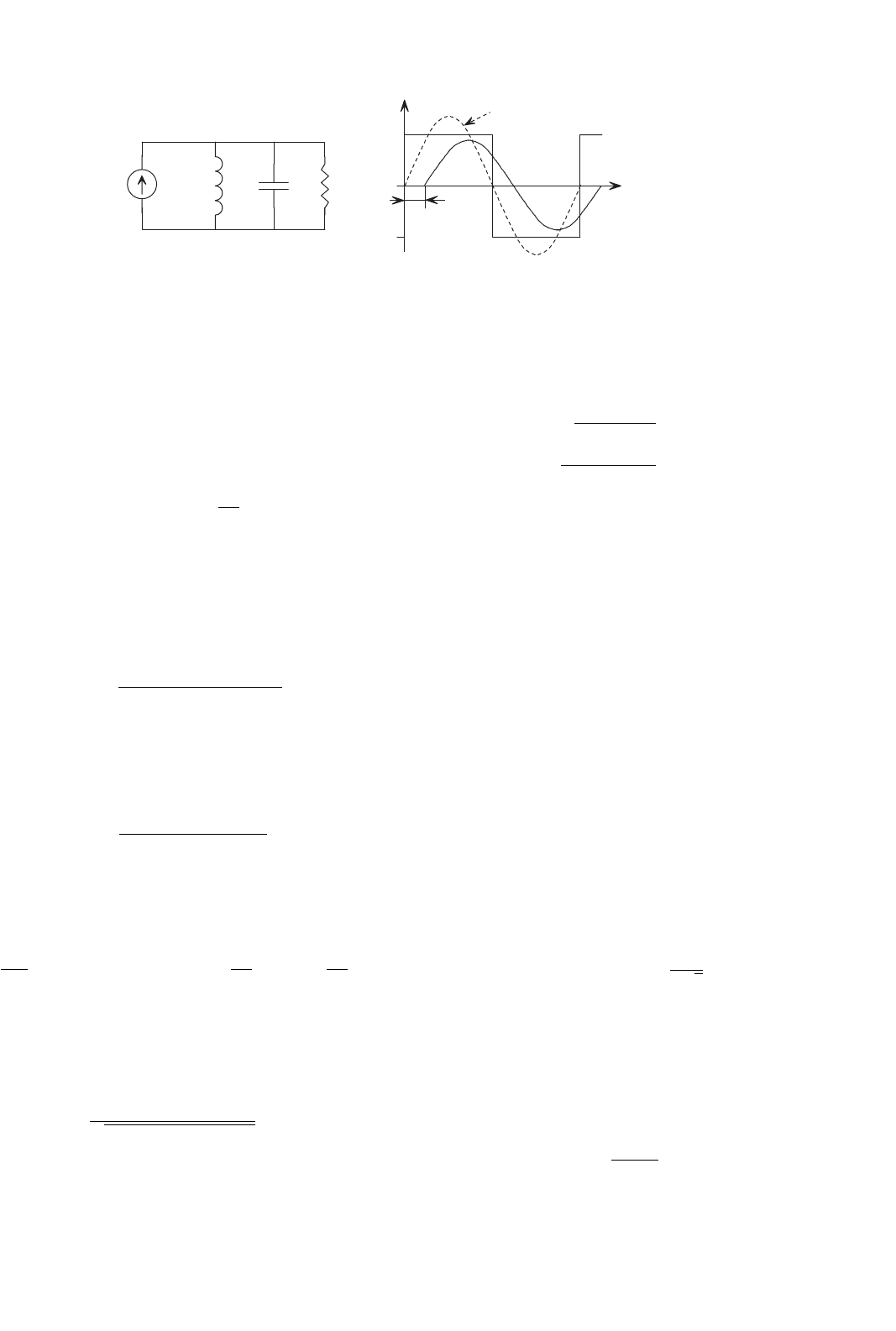
Figure 22.14 illustrates how the voltage waveforms change
in a fluorescent lamp when increasing the supply frequency.
As can be seen, at a frequency of 1 kHz, the voltage is already
nearly sinusoidal and the lamp exhibits a resistive behavior.
Therefore, a resistor can be used to model the lamp at high
frequencies for ballast design purposes. However, most lamp
manufactures provide only lamp data for operating at low fre-
quencies, where the lamp behaves as a square wave voltage
source. Table 22.2 shows the low frequency electric data of
different discharge lamps provided by the manufacturer and
the measured values at high frequency for the same lamps. As
can be seen, a power factor close to unity is obtained at high
frequency.
The equivalent lamp resistance at high frequencies can be
easily estimated from the low frequency data. Lamp power at
576 J. M. Alonso
0 0.01 0.02 0.03 0.04 0.05
−200
−100
0
100
200
(V)
(A)
t (s)
−4
4
−2
2
Vla
Ila
0 100 200
−4
−2
0
2
4
Ila (A)
Vla (V)
0
(a)
0 10
−200
−100
0
100
200
t (µs)
Vla
Ila
(A)
−4
4
−2
2
0
20 30 40 50
(V)
−200 −100
0 100 200
−3
−1.5
0
1.5
3
Ila (A)
Vla (V)
(b)
−200 −100
FIGURE 22.13 150 W HPS lamp waveforms and I–V characteristics at: (a) 50 Hz and (b) 50 kHz.
100
200
500
1000
25000
Frequency
(Hz)
FIGURE 22.14 Voltage waveforms for a 36 W linear fluorescent lamp
supplied through a resistive ballast at nominal power and different
operating frequencies. Vertical scale: 100 V/DIV.
any operating frequency can be expressed as follows:
P
LA
= V
LA
I
LA
FP
LA
(22.2)
where V
LA
and I
LA
are the rms values of lamp voltage and
current, and FP
LA
is the lamp power factor.
At line frequencies, the lamp power factor is low (typically
0.8), due to the high distortion in the lamp voltage waveform.
However, at high frequencies the lamp power factor reaches
nearly 1.0. Then, lamp voltage and current at high frequency
(V
LA,hf
, I
LA,hf
) can be estimated from the following equation:
I
LA,hf
V
LA,hf
= P
LA
(22.3)
where P
LA
is the nominal lamp power provided by the
manufacturer.
As can be seen in Table 22.2, fluorescent lamps tend to
maintain nearly the same rms current at low and high fre-
quency, whereas high pressure discharge lamps tend to main-
tain nearly the same rms voltage. Based on these assumptions,
the equivalent lamp resistance at high frequency estimated
from the low frequency values are shown in Table 22.3.
22 Electronic Ballasts 577
TABLE 22.2 Electric data of different discharge lamps
Lamp
∗
Manufacturer @ 50 Hz Measured @ H.F.
V (Vrms) I (Arms) P (W) PF V (Vrms) I (Arms) P (W) PF
Fluorescent (TLD-36 W) 103 0.44 36 0.79 83.2 0.46 36 0.94
Compact fluorescent (PLC-26 W) 105 0.31 26 0.80 82 0.32 26 0.99
Low-pressure sodium (SOX-55 W) 109 0.59 55 0.86 75 0.76 56 0.98
Mercury vapor (HPLN-125 W) 125 1.15 125 0.87 132 0.92 120 0.99
Metal-halide (MHN-TD-150 W) 90 1.80 150 0.93 92 1.63 146 0.97
High-pressure sodium (SON-T-150 W) 100 1.80 150 0.83 105 1.42 148 0.99
∗
Lamps aged for 100 h.
TABLE 22.3 Estimated electric data of discharge lamps at high
frequency
Lamp V
LA,hf
I
LA,hf
R
LA,hf
Fluorescent lamps P
LA
/I
LA,lf
I
LA,lf
P
LA
/I
2
LA,lf
High-pressure lamps V
LA,lf
P
LA
/V
LA,lf
V
2
LA,lf
/P
LA
Low-pressure sodium lamps neither maintain voltage nor
current, constant at high frequency, and also they exhibit
an equivalent resistance quite dependent on the frequency.
Therefore their equivalent resistance can only be obtained by
laboratory testing.
Note that the values given by Table 22.3 are only an
approximation to the real value, which should be obtained
by measurement at the laboratory. It can be used as the first
starting point in the design of the electronic ballast, but final
adjustments should be made at the laboratory.
Another important issue is that the lamp equivalent resis-
tance is strongly dependent on power delivered to the lamp,
which is specially important for designing electronic ballasts
with dimming feature. The characteristic lamp resistance vs
lamp power is different for each discharge lamp type and must
be obtained by laboratory testing. One of the best possibilities
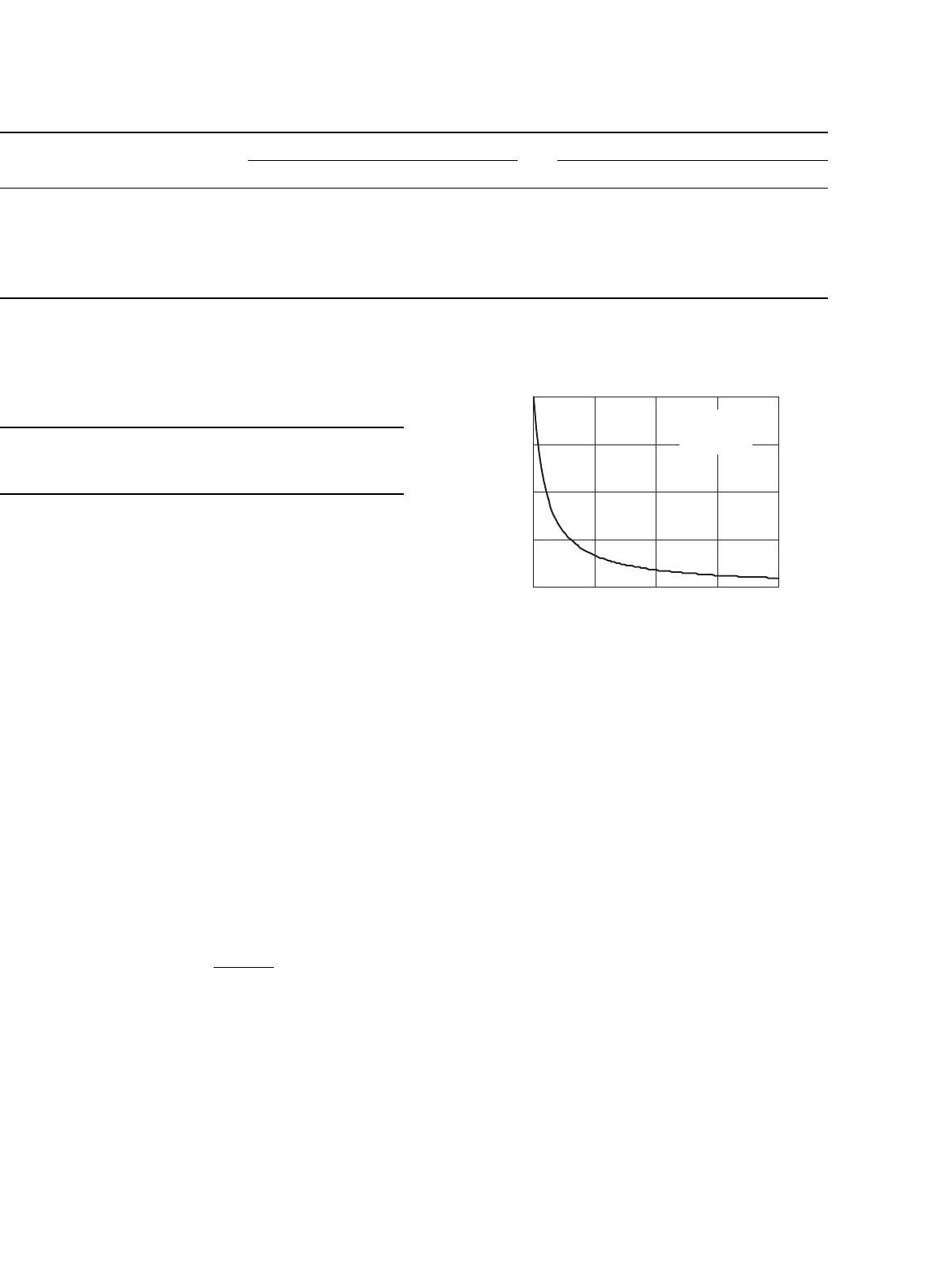
to fit the lamp resistance vs power characteristic is the hyper-
bolic approximation. For example, Mader and Horn propose
in [14] the following simple approximation:
R
LA
(P
LA
) =
V
2
0
P
LA
+P
0
(22.4)
where R
LA
is the equivalent lamp resistance, P
LA
is the average
lamp power, and V
0
and P
0
are two parameters which depend
on each lamp. This characteristic has been plotted in Fig. 22.15
for a particular lamp with V
0
= 100 V and P
0
= 1W.
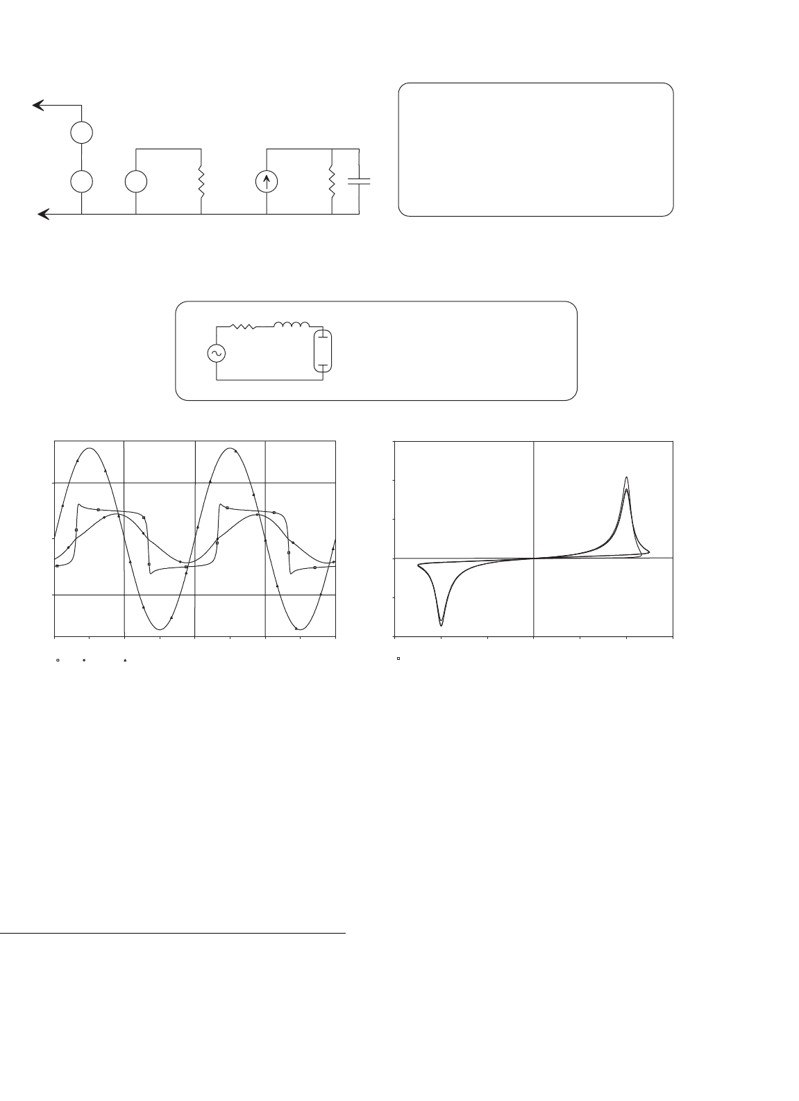
This model can be implemented very easily in circuit simu-
lation programs, such as SPICE-based programs. Figure 22.16
shows the electric circuit and the description used to model
0 5 10 15 20
0
2500
5000
7500
10000
R
LA
(Ω)
P
LA
(W)
V
0
=100 V
P
0
=1 W
FIGURE 22.15 Lamp resistance vs lamp power characteristic.
the lamp behavior in a SPICE-based simulation program. The
voltage-controlled voltage source EL is used to model the resis-
tive behavior of the lamp. The voltage source VS is used to
measure the lamp current so that the instantaneous and aver-
age lamp current can be calculated; for this reason its voltage
value is equal to zero. GP is a voltage-controlled current source
used to calculate the instantaneous lamp power, which is then
filtered by RP and CP in order to obtain the averaged lamp
power. Finally, the hyperbolic relationship between the lamp
resistance and power is implemented by means of the voltage-
controlled voltage source EK. The time constant τ = RP·CP is
related to the ionization constant of the discharge.
Figure 22.17 illustrates some simulation results at low fre-
quency when the lamp is supplied from a sinusoidal voltage
source and stabilized with an inductive ballast.
The Mader–Horn model can also be used at high frequen-
cies obtaining a resistive behavior for the lamp. The equivalent
lamp resistance at high frequency will also exhibit a hyper-
bolic variation with the averaged lamp power and with a time
constant given by τ. This model is then useful to simulate
electronic ballast with dimming feature.
578 J. M. Alonso
10
20
15
EL
EK RK
30 40
GP RP CP
(a)
(b)
EK 30 20 Value={Vo*Vo/(V(40,20)+Po)}
.subckt lamp 10 20
+ params: Vo=100 Po=1 Tau=0.3m
EL 10 15 Value={V(30,20)*I(VS)}
VS 15 20 0
RK 30 20 1
GP 20 40 Value={V(10,20)*I(VS)}
RP 40 20 1
CP 40 20 {Tau}
.ends
VS
+
++ +
FIGURE 22.16 (a) Mader–Horn linear model for discharge lamps and (b) SPICE description of the model.
20ms 25ms 30ms 35ms 40ms 45ms 50ms 55ms 60ms
Time
v(2) i(lb)*50 v(1)
200
0
−200
−150V −100V −50V −0V 50V 100V 150V
v(2)
i(lb)
3.0A
2.0A
1.0A
0A
−1.0A
−2.0A
(b)
(c)
1
+
2
2a
LAMP
V
0
=100 V
P
0
=1 W
τ = 0.3 ms
Vg
0
Vg 1 0 SIN(0 325 50)
Rb 1 2a 100
Lb 2a 2 500mH
XLA 2 0 LAMP
.tran 0.1m 60m 0 0.1m
(a)
Rb
Lb
FIGURE 22.17 (a) Example of simulation with an inductive ballast at low frequency; (b) operating waveforms; and (c) lamp I–V characteristics.
Discharge lamp modeling has become an important subject,
since its results are very useful to optimize the electronic ballast
performance. Some improvements on the Mader–Horn model
and other interesting models can be found in the literature
[14–16].
22.4 Resonant Inverters for Electronic
Ballasts
Most modern domestic and industrial electronic ballasts use
resonant inverters to supply discharge lamps. They can be
implemented in two basic ways: current-fed resonant inverters
and voltage-fed resonant inverters.
22.4.1 Current-fed Resonant Inverters
One of the most popular topologies belonging to this cate-
gory is the current-fed push–pull resonant inverter, previously
shown in Fig. 22.11. For this reason, this inverter will be stud-
ied here to illustrate the operation of the current-fed resonant
ballasts.
The current-fed push–pull inverter uses an input choke to
obtain a DC input current with low current ripple. This current
is alternatively conducted by the switches so that a parallel
22 Electronic Ballasts 579
i
s
L
C
−
+
+
v
o
I
s
−I
s
i
s
v
o
Fundamental (I
s,1
)
(a) (b)
ϕ
π
2π
ωt
R
FIGURE 22.18 (a) Equivalent circuit of a current-fed parallel resonant inverter and (b) operating waveforms.
resonant tank can be supplied with a current square wave.
Figure 22.18 shows the equivalent circuit and the operating
waveforms of a current-fed parallel resonant inverter.
The input current can be expressed as a Fourier series in the
following way:
i
s
(t) =
n=1,3,5...
I
S,n
sin nωt =
n=1,3,5...
4I
S
nπ
sin nωt (22.5)
I
S,n
being the peak value of each current harmonic and I
S
the
DC input current of the inverter. The output voltage for each
current harmonic is obtained by multiplying the input current
I
S,n
by the equivalent parallel impedance Z
E,n
, this is:
V
0,n
= I
S,n
Z
E,n
= I
S,n
1
1/R +jnωC − j(1/nωL)
(22.6)
Usually, normalized values are employed in order to provide
more general results. Then, the output voltage can be expressed
as follows:
V
0,n
= I
S,n
Z
B
1
1/Q +jn −j(1/n)
(22.7)
where Z
B
is the base impedance of the resonant tank, Q is the
normalized load, is the normalized frequency, and ω
0
is the
natural frequency of the resonant circuit, given by:
Z
B
=
√
L/CQ= R/Z
B
= ω/ω
0
= ω
√
LC ω
0
= 1/
√
LC
(22.8)
From Eq. (22.7) the peak output voltage V
0,n
and phase angle
ϕ
n
can be obtained for each harmonic:
V
0,n
= I
S,n
Z
B
1
1/Q
2
+(n −1/n)
2
(22.9)
ϕ
n
=−tan
−1
Q(n −1/n) (22.10)
The total harmonic distortion (THD) of the output voltage
can be calculated as follows:
THD(%) =
n=3,5,7...
V
2
0,n
V
0,1
·100 (22.11)
Based on these equations, the analysis and design of the
current-fed resonant inverter can be performed. Normally, the
circuit operates close to the natural frequency ω
0
and the effect
of the high frequency harmonics can be neglected. To probe
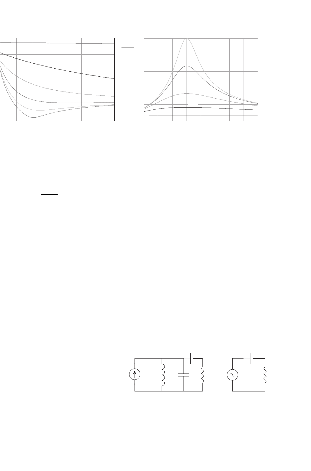
this, Fig. 22.19a illustrates the THD of the output voltage as
a function of the normalized load and frequency, obtained by
plotting Eq. (22.11). As can be seen, for values of Q higher than
1 and for operation close to the natural frequency ( = 1), the
THD is low, which means that the output voltage is nearly a
sinusoidal waveform. However, for low values of Q, the out-
put voltage tends to be a square waveform and the THD tends
to the value of about 48%, corresponding to the THD of
a square waveform. Figure 22.19b illustrates the normalized
output voltage for the fundamental component.
As stated previously, when used as lamp ballast, the current-
fed parallel resonant inverter operates at the natural frequency
of the resonant tank to both ignite the lamp and limit the
current at normal running. Neglecting the effect of high-order
harmonics, the rms output voltage is given by the fundamental
component, and can be obtained using = 1 in Eq. (22.9) as
follows:
V
0(rms)
≈ V
0,1(rms)
= I
S,1(rms)
Z
B
Q =
4I
S
R
π
√
2
(22.12)
In a current-fed resonant inverter, the DC input current I
S
is supplied from a DC voltage source V
in
with a series choke, as
stated previously. Then, the DC input current can be obtained,
assuming 100% efficiency, by equaling input and output power
as follows:
P
in
= V
in
I
S
=
V
2
0(rms)
R
(22.13)
580 J. M. Alonso
0.6 0.8 1 1.2 1.4 1.6 1.8 2
0
10
20
30
40
50
0.2
0.5
1
2
7
Ω
Q=0.01
THD(%)
0.4 0.6 0.8 1 1.2 1.4 1.6 1.8 2
0
0.6
1.2
1.8
2.4
3
0.2
0.5
1
2
Q=3
Ω
V
0,1
I
S,1
Z
B
(b)(a)
FIGURE 22.19 Characteristics of the current-fed parallel resonant inverter: (a) THD and (b) fundamental output voltage.
and then:
I
S
=
V
2
0(rms)
V
in
R
(22.14)
using Eq. (22.14) in Eq. (22.12) and solving for the output
voltage:
V
0(rms)
=
π
√
2
4
V
in
= 1.1V
in
(22.15)
As can be seen, when operating at the natural frequency,
the rms output voltage is independent of the resonant tank
load. The peak output voltage is equal to πV
in
/2. This value is
directly related to the peak voltage stress in the switches. For
a full-bridge topology, as shown in Fig. 22.11c, this value is
equal to the switch voltage stress. However, for the current-
fed push–pull inverter, the voltage stress is twice this value,
this is πV
in
, due to the presence of the transformer. This gives
a very high voltage stress for the switches in this topology, this
is the reason why the current-fed push–pull is mainly used to
implement low input voltage ballasts.
On the other hand, lamp starting voltage can vary from 5
to 10 times the lamp voltage in normal discharge mode. This
makes difficult the use of the current-fed parallel resonant
inverter at constant frequency to both ignite the lamp and
supply it at steady state, since the output voltage is independent
of the resonant tank load.
One solution to this problem is to ignite the lamp at the res-
onant tank natural frequency and then change the frequency
to decrease the output voltage and output current to the nor-
mal running values of the lamp. This solution makes necessary
the use of extra circuitry to control the frequency, normally in
closed loop to avoid lamp instabilities, which increases the
ballast cost.
Another solution, very often used in low cost ballasts, is to
design the parallel resonant tank to ignite the lamp, and limit
the lamp current in discharge mode by using an additional
reactive element in series with the lamp. Normally a capacitor
is used to limit the lamp current in order to minimize the
cost of the ballast. This solution is used in combination with
the self-oscillating technique, which assures the operation at
a constant frequency equal to the natural frequency of the
resonant tank. Figure 22.20a illustrates this circuit. Normally
the effect of the series capacitor is neglected and the resonant
tank is assumed to behave as a sinusoidal voltage source during
both ignition and normal operation, as shown in Fig. 22.20b.
The high lamp starting voltage is obtained by means of a step-
up transformer, this is why typically a push–pull topology is
used. If V
in
is the DC input voltage and V
ig
is the lamp ignition
voltage, then the necessary transformer turn ratio is given by
the following expression:
N
2
N
1
=
V
ig
πV
in
/2
(22.16)
i
S
L
+
(a)
C
S
RRC
(b)
1.1 V
in
C
S
+
FIGURE 22.20 (a) Typical parallel resonant circuit used to supply
discharge lamps and (b) equivalent circuit.