Power electronic handbook
Подождите немного. Документ загружается.

520 I. Batarseh and H. Wei
As we can see from Eqs. (19.8) and (19.9), PF and THD
are related to distortion and displacement factors. Therefore,
improvement in PF, i.e. power factor correction (PFC), also
implies harmonic reduction.
19.3 Power Factor Correction
19.3.1 Energy Balance in PFC Circuits
Figure 19.3 shows a diagram of an ac–dc PFC unit. Let v
l
(t)
and i
l
(t) be the line voltage and line current, respectively.
For an ideal PFC unit (PF = 1), we assume
v
l
(t) = V
lm
sin ω
l
t (19.10a)
i
l
(t) = I
lm
sin ω
l
t (19.10b)
Power
Factor
Corrector
To power
converter
−v
l
(t) +
i
l
(t)
FIGURE 19.3 Block diagram of ac–dc PFC unit.
| v
l
(t) |
| i
l
(t) |
t
p
in
(t)
P
o
=P
in
1
/
2
Li
L
2(t)
W
ex
(t)
t
t
T
l
/2 T
l
3T
l
/4
I
II
W
ex,max
T
l
/4 3T
l
/8T
l
/8
FIGURE 19.4 Energy balance in PF corrector.
where, V
lm
and I
lm
are amplitudes of line voltage and line
current, respectively, and ω
l
is the angular line frequency.
The instantaneous input power is given by
p
in
(t) = V
lm
I
lm
sin
2
ω
l
t = P
in
(
1 −cos 2ω
l
t
)
(19.11)
where, P
in
= 1/2V
lm
I
lm
is the average input power.
As we can see from Eq. (19.11), the instantaneous input
power contains not only the real power (average power) P
in
component but also an alternative component with frequency
2ω
l
(i.e. 100 or 120 Hz), shown in Fig. 19.4. Therefore, the
operation principle of a PFC circuit is to process the input
power in a certain way that it stores the excessive input energy
(area I in Fig. 19.4) when p
in
(t) is larger than P
in
(=P
o
), and
releases the stored energy when p
in
(t) is less than P
in
(=P
o
)to
compensate for area II.
The instantaneous excessive input energy, w(t), is given by
w
ex
(
t
)
=
P
o
2ω
l
(
1 −sin 2ω
l
t
)
(19.12)
At t = 3T
l
/8, the excessive input energy reaches the peak
value
w
ex,max
=
P
o
ω
l
(19.13)
The excessive input energy has to be stored in the dynamic
components (inductor and capacitor) in the PFC circuit.
19 Power Factor Correction Circuits 521
In most of the PFC circuits, an input inductor is used to carry
the line current. For unity PF, the inductor current (or aver-
aged inductor current in switch mode PFC circuit) must be a
pure sinusoidal and in phase with the line voltage. The energy
stored in the inductor (1/2Li
2
L
(t)) cannot completely match the
change of the excessive energy as shown in Fig. 19.4. There-
fore, to maintain the output power constant, another energy
storage component (usually the output capacitor) is needed.
19.3.2 Passive Power Factor Corrector
Because of their high reliability and high power handling capa-
bility, passive power factor correctors are normally used in
high power line applications. Series tuned LC harmonic filter
is commonly used for heavy plant loads such as arc furnaces,
metal rolling mills, electrical locomotives, etc. Figure 19.5
shows a connection diagram of harmonic filter together with
line frequency switched reactor static VAR compensator. By
tuning the filter branches to odd harmonic frequencies, the
filter shunts the harmonic currents. Since each branch presents
capacitive at line frequency, the filter also provides capacitive
VAR for the system. The thyristor-controlled reactor keeps an
optimized VAR compensation for the system so that higher
PF can be maintained.
The design of the tuned filter PF corrector is particularly
difficult because of the uncertainty of the system impedance
and harmonic sources. Besides, this method involves too many
expensive components and takes huge space.
For the applications where power level is less than 10 kW,
the tuned filter PF corrector may not be a better choice. The
most common off-line passive PF corrector is the inductive-
input filter, shown in Fig. 19.6. Depending on the filter
inductance, this circuit can give a maximum of 90% PF. For
operation in continuous conduction mode (CCM), the PF is
defined as [11]
PF =
0.9
1 +
(
0.075/K
1
)
2
(19.14)
5th 7th 11th 13th
Harmonic Filters
Reactor
SCR
Load
Static VAR
Compensator
ac line
FIGURE 19.5 Series tuned LC harmonic filter PF corrector.
v
l
(t)
L
C
R
FIGURE 19.6 Inductive-input PF corrector.
where
K
1
=
ω
l
L
πR
(19.15)
The PF corrector is simply a low pass inductive filter
as shown in Fig. 19.7, whose transfer function and input
impedance are given by
H
(
s
)
=
1
s
2
LC +sL/R +1
(19.16)
Z
in
(
s
)
= R
s
2
LC +sL/R +1
sRC +1
(19.17)
The above equations show that the unavoidable phase dis-
placement is incurred in the inductive-filter corrector. Because
the filter frequency of operation is low (line frequency), large
value inductor and capacitor have to be used. As a result,
the following disadvantages are presented in most passive PF
correctors:
(a) Only less than 0.9 PF can be achieved;
(b) THD is high;
(c) They are heavy and bulky;
(d) The output is unregulated;
(e) The dynamic response is poor;
(f) They are sensitive to circuit parameters;
(g) Optimization of the design is difficult.
L
C
R
+
v
in
(t)
_
Z
in
+
v
o
(t)
_
FIGURE 19.7 Low pass inductive filter.
522 I. Batarseh and H. Wei
19.3.3 Basic Circuit Topologies of Active Power
Factor Correctors
In recent years, using the switched-mode topologies, many
circuits and control methods are developed to comply with
certain standard (such as IEEE Std 519 and IEC1000-3-2).
To achieve this, high-frequency switching techniques have
been used to shape the input current waveform success-
fully. Basically, the active PF correctors employ the six basic
converter topologies or their variation versions to accom-
plish PFC.
A. The Buck Corrector
Figure 19.8a shows the buck PF corrector. By using PWM
switch modeling technique [12], the circuit topology can be
modeled by the equivalent circuit shown in Fig. 19.8b. It
should be pointed out that the circuit model is a large signal
model, therefore analysis of PF performance based on this
model is valid. It can be shown that the transfer function and
input impedance are given by
H
(
s
)
=
d
s
2
LC +sL/R +1
(19.18)
Z
in
(
s
)
=
R
d
2
s
2
LC +sL/R +1
sRC +1
(19.19)
where d is the duty ratio of the switching signal.
v
l
(t)
L
C
R
S
D
(a)
L
CR
+
_
i
L
(t)
+
v
in
(t)
_
di
L
(t)
dv
in
(t)
Z
in
+
v
o
(t)
_
(
b
)
FIGURE 19.8 (a) Buck corrector and (b) PWM switch model for buck
corrector.
Notice that Eqs. (19.18) and (19.19) are different from
Eqs. (19.16) and (19.17), in that they have introduced the
control variable d. By properly controlling the switching duty
ratio to modulate the input impedance and the transfer func-
tion, a pure resistive input impedance and constant output
voltage can be approached. Thereby, unity PF and output reg-
ulation can both be achieved. These control techniques will be
discussed in the next section.
Comparing with the other type of high frequency PFC
circuits, the buck corrector offers inrush-current limiting,
overload or short-circuit protection, and over-voltage pro-
tection for the converter due to the existence of the power
switch in front of the line. Another advantage is that the out-
put voltage is lower than the peak of the line voltage, which
is usually the case normally desired. The drawbacks of using
buck corrector may be summarized as follows:
(a) When the output voltage is higher than the line volt-
age, the converter draws no current from the line,
resulting in significant line current distortion near the
zero-across of the line voltage;
(b) The input current is discontinuous, leading to high
differential mode EMI;
(c) The current stress on the power switch is high;
(d) The power switch needs a floating drive.
B. The Boost Corrector
The boost corrector and its equivalent PWM switch modeling
circuit are shown in Figs. 19.9a and b. Its transfer function and
v
l
(t)
L
C
R
S
D
(a)
CR
+
v
in
(t)
_
di
L
(t)
dv
o
(t)
Z
in
+
v
o
(t)
_
L
i
L
(t)
(
b
)
FIGURE 19.9 (a) Boost corrector and (b) PWM switch model of boost
corrector.
19 Power Factor Correction Circuits 523
input impedance are given by
H
(
s
)
=
1/d
s
2
L/d
2
C +s
L/d
2
/R +1
(19.20)
Z
in
(
s
)
= d
2
R
s
2
L/d
2
C +s
L/d
2
/R +1
sRC +1
(19.21)
where d
= 1 −d.
Unlike in the buck case, it is interesting to note that in
the boost case, the equivalent inductance is controlled by the
switching duty ratio. Consequently, both the magnitude and
the phase of the impedance, and both the dc gain and the
pools of the transfer function are modulated by the duty ratio,
which implies a tight control of the input current and the
output voltage. Other advantages of boost corrector include
less EMI and lower switch current and grounded drive. The
shortcomings with the boost corrector are summarized as:
(a) The output voltage must be higher than the peak of line
voltage;
(b) Inrush-current limiting, overload, and over-voltage
protections are not available.
C. The Buck–Boost Corrector
The buck–boost corrector and its equivalent circuit are shown
in Figs. 19.10a and b. The expressions for transfer function
v
l
(t)
L
C
R
SD
(a)
CR
+
v
in
(t)
_
d i
L
(t)
d v
o
(t)
Z
in
_
v
o
(t)
+
L
i
L
(t)
+
_
(
b
)
FIGURE 19.10 (a) Buck–boost corrector and (b) PWM switch model
of buck–boost corrector.
and input impedance are
H
(
s
)
=
d/d
s
2
L/d
2
C +s
L/d
2
/R +1
(19.22)
Z
in
(
s
)
=
d
d
2
R
s
2
L/d
2
C +s
L/d
2
/R +1
sRC +1
(19.23)
The buck–boost corrector combines some advantages of the
buck corrector and the boost corrector. Like a buck corrector,
it can provide circuit protections and step-down output volt-
age, and like a boost corrector its input current waveform
and output voltage can be tightly controlled. However, the
buck–boost corrector has the following disadvantages:
(a) The input current is discontinued by the power switch,
resulting in high differential mode EMI;
(b) The current stress on the power switch is high;
(c) The power switch needs a floating drive;
(d) The polarity of output voltage is reversed.
D. The Cuk, Sepic, and Zeta Correctors
Unlike the previous converters, the Cuk, Sepic, and Zeta
converters are fourth-order switching-mode circuits. Their cir-
cuit topologies for PFC are shown in Figs. 19.11a, b, and c,
respectively. Because there are four energy storage components
available to handle the energy balancing involved in PFC, sec-
ond harmonic output voltage ripples of these correctors are
smaller when compared with the second-order buck, boost,
and buck–boost topologies. These PF correctors are also able
to provide overload protection. However, the increased count
of components and current stress are undesired.
19.3.4 System Configurations of PFC
Power Supply
The most common configurations of ac–dc power supply with
PFC are two-stage scheme and one-stage (or single-stage)
scheme. In two-stage scheme as shown in Fig. 19.12a, a non-
isolated PFC ac–dc converter is connected to the line to create
an intermediate dc bus. This dc bus voltage is usually full
of second harmonic ripple. Therefore, followed by the ac–dc
converter, a dc–dc converter is cascaded to provide electrical
isolation and tight voltage regulation. The advantage of two-
stage structure PFC circuits is that the two power stages can be
controlled separately, and thus it makes it possible to have both
converters optimized. The drawbacks of this scheme are lower
efficiency due to twice processing of the input power, complex
control circuits, higher cost, and low reliability. Although the
two-stage scheme approach is commonly adopted in industry,
it received limited attention by the common research, since
the input stage and output stage can be studied independently.
One-stage scheme combines the PFC circuit and power con-
version circuit in one stage as shown in Fig. 19.12b. Due to its
524 I. Batarseh and H. Wei
v
l
(t)
L
1
C
R
S
D
L
2
C
o
(a)
v
l
(t)
L
1
C
R
S
D
L
2
C
o
(b)
v
l
(t)
L
1
C
R
S
D
L
2
C
o
(c)
FIGURE 19.11 Fourth-order corrector: (a) Cuk corrector; (b) Sepic
corrector; and (c) Zeta corrector.
simplified structure, this scheme is potentially more efficient
and is very attractive in low to medium power level appli-
cations, particularly in those cost-sensitive applications. The
one-stage scheme, therefore becomes the main stream of con-
temporary research due to the ever-increasing demands for
inexpensive power supply in residential and office appliance.
For many single-stage PFC converters, one of the most
important issues is the slow dynamic response under line and
load changes. To remove the low frequency ripple caused by
the line (120 Hz) from the output and keep a nearly constant
operation duty ratio, a large volume output capacitor is nor-
mally used. Consequently, a low frequency pole (typically less
than 20 Hz) must be introduced into the feedback loop. This
results in very slow dynamic response of the system [13, 14].
To avoid twice power process in two-stage scheme, two con-
verters can be connected in parallel to form so-called parallel
PFC scheme [15]. In parallel PFC circuit, power from the ac
main to the load flows through two parallel paths, shown in
Fig. 19.12c. The main path is a rectifier, in which power is not
ac-dc
converter with
PFC
i
l
(t)
dc-dc
regulator
Controller Controller
R
L
+
V
o
_
C
B
ac-dc converter with
both PFC and
regulation
− v
l
(t) +
i
l
(t)
Controller
R
L
+
V
o
_
Stage 1
Stage 2
Bulk
Capacitor
P
in
P
2
P
1
P
o
+
+
(a)
(b)
(c)
− v
l
(t) +
FIGURE 19.12 System configurations of PFC power supply: (a) two-
stage scheme; (b) one-stage scheme; and (c) parallel scheme.
processed twice for PFC, whereas the other path processes the
input power twice for PFC purpose. It is shown that to achieve
both unity PF and tight output voltage regulation, only the dif-
ference between the input and output power within a half cycle
(about 32% of the average input power) needs to be processed
twice [15]. Therefore, high efficiency can be obtained by this
method.
The continuous research in improving system PF has
resulted in countless circuit topologies and control strate-
gies. Classified by their principles to realize PFC, they can
be mainly categorized into discontinuous conduction mode
(DCM) input technique and continuous conduction mode
(CCM) shaping technique. The recent research interest in
DCM input technique is focused on developing PFC circuit
topologies with a single power switch, result in single-stage
single-switch converter (so-called S
4
-converter). The CCM
shaping technique emphasizes on the control strategy to
19 Power Factor Correction Circuits 525
active PFC technique
DCM input CCM shaping
current mode
voltage mode
peak
current
control
average
current
control
capacitor
voltage
control
inductor
voltage
control
system
configuration
conduction
mode
other
techniques
hysteresis
control
charge
control
nonlinear
carrier
control
one-
stage
two-
stage
S
4
-PFC
Parallel
FIGURE 19.13 Overview of PFC techniques.
achieve unity input PF. The hot topics in this line of research
are concentrated on degrading complexity of the control cir-
cuit and enhancing dynamic response of the system, resulting
in some new control methods. Figure 19.13 shows an overview
of these techniques based on conduction mode and system
configuration types.
19.4 CCM Shaping Technique
Like other power electronic apparatus, the core of a PFC unit
is its converter, which can operate either in DCM or in CCM.
As shall be discussed in the next section, the benefit from
DCM technique is that low-cost power supply can be achieved
because of its simplified control circuit. However, the peak
input current of a DCM converter is at least twice as high as
its corresponding average input current, which causes higher
current stresses on switches than that in a CCM converter,
resulting in intolerable conduction and switching losses as well
as transformer copper losses in high power applications. In
practice, DCM technique is only suitable for low to medium
level power application, whereas, CCM is used in high power
cases. However, a converter operating in CCM does not have
PFC ability inherently, i.e. unless a certain control strategy is
applied, the input current will not follow the waveform of line
voltage. This is why most of the research activities in improv-
ing PF under CCM condition have been focused on developing
new current shaping control strategies. Depending on the sys-
tem variable being controlled (either current or voltage), PFC
control techniques may be classified as current control and
voltage control. Current control is the most common control
strategy since the primary objective of PFC is to force the input
current to trace the shape of line voltage.
To achieve both PFC and output voltage regulation by using
a converter operating in CCM, multiloop controls are generally
used. Figure 19.14 shows the block diagram of ac–dc PFC
ac-dc
converter
(CCM)
Comp.
+
v
l
(t)
_
x(t)
H
x
H
l
Comp.
V
ref
+
V
o
_
x
a
Logic &
Drive
x
cmd
FIGURE 19.14 Block diagram of PFC converter with CCM shaping
technique.
converter with CCM shaping technique, where, H
l
is a line
voltage compensator, H
x
is a controlled variable compensator,
and x(t) is the control variable that can be either current or
voltage.
Normally, in order to obtain a sinusoidal line current and
a constant dc output voltage, line voltage v
l
(t), output voltage
V
o
, and a controlled variable x(t) need to be sensed. Depending
on whether the controlled variable x(t) is a current (usually the
line current or the switch current) or a voltage (related to the
line current), the control technique is called “current mode
control” or “voltage mode control,” respectively. In Fig. 19.14,
two control loops have been applied: the feedforward loop and
the feedback loops. The feedforward loop is also called “inner
loop” which keeps the line current to follow the line voltage in
shape and phase, while the feedback loop (also called “outer
loop”) keeps the output voltage to be tightly controlled. These
two loops share the same control command generated by the
product of output voltage error signal and the line voltage (or
rectified line voltage) signal.
526 I. Batarseh and H. Wei
19.4.1 Current Mode Control
Over many years, different current mode control techniques
were developed. In this section, we will review several known
methods.
A. Average Current Control
In average current control strategy, the average line current
of the converter is controlled. It is more desired than the
other control strategies because the line current in a SMPS can
be approximated by the average current (per switching cycle)
through an input EMI filter. The average current control is
widely used in industries since it offers improved noise immu-
nity, lower input ripple, and stable operation [13, 16–19].
Figure 19.15 shows a boost PFC circuit using average current
control strategy. In the feedforward loop, a low value resistor
R
s
is used to sense the line current. Through the op-amp net-
work formed by R
i
, R
imo
, R
f
, C
p
, C
z
, and A
2
, average line
current is detected and compared with the command current
signal, i
cmd
, which is generated by the product of line voltage
signal and the output voltage error signal.
There is a common issue in CCM shaping technique, i.e.
when the line voltage increases, the line voltage sensor pro-
vides an increased sinusoidal reference for the feedforward
loop. Since the response of feedback loop is much slow than
the feedforward loop, both the line voltage and the line cur-
rent increase, i.e. the line current is heading to wrong changing
direction (with the line voltage increasing, the line current
should decrease). This results in excessive input power, caus-
ing overshoot in the output voltage. The square block, x
2
,in
the line voltage-sensing loop shown in Fig. 19.15 provides a
typical solution for this problem. It squares the output of the
low-pass filter (LPF), which is in proportion to the amplitude
of the line voltage, and provides the divider (A ∗ B)/C with a
squared line voltage signal for its denominator. As a result, the
Load
Gate
Drive
k
1
A*B
C
A
2
_
+
A
1
_
+
x
2
LPF
V
ref
PWM
Line
R
s
+ −
R
imo
R
i
R
f
C
z
C
p
i
1
(t)
AB
C
+ −
i
1
(t)
i
l
(t)
i
cmd
Σ
FIGURE 19.15 Boost corrector using average current control.
amplitude of the sinusoidal reference i
cmd
is negatively propor-
tional to the line voltage, i.e. when the line voltage changes, the
control circuit leads the line current to change in the opposite
direction, which is the desired situation. The detailed analysis
and design issues can be found in [16–18].
As it can be seen, the average current control is a very
complicated control strategy. It requires sensing the inductor
current, the input voltage, and the output voltage. An amplifier
for calculating the average current and a multiplier are needed.
However, because of today’s advances made in IC technology,
these circuits can be integrated in a single chip.
B. Variable Frequency Peak Current Control
Although the average current control is a more desired strat-
egy, the peak current control has been widely accepted because
it improves the converter efficiency and has a simpler control
circuit [14, 20–24]. In variable frequency peak control strat-
egy, shown in Fig. 19.16, the output error signal k(t)isfed
Line
V
ref
Logic
& drive
ac-dc
converter
S
H
(s)
A
1
−
+
A
2
+
β
α
−
v
1
(t)
i
1
(t)
+
V
o
−
i
1
(t)
v
1
(t)
i
cmd
(t)
k(t)
i
l
(t)
+
−
FIGURE 19.16 Block diagram for variable frequency peak current
control.
19 Power Factor Correction Circuits 527
back through its outer loop. This signal is multiplied by the
line voltage signal αv
1
(t) to form a line current command
signal i
cmd
(t)(i
cmd
(t)=αk(t) · v
1
(t)). The command signal
i
cmd
(t) is the desired line current shape since it follows the
shape of the line voltage. The actual line current is sensed by a
transducer, resulting in signal βi
1
(t) that must be reshaped to
follow i
cmd
(t) by feeding it back through the inner loop. After
comparing the line current signal βi
1
(t) with the command
signal i
cmd
(t), the following control strategies can be realized,
depending on its logic circuit:
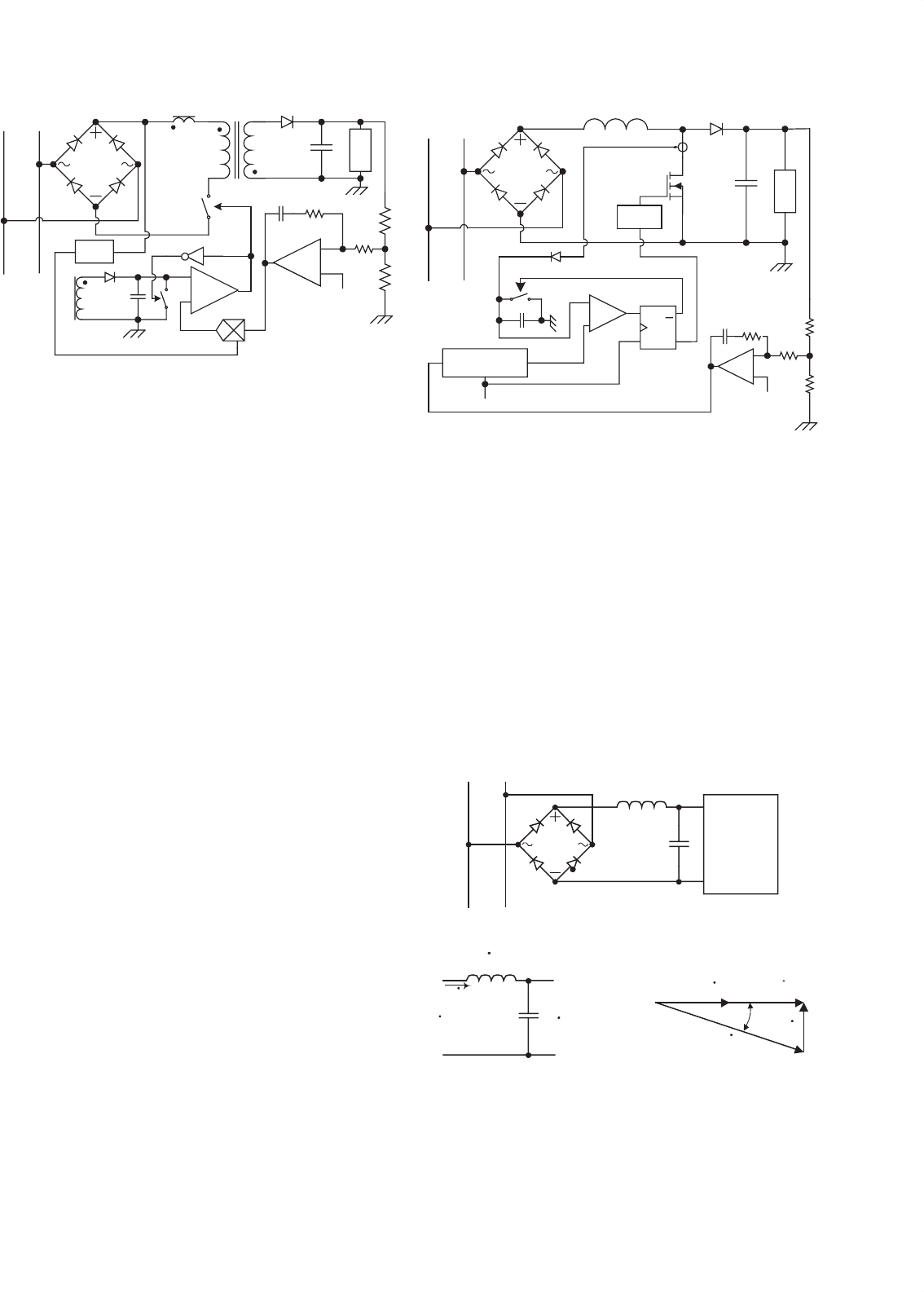
Constant on-time control: Its input current waveform is given
in Fig. 19.17a. Letting the fixed on-time to be T
s
, the control
rules are:
• At t = t
k
when βi
1
(t
k
) = i
cmd
(t
k
), S is turned on;
•
At t = t
k
+T
on
, S is turned off.
Constant off-time control: The input current waveform is
shown in Fig. 19.17b. Assuming the off-time is T
off
, the control
rules are:
• At t = t
k
when βi
1
(t
k
) = i
cmd
(t
k
), S is turned off;
• At t=t
k
+T
off
, S is turned on.
C. Constant Frequency Peak Current Control
Generally speaking, to make it easier to design the EMI filter
and to reduce harmonics, constant switching frequency ac–dc
t
k
t
k+2
T
on
T
on
i
cmd
(t)
β
i
1
(t)
t
t
k
+T
on
t
k+1
(a)
t
k
t
k+1
t
k+2
T
off
T
off
i
cmd
(t)
βi
1
(t)
t
(b)
FIGURE 19.17 Input current waveforms for variable frequency peak
current control: (a) constant on-time control and (b) constant off-time
control.
Q
Q
SET
CLR
S
R
Logic
& drive
A
2
+
−
i
1
(t)
v
1
(t)
i
cmd
(t)
k(t)
CP
α
β
FIGURE 19.18 Logic circuit for constant frequency peak current
control.
PFC converter is preferred. Based on the block diagram shown
in Fig. 19.18, with T
s
is the switching period, the following
control rules can be considered to realize a constant frequency
peak current control (shown in Fig. 19.19b):
• At t = nT
s
, S is turned on;
•
At t = t
n
when βi
1
(t
n
) = i
cmd
(t
n
), S is turned off.
Line
V
ref
Logic
& drive
ac-dc
converter
S
H(s)
A
1
−
+
A
2
+
+
−
v
1
(t)
i
1
(t)
+
V
o
i
cmd
(t)
k(t)
Stabilizing
ramp
Q
Q
SET
CLR
S
R
i
l
(t)
−
−
i
1
(t)
β
α
v
1
(t)
nT
s
i
cmd
(t)
t
(n+1)T
s
(n+2)T
s
t
n
t
n+1
(a)
(b)
β
i
1
(t)
FIGURE 19.19 (a) Constant frequency peak current control with sta-
bilizing ramp compensation and (b) line current waveform for constant
frequency peak current control.
528 I. Batarseh and H. Wei
The logic circuit for the above control rules can be real-
ized by using an R–S flip-flop with a constant frequency
setting clock pulse (CP), as shown in Fig. 19.18. Unfortu-
nately, this logic circuit will result in instability when the duty
ratio exceeds 50%. This problem can be solved by subtracting
a stabilizing ramp signal from the original command signal.
Figure 19.19a shows a complete block diagram for typical con-
stant frequency peak current control strategy. The line current
waveform is shown in Fig. 19.19b.
It should be noticed that in both variable frequency and
constant frequency peak current control strategies, either the
input current or the switch current could be controlled. Thus
it makes possible to apply these control methods to buck type
converters. There are several advantages of using peak current
control:
• The peak current can be sensed by current transformer,
resulting in reduced transducer loss;
• The current-error compensator for average control
method has been eliminated;
• Low gain in the feedforward loop enhances the system
stability;
• The instantaneous pulse-by-pulse current limit leads to
increased reliability and response speed.
However the three signals, line voltage, peak current, and
output voltage signals, are still necessary to be sensed and
multiplier is still needed in each of the peak current con-
trol method. Comparing with the average current control
method, the input current ripple of these peak current con-
trol methods may be high when the line voltage is near
the peak value. As a result, considerable line current distor-
tion exists under high line voltage and light low operation
conditions.
D. Hysteresis Control
Unlike the constant on-time and the constant off-time con-
trol, in which only one current command is used to limit
either the minimum input current or the maximum input
current, the hysteresis control has two current commands,
i
hcmd
(t) and i
lcmd
(t)(i
lcmd
(t) = δi
hcmd
(t)), to limit both
the minimum and the maximum of input current [25–28].
To achieve smaller ripple in the input current, we desire a
narrow hyster-band. However, the narrower the hyster-band,
the higher the switching frequency. Therefore, the hyster-
band should be optimized based on circuit components such
as switching devices and magnetic components. Moreover,
the switching frequency varies with the change of line volt-
age, resulting in difficulty in the design of the EMI filter.
The circuit diagram and input current waveform are given
in Figs. 19.20a and b, respectively. When βi
1
(t) ≥ i
hcmd
(t),
a negative pulse is generated by comparator A
1
to reset the
R–S flip-flop. When βi
1
(t) ≤ i
lcmd
(t), a negative pulse is
(a)
t
k
t
k
+T
s
i
hcmd
(t)
β i
1
(t)
t
i
lcmd
(t)
t
k+1
(b)
Line
V
ref
Logic
& drive
ac-dc
converter
S
H(s)
A
o
+
−
A
1
+
v
1
(t)
i
1
(t)
+
V
o
−
i
1
(t)
a
v
1
i
lcmd
(t)
k(t)
Q
Q
SET
CLR
S
R
A
2
i
hcmd
(t)
+
−
+
−
δ
β
FIGURE 19.20 Hysteresis control: (a) block diagram for hysteresis
control and (b) line current waveform of hysteresis control.
generated by comparator A
2
to set the R–S flip-flop. The
control rules are:
• At t = t
k
when βi
1
(t
k
) = i
lcmd
(t), S is turned on;
•
At t = t
k+1
βi
1
(t
k+1
) = i
hcmd
(t), S is turned off;
• When βi
1
(t) = i
hcmd
(t) = i
lcmd
(t), S stays off or on.
Like the above mentioned peak current control meth-
ods, the hysteresis control method has simpler implementa-
tion, enhanced system stability, and increased reliability and
response speed. In addition, it has better control accuracy
than that the peak current control methods have. However,
this improvement is achieved on the penalty of wide range
of variation in the switching frequency. It is also possible
to improve the hysteresis control in a constant frequency
operation [29, 30], but usually this will increase the complexity
of the control circuit.
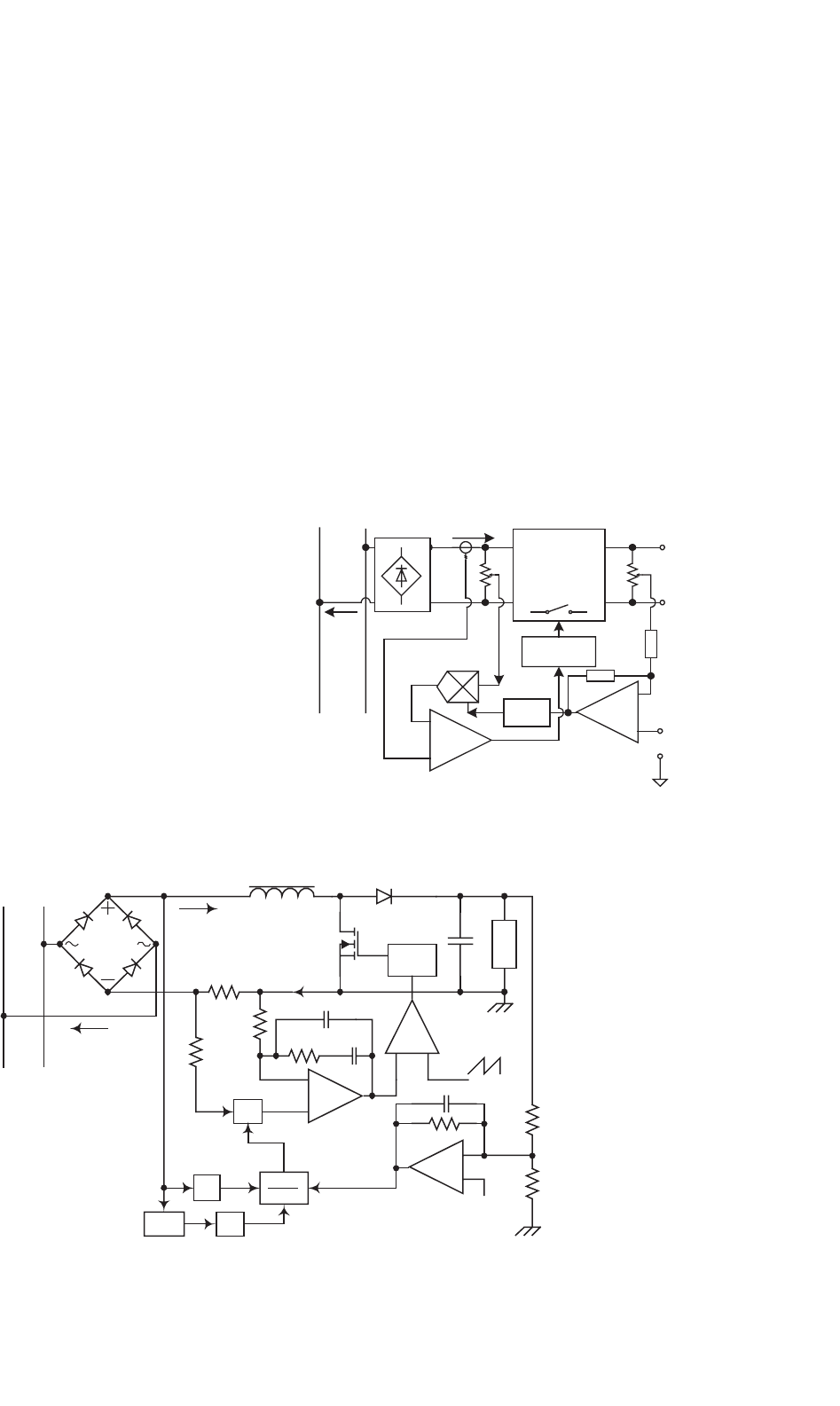
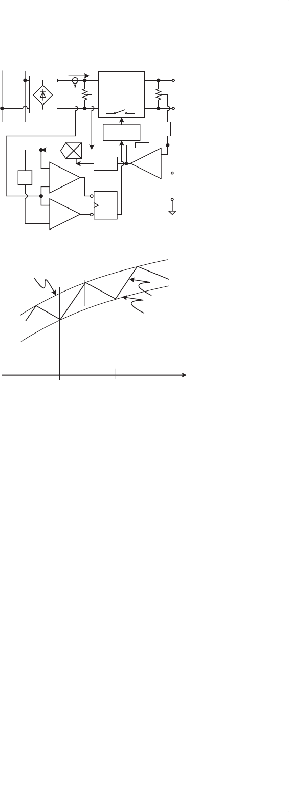
E. Charge Control
In order to make the average control method to be applicable
for buck-derived topologies where the switch current instead
19 Power Factor Correction Circuits 529
Line
V
ref
Load
1/k
1
T1
T1
S
T
Sd
V
o
C
T
A
2
+
−
A
1
v
c
+
−
FIGURE 19.21 Flyback PFC converter using charge control.
of the inductor current needs to be controlled, an alterna-
tive method to realize average current control, namely, charge
control was proposed in [31–33]. Since the total charge of the
switch current per switching cycle is proportional to the aver-
age value of the switch current, the average current can be
detected by a capacitor-switch network. Figure 19.21 shows
a block diagram for charge control. The switch current is
sensed by current transformer T1 and charges the capacitor
C
T
to form average line current signal. As the switch current
increases, the charge on capacitor C
T
also increases. When
the voltage reaches the control command v
c
, the power switch
turns off. At the same time, the switch S
d
turns on to reset
the capacitor. The next switching cycle begins with the power
switch turning on and the switch S
d
turning off by a clock
pulse.
The advantages of charge control are:
• Ability to control average switch current;
• Better switching noise immunity than peak current
control;
• Good dynamic performance;
• Elimination of turn off failure in some converters
(e.g. multiresonant converter) when the switch current
reaches its maximum value.
The disadvantages are:
• Synthesis of the reference v
c
still requires sensing both
input and output voltage and use of a multiplier;
•
Subharmonic oscillation may exist.
F. Non-linear-carrier (NLC) Control
To further simplify the control circuitry, non-linear-carrier
control methods were introduced [34, 35]. In CCM operation,
since the input voltage is related to the output voltage through
the conversion ratio, the input voltage information can be
recovered by the sensed output voltage signal. Thus the sensing
of input voltage can be avoided, and therefore, the multiplier is
Line
A
1
_
+
V
ref
Load
Carrier
Generator
L
S
Sd
V
o
C
T
Q
Q
SET
CLR
S
R
A
2
+
_
Drive
CP
D
C
FIGURE 19.22 Boost PFC converter using NLC control.
not needed, resulting in significant simplification in the control
circuitry. However, complicated NLC waveform generator and
its designs are involved. Figure 19.22 shows the block diagram
of the NLC charge control first introduced in [34].
19.4.2 Voltage Mode Control
Generally, current mode control is preferred in current source
driven converters, as the boost converter. To develop con-
trollers for voltage source driven converter, like the buck
converter and to improve dynamic response, voltage mode
control strategy was proposed [36, 37]. Figure 19.23 shows the
+ V
L
ac-dc
converter
C
i
L
i
line
(a)
(b) (c)
+
V
s
_
-
+
V
C
_
I
s
L
i
C
i
V
L
V
C
I
s
V
s
f
FIGURE 19.23 Input circuit and phasor diagram for voltage control:
(a) input circuit of voltage control ac–dc converter; (b) simplified input
circuit; and (c) phasor diagram.