Power electronic handbook
Подождите немного. Документ загружается.

2 The Power Diode 19
2.5 Snubber Circuits for Diode
Snubber circuits are essential for diodes used in switching
circuits. It can save a diode from overvoltage spikes, which
may arise during the reverse recovery process. A very com-
mon snubber circuit for a power diode consists of a capacitor
and a resistor connected in parallel with the diode as shown in
Fig. 2.7.
When the reverse recovery current decreases, the capac-
itor by virtue of its property will try to hold the voltage
across it, which, approximately, is the voltage across the diode.
The resistor on the other hand will help to dissipate some of
the energy stored in the inductor, which forms the I
RR
loop.
The dv/dt across a diode can be calculated as:
dv
dt
=
0.632 ×V
S
τ
=
0.632 ×V
S
R
S
×C
S
(2.2)
where V
S
is the voltage applied across the diode.
Usually the dv/dt rating of a diode is given in the manufac-
turers datasheet. Knowing dv/dt and the R
S
, one can choose
the value of the snubber capacitor C
S
. The R
S
can be calculated
from the diode reverse recovery current:
R
S
=
V
S
I
RR
(2.3)
The designed dv/dt value must always be equal or lower than
the dv/dt value found from the datasheet.
C
s
R
s
V
s
FIGURE 2.7 A typical snubber circuit.
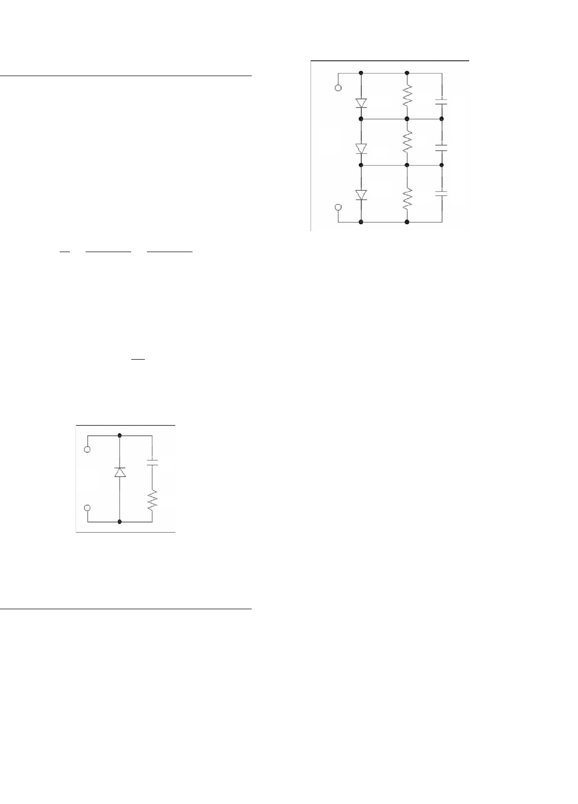
2.6 Series and Parallel Connection of
Power Diodes
For specific applications, when the voltage or current rating
of a chosen diode is not enough to meet the designed rating,
diodes can be connected in series or parallel. Connecting them
in series will give the structure a high voltage rating that may
be necessary for high-voltage applications. However, one must
ensure that the diodes are properly matched especially in terms
of their reverse recovery properties. Otherwise, during reverse
recovery there may be a large voltage imbalances between the
C2
C1
C3
R3
R2
R1
D1
D2
D3
V
s
FIGURE 2.8 Series connected diodes with necessary protection.
series connected diodes. Additionally, due to the differences
in the reverse recovery times, some diodes may recover from
the phenomenon earlier than the other causing them to bear
the full reverse voltage. All these problems can effectively be
overcome by connecting a bank of a capacitor and a resistor
in parallel with each diode as shown in Fig. 2.8.
If a selected diode cannot match the required current rating,
one may connect several diodes in parallel. In order to ensure
equal current sharing, the designer must choose diodes with
the same forward voltage drop properties. It is also important
to ensure that the diodes are mounted on similar heat sinks
and are cooled (if necessary) equally. This will affect the tem-
peratures of the individual diodes, which in turn may change
the forward characteristics of diode.
Tutorial 2.1 Reverse Recovery and
Overvoltages
Figure 2.9 shows a simple switch mode power supply. The
switch (1-2) is closed at t =0 s. When the switch is open, a
freewheeling current I
F
=20 A flows through the load (RL),
freewheeling diode (DF), and the large load circuit inductance
(LL). The diode reverse recovery current is 20 A and it then
decays to zero at the rate of 10 A/µs. The load is rated at 10
and the forward on-state voltage drop is neglected.
(a) Draw the current waveform during the reverse recov-
ery (I
RR
) and find its time (t
rr
).
(b) Calculate the maximum voltage across the diode
during this process (I
RR
).
S
OLUTION. (a) A typical current waveform during
reverse recovery process is shown in Fig. 2.10 for an
ideal diode.
When the switch is closed, the steady-state current is,
I
SS
= 200 V/10 = 20 A, since under steady-state con-
dition, the inductor is shorted. When the switch is open,
the reverse recovery current flows in the right-hand side
20 A. I. Maswood
DF
ldf
RL
I
LL
2
1
L=10uH
V
s
=200V
Is
+
−
FIGURE 2.9 A simple switch mode power supply with freewheeling
diode.
20A
0
s
20A
t1
t2
t3
time (s)
FIGURE 2.10 Current through the freewheeling diode during reverse
recovery.
loop consisting of the LL, RL, and DF. The load induc-
tance, LL is assumed to be shorted. Hence, when the
switch is closed, the loop equation is:
V = L
di
S
dt
from which
di
S
dt
=
V
L
=
200
10
= 20 A/µs
At the moment the switch is open, the same current
keeps flowing in the right-hand side loop. Hence,
di
d
dt
=−
di
S
dt
=−20 A/µs
from time zero to time t
1
the current will decay at a
rate of 20 A/s and will be zero at t
1
=20/20 =1 µs. The
reverse recovery current starts at this point and, accord-
ing to the given condition, becomes 20 A at t
2
. From
this point on, the rate of change remains unchanged at
20 A/µs. Period t
2
– t
1
is found as:
t
2
−t
1
=
20 A
20 A/µs
= 1 µs
From t
2
to t
3
, the current decays to zero at the rate of
20 A/µs. The required time:
t
3
−t
2
=
20 A
10 A/µs
= 2 µs
Hence the actual reverse recovery time: t
rr
=t
3
− t
1
=
(1 + 1 + 2) − 1 = 3 µs.
(b) The diode experiences the maximum voltage just
when the switch is open. This is because both the source
voltage 200 V and the newly formed voltage due to the
change in current through the inductor L. The voltage
across the diode:
V
D
=−V +L
di
S
dt
=−200+(10×10
−6
)(−20×10
6
)=−400V
Tutorial 2.2 Ideal Diode Operation,
Mathematical Analysis,
and PSPICE Simulation
This tutorial illustrates the operation of a diode circuit. Most
of the PE applications operate at a relative high voltage, and in
such cases, the voltage drop across the power diode usually is
small. It is quite often justifiable to use the ideal diode model.
An ideal diode has a zero conduction drop when it is forward
biased and has zero current when it is reverse biased. The
explanation and the analysis presented below is based on the
ideal diode model.
Circuit Operation A circuit with a single diode and an RL
load is shown in Fig. 2.11. The source V
S
is an alternating
sinusoidal source. If V
S
=Esin(ωt ), then V
S
is positive when
0 <ωt <π, and V
S
is negative when π<ωt < 2π. When V
S
starts becoming positive, the diode starts conducting and the
positive source keeps the diode in conduction till ωt reaches
π radians. At that instant, defined by ωt =π radians, the cur-
rent through the circuit is not zero and there is some energy
stored in the inductor. The voltage across an inductor is pos-
itive when the current through it is increasing and becomes
negative when the current through it tends to fall. When the
Resistor
V
R
V
L
Diode Inductor
VSin
+
−−
FIGURE 2.11 Circuit diagram.
2 The Power Diode 21
Resisto
r
V
R
V
L
Diode Inductor
Vsin
i
+
+
−−
−−
FIGURE 2.12 Current increasing, 0 <ωt <π/2.
Resisto
r
V
R
V
L
Diode Inductor
VSin
i
+
+
−−
−−
FIGURE 2.13 Current decreasing, π/2 <ωt <π.
voltage across the inductor is negative, it is in such a direction
as to forward bias the diode. The polarity of voltage across the
inductor is as shown in Fig. 2.12 or 2.13.
When V
S
changes from a positive to a negative value, there is
current through the load at the instant ωt =π radians and the
diode continues to conduct till the energy stored in the induc-
tor becomes zero. After that the current tends to flow in the
reverse direction and the diode blocks conduction. The entire
applied voltage now appears across the diode.
Mathematical Analysis An expression for the current
through the diode can be obtained as shown in the equa-
tions. It is assumed that the current flows for 0 <ωt <β, where
β>π, when the diode conducts, the driving function for the
differential equation is the sinusoidal function defining the
source voltage. During the period defined by β<ωt <2π,
the diode blocks current and acts as an open switch. For
this period, there is no equation defining the behavior of the
circuit. For 0 <ωt < β, Eq. (2.4) applies.
L
di
dt
+R ×i = E × sin(θ), where −0 ≤ θ ≤ β (2.4)
L
di
dt
+R ×i = 0 (2.5)
ωL
di
dθ
+R ×i = 0 (2.6)
i(θ) = A ×e
−Rθ/ωL
(2.7)
Given a linear differential equation, the solution is found
out in two parts. The homogeneous equation is defined by
Eq. (2.5). It is preferable to express the equation in terms of
the angle θ instead of “t.” Since θ =ωt , we get that dθ =ω·dt.
Then Eq. (2.5) gets converted to Eq. (2.6). Equation (2.7) is
the solution to this homogeneous equation and is called the
complementary integral.
The value of constant A in the complimentary solution is
to be evaluated later. The particular solution is the steady-
state response and Eq. (2.8) expresses the particular solution.
The steady-state response is the current that would flow in
steady state in a circuit that contains only the source, resistor,
and inductor shown in the circuit, the only element miss-
ing being the diode. This response can be obtained using the
differential equation or the Laplace transform or the ac sinu-
soidal circuit analysis. The total solution is the sum of both
the complimentary and the particular solution and it is shown
in Eq. (2.9). The value of A is obtained using the initial con-
dition. Since the diode starts conducting at ωt =0 and the
current starts building up from zero, i(0) =0. The value of A
is expressed by Eq. (2.10).
Once the value of A is known, the expression for current
is known. After evaluating A, current can be evaluated at dif-
ferent values of ωt, starting from ωt =π.Asωt increases,
the current would keep decreasing. For some values of ωt,
say β, the current would be zero. If ωt >β, the current would
evaluate to a negative value. Since the diode blocks current
in the reverse direction, the diode stops conducting when ωt
reaches. Then an expression for the average output voltage can
be obtained. Since the average voltage across the inductor has
to be zero, the average voltage across the resistor and average
voltage at the cathode of the diode are the same. This average
value can be obtained as shown in Eq. (2.11).
i(θ) =
E
Z
sin(ωt −α) (2.8)
where
α = a tan
ωl
R
and Z
2
= R
2
+ωl
2
i(θ) = A ×e
(−Rθ/ωL)
+
E
Z
sin(θ − α) (2.9)
A =
E
Z
sin(α) (2.10)
Hence, the average output voltage:
V
OAVG
=
E
2π
β
0
sinθ · dθ =
E
2π
×
[
1 −cos(β)
]
(2.11)
22 A. I. Maswood
0
Dbreak
10mH
LT
2
DT
1
V2
RT
3
5
+
−
FIGURE 2.14 PSPICE model to study an R–L diode circuit.
PSPICE Simulation For simulation using PSPICE, the
circuit used is shown in Fig. 2.14. Here the nodes are num-
bered. The ac source is connected between the nodes 1 and
0. The diode is connected between the nodes 1 and 2 and the
inductor links the nodes 2 and 3. The resistor is connected
from the node 3 to the reference node, that is, node 0. The
circuit diagram is shown in Fig. 2.14.
The PSPICE program in textform is presented below.
∗
Half-wave Rectifier with RL Load
∗
An exercise to find the diode current
VIN 1 0 SIN(0 100 V 50 Hz)
D1 1 2 Dbreak
L12310mH
R1305Ohms
Voltage across L
Voltage across R
Input voltage
V(V2:+) I(DT)∗5
Current through the diode
(Note the phase shift
between V and I)
100
100
00V
00V
L>>
FIGURE 2.15 Voltage/current waveforms at various points in the circuit.
.MODEL Dbreak D(IS=10N N=1BV=1200
IBV=10E-3 VJ=0.6)
.TRAN 10 uS 100 mS 60 mS 100 uS
.PROBE
.OPTIONS (ABSTOL=1N RELTOL=.01 VNTOL=1MV)
.END
The diode is described using the MODEL statement. The
TRAN statement simulates the transient operation for a period
of 100 ms at an interval of 10 ms. The OPTIONS statement
sets limits for tolerances. The output can be viewed on the
screen because of the PROBE statement. A snapshot of various
voltages/currents is shown in Fig. 2.15.
From Fig. 2.15, it is evident that the current lags the source
voltage. This is a typical phenomenon in any inductive circuit
and is associated with the energy storage property of the induc-
tor. This property of the inductor causes the current to change
slowly, governed by the time constant τ = tan
−1
ωl/R
.
Analytically, this is calculated by the expression in
Eq. (2.8).
2.7 Typical Applications of Diodes
A. In rectification
Four diodes can be used to fully rectify an ac signal as shown
in Fig. 2.16. Apart from other rectifier circuits, this topol-
ogy does not require an input transformer. However, they are
used for isolation and protection. The direction of the current
is decided by two diodes conducting at any given time. The
direction of the current through the load is always the same.
This rectifier topology is known as the full bridge rectifier.

2 The Power Diode 23
D1
V
S
D2
D3
RL
D1, D2 Conducting
0ms 80ms 90ms
D3, D4 Conducting
D4
70ms
FIGURE 2.16 Full bridge rectifier and its output dc voltage.
The average rectifier output voltage:
V
dc
=
2V
m
π
, where V
m
is the peak input voltage
The rms rectifier output voltage:
V
rms
=
V
m
√
2
This rectifier is twice as efficient as compared to a single
phase one.
B. For voltage clamping
Figure 2.17 shows a voltage clamper. The negative pulse of the
sinusoidal input voltage charges the capacitor to its maximum
value in the direction shown. After charging, the capacitor
cannot discharge, since it is open circuited by the diode. Hence
the output voltage:
V
o
= V
c
+ V
i
= V
m
(1 + sin(ωt ))
The output voltage is clamped between zero and 2V
m
.
V
m
cos(ωt)
Vo
2V
m
Vo
V
c
V
i
V
m
0
+
+
−
−
−
FIGURE 2.17 Voltage clamping with diode.
C. As voltage multiplier
Connecting diode in a predetermined manner, an ac signal can
be doubled, tripled, and even quadrupled. This is shown in
Fig. 2.18. As evident, the circuit will yield a dc voltage equal to
2V
m
. The capacitors are alternately charged to the maximum
value of the input voltage.
Quadrupler
Doubler
+2V
m
−−
V
m
sin(ωt)
+V
m
−−
+2V
m
−−
+2V
m
−−
FIGURE 2.18 Voltage doubler and quadrupler circuit.

24 A. I. Maswood
2.8 Standard Datasheet for Diode
Selection
In order for a designer to select a diode switch for specific
applications, the following tables and standard test results
can be used. A power diode is primarily chosen based on
V03
General-Use Rectifier Diodes
Glass Molded Diodes
I
F(AV)
(A)
0.4
1.0
1.1
1.3
2.5
3.0
V30
H14
V06
U05
U15
--
yes
-
-
-
-
-
yes
-
-
-
-
yes
yes
-
-
-
-
yes
-
-
-
-
-
yes
-
-
-
-
-
yes
50
Type
V
RRM
(V)
100 200 300 400 500 600 800 1000 1300 1500
yes
yes
yes
yes
-
yes
yes
yes
yes
yes
-
yes
yes
yes
yes
yes
yes
yes
yes
yes
yes
yes
-
yes
-
-
yes
yes
-
-
-
-
-
-
FIGURE 2.19 Table of diode selection based on average forward current, I
F(AV )
and peak inverse voltage, V
RRM
(courtesy of Hitachi semiconductors).
ABSOLUTE MAXIMUM RATINGS
CHARACTERISTICS (T
L
=25°C)
Item Type V30J V30L V30M V30N
1500
1800
1300
1600
1000
1300
30 (Without PIV, 10ms conduction, Tj = 150°C start)
0.4
(
Single-phase half sine wave 180° conduction
)
TL = 100°C, Lead length = 10mm
3.6 (Time = 2 ~ 10ms, I = RMS value)
−50 ~ +150
Notes (1) Lead Mounting: Lead temperature 300°C max. to 3.2mm from body for 5sec. max.
(2) Mechanical strength: Bending 90° × 2 cycles or 180° × 1 cycle, Tensile 2kg, Twist 90° × l cycle.
−50 ~ +150
800
1000
V
V
A
A
A
2
s
°C
°C
°C/W
I
2
t
T
s1g
T
j
V
RRM
V
RSM
I
RRM
R
th(j-a)
R
th(j-1)
µA
µs
V
FM
V
t
rr
I
FSM
I
F(AV)
Repetitive Peak Reverse Voltage
Non-Repetitive Peak Reverse Voltage
Average Forward Current
Surge(Non-Repetitive) Forward Current
I
2
t Limit Value
Operating Junction Temperature
Storage Temperature
Peak Forward Voltage
Reverse Recovery Time
Steady State Thermal Impedance
Peak Reverse Current
Item
Symbols
Units Min. Typ. Max. Test Conditions
–
–
–
––
–
–
0.6
3.0
10 All class Rated V
RRM
I
FM
=0.4Ap, Single-phase half
sine wave 1 cycle
I
F
=2mA, V
R
=−15V
Lead length = 10 mm
80
50
1.3
FIGURE 2.20 Details of diode characteristics for diode V30 selected from Fig. 2.19.
forward current (I
F
) and the peak inverse (V
RRM
) voltage. For
example, the designer chooses the diode type V30 from the
table in Fig. 2.19 because it closely matches their calculated
values of I
F
and V
RRM
without going over. However, if for
some reason only the V
RRM
matches but the calculated value
of I
F
comes higher, one should go for diode H14, and so on.
Similar concept is used for V
RRM
.

2 The Power Diode 25
In addition to the above mentioned diode parameters, one
should also calculate parameters like the peak forward volt-
age, reverse recovery time, case and junction temperatures,
etc. and check them against the datasheet values. Some of
these datasheet values are provided in Fig. 2.20 for the selected
diode V30. Figures 2.21–2.23 give the standard experimental
relationships between voltages, currents, power, and case tem-
peratures for our selected V30 diode. These characteristics help
a designer to understand the safe operating area for the diode,
and to make a decision whether or not to use a snubber or
a heat sink. If one is particularly interested in the actual reverse
recovery time measurement, the circuit given in Fig. 2.24 can
be constructed and experimented upon.
Peak forward voltage drop (V)
Forward characteristic
Single-phase half sine wave
Conduction : 10ms 1 cycle
T
L = 25°C
T
L = 150°C
Peak forward current (A)
0
0.1
1.0
10
100
12345
FIGURE 2.21 Variation of peak forward voltage drop with peak
forward current.
Average forward current (A)
0
0
0.1
0.4
0.2
0.6
0.8
Max. average forward power dissipation
(Resistive or inductive load)
Max. average forward power dissipation (W)
0.2 0.3 0.4 0.5
Single-phase(50Hz)
DC
0.6
FIGURE 2.22 Variation of maximum forward power dissipation with
average forward current.
Max. allowable ambient temperature
(Resistive or inductive load)
Average forward current (A)
0
0
40
80
120
160
L = 10mm
20mm
25mm
PC board (100x180x1.6t)
Copper foil (
5.5)
L
L
Single-phase half sine wave
180° conduction (50Hz)
200
0.1 0.2 0.3 0.4 0.5 0.6
Max. allowable ambient temperature (°C)
FIGURE 2.23 Maximum allowable case temperature with variation of
average forward current.
Reverse recovery time(t
rr
) test circuit
−15V
22µs
50µf
2mA
15V
600Ω
0
t
0.1I
rp
l
rp
t
rr
D.U.T
FIGURE 2.24 Reverse recovery time (t
rr
) measurement.
References
1. N. Lurch, Fundamentals of Electronics, 3rd ed., John Wiley & Sons Ltd.,
New York, 1981.
2. R. Tartar, Solid-State Power Conversion Handbook, John Wiley & Sons
Ltd., New York, 1993.
3. R.M. Marston, Power Control Circuits Manual, Newnes circuits manual
series. Butterworth Heinemann Ltd., New York, 1995.
4. Internet information on “Hitachi Semiconductor Devices,”
http://semiconductor.hitachi.com.
5. International rectifier, Power Semiconductors Product Digest, 1992/93.
6. Internet information on, “Electronic Devices & SMPS Books,”
http://www.smpstech.com/books/booklist.htm.

3
Power Bipolar Transistors
Marcelo Godoy Simoes, Ph.D.
Engineering Division, Colorado
School of Mines, Golden,
Colorado, USA
3.1 Introduction .......................................................................................... 27
3.2 Basic Structure and Operation................................................................... 28
3.3 Static Characteristics ............................................................................... 29
3.4 Dynamic Switching Characteristics............................................................. 32
3.5 Transistor Base Drive Applications............................................................. 33
3.6 SPICE Simulation of Bipolar Junction Transistors ........................................ 36
3.7 BJT Applications..................................................................................... 37
Further Reading ..................................................................................... 39
3.1 Introduction
The first transistor was discovered in 1948 by a team of physi-
cists at the Bell Telephone Laboratories and soon became a
semiconductor device of major importance. Before the tran-
sistor, amplification was achieved only with vacuum tubes.
Even though there are now integrated circuits with millions
of transistors, the flow and control of all the electrical energy
still require single transistors. Therefore, power semiconduc-
tors switches constitute the heart of modern power electronics.
Such devices should have larger voltage and current ratings,
instant turn-on and turn-off characteristics, very low voltage
drop when fully on, zero leakage current in blocking condition,
ruggedness to switch highly inductive loads which are mea-
sured in terms of safe operating area (SOA) and reverse-biased
second breakdown (ES/b), high temperature and radiation
withstand capabilities, and high reliability. The right com-
bination of such features restrict the devices suitability to
certain applications. Figure 3.1 depicts voltage and current
ranges, in terms of frequency, where the most common power
semiconductors devices can operate.
The plot gives actually an overall picture where power semi-
conductors are typically applied in industries: high voltage
and current ratings permit applications in large motor drives,
induction heating, renewable energy inverters, high voltage
DC (HVDC) converters, static VAR compensators, and active
filters, while low voltage and high-frequency applications con-
cern switching mode power supplies, resonant converters,
and motion control systems, low frequency with high current
and voltage devices are restricted to cycloconverter-fed and
multimegawatt drives.
Power-npn or -pnp bipolar transistors are used to be the
traditional component for driving several of those indus-
trial applications. However, insulated gate bipolar transistor
(IGBT) and metal oxide field effect transistor (MOSFET)
technology have progressed so that they are now viable replace-
ments for the bipolar types. Bipolar-npn or -pnp transistors
still have performance areas in which they may be still used, for
example they have lower saturation voltages over the operating
temperature range, but they are considerably slower, exhibiting
long turn-on and turn-off times. When a bipolar transistor is
used in a totem-pole circuit the most difficult design aspects to
overcome are the based drive circuitry. Although bipolar tran-
sistors have lower input capacitance than that of MOSFETs
and IGBTs, they are current driven. Thus, the drive circuitry
must generate high and prolonged input currents.
The high input impedance of the IGBT is an advantage over
the bipolar counterpart. However, the input capacitance is also
high. As a result, the drive circuitry must rapidly charge and
discharge the input capacitor of the IGBT during the tran-
sition time. The IGBTs low saturation voltage performance
is analogous to bipolar power-transistor performance, even
over the operating-temperature range. The IGBT requires a
–5 to 10 V gate–emitter voltage transition to ensure reliable
output switching.
The MOSFET gate and IGBT are similar in many areas
of operation. For instance, both devices have high input
impedance, are voltage-driven, and use less silicon than the
bipolar power transistor to achieve the same drive per-
formance. Additionally, the MOSFET gate has high input
capacitance, which places the same requirements on the gate-
drive circuitry as the IGBT employed at that stage. The IGBTs
27
Copyright © 2001 by Academic Press
28 M. G. Simoes
Thyristor
GTO
Power
Mosfet
MCT
BJT
IGBT
1 Mhz
100 kHz
10 kHz
1 kHz
Frequency
1 kV 2 kV 3 kV 4 kV 5 kV
Voltage
Thyristor
GTO
Power
Mosfet
BJT
MCT
IGBT
1 Mhz
100 kHz
10 kHz
1 kHz
Frequency
1 kA 2 kA
3 kA
Current
(a) (b)
FIGURE 3.1 Power semiconductor operating regions; (a) voltage vs frequency and (b) current vs frequency.
outperform MOSFETs when it comes to conduction loss vs
supply-voltage rating. The saturation voltage of MOSFETs is
considerably higher and less stable over temperature than that
of IGBTs. For such reasons, during the 1980s, the insulated
gate bipolar transistor took the place of bipolar junction tran-
sistors (BJTs) in several applications. Although the IGBT is a
cross between the bipolar and MOSFET transistor, with the
output switching and conduction characteristics of a bipo-
lar transistor, but voltage-controlled like a MOSFET, early
IGBT versions were prone to latch up, which was largely elim-
inated. Another characteristic with some IGBT types is the
negative temperature coefficient, which can lead to thermal
runaway and making the paralleling of devices hard to effec-
tively achieve. Currently, this problem is being addressed in
the latest generations of IGBTs.
It is very clear that a categorization based on voltage and
switching frequency are two key parameters for determining
whether a MOSFET or IGBT is the better device in an applica-
tion. However, there are still difficulties in selecting a compo-
nent for use in the crossover region, which includes voltages of
250–1000 V and frequencies of 20–100 kHz. At voltages below
500 V, the BJT has been entirely replaced by MOSFET in power
applications and has been also displaced in higher voltages,
where new designs use IGBTs. Most of regular industrial needs
are in the range of 1–2 kV blocking voltages, 200–500 A con-
duction currents, and switching speed of 10–100 ns. Although
on the last few years, new high voltage projects displaced BJTs
towards IGBT, and it is expected to see a decline in the number
of new power system designs that incorporate BJTs, there are
still some applications for BJTs; in addition the huge built-up
history of equipments installed in industries make the BJT yet
a lively device.
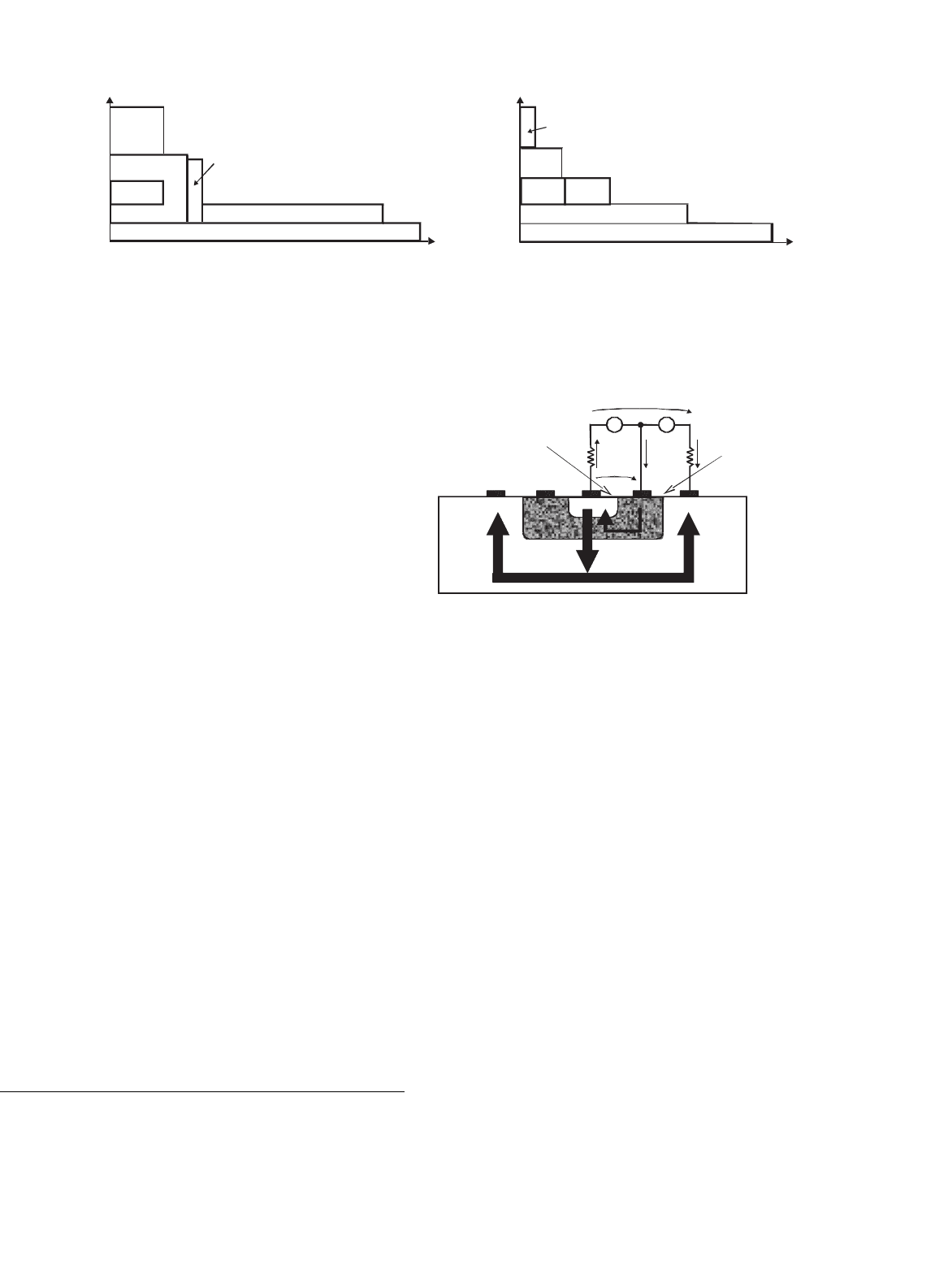
3.2 Basic Structure and Operation
The bipolar junction transistor (BJT) consists of a three-region
structure of n-type and p-type semiconductor materials, it
P
holes
flow
+
_
+
_
NN
electrons
injection
v
CE
v
BE
i
E
i
C
i
B
Reverse-biased
junction
Forward-biased
junction
BaseEmitter Collector
FIGURE 3.2 Structure of a planar bipolar junction transistor.
can be constructed as npn as well as pnp. Figure 3.2 shows
the physical structure of a planar npn BJT. The operation is
closely related to that of a junction diode where in normal
conditions the pn junction between the base and collector
is forward-biased (V
BE
> 0) causing electrons to be injected
from the emitter into the base. Since the base region is thin,
the electrons travel across arriving at the reverse-biased base–
collector junction (V
BC
< 0) where there is an electric field
(depletion region). Upon arrival at this junction the electrons
are pulled across the depletion region and draw into the col-
lector. These electrons flow through the collector region and
out the collector contact. Because electrons are negative carri-
ers, their motion constitutes positive current flowing into the
external collector terminal. Even though the forward-biased
base–emitter junction injects holes from base to emitter they
do not contribute to the collector current but result in a net
current flow component into the base from the external base
terminal. Therefore, the emitter current is composed of those
two components: electrons destined to be injected across the
base–emitter junction, and holes injected from the base into
the emitter. The emitter current is exponentially related to the
base–emitter voltage by the equation:
i
E
= i
E0
(e
V
BE
/ηV
T
−1) (3.1)
3 Power Bipolar Transistors 29
where i
E
is the saturation current of the base–emitter junction
which is a function of the doping levels, temperature, and the
area of the base–emitter junction, V
T
is the thermal voltage
Kt/q, and η is the emission coefficient. The electron current
arriving at the collector junction can be expressed as a fraction
α of the total current crossing the base–emitter junction
i
C
= αi
E
(3.2)
Since the transistor is a three terminals device, i
E
is equal
to i
C
+i
B
, hence the base current can be expressed as the
remaining fraction
i
B
= (1 −α)i
E
(3.3)
The collector and base currents are thus related by the ratio
i
C
i
B
=
α
1 −α
= β (3.4)
The values of α and β for a given transistor depend primar-
ily on the doping densities in the base, collector, and emitter
regions, as well as on the device geometry. Recombination
and temperature also affect the values for both parame-
ters. A power transistor requires a large blocking voltage in
the off state and a high current capability in the on state,
and a vertically oriented four layers structures as shown in
Fig. 3.3 is preferable because it maximizes the cross-sectional
area through which the current flows, enhancing the on-state
resistance and power dissipation in the device. There is an
intermediate collector region with moderate doping, the emit-
ter region is controlled so as to have an homogenous electrical
field.
Optimization of doping and base thickness are required to
achieve high breakdown voltage and amplification capabilities.
P
Base Emitter
Collector
N
+
N
+
N
-
FIGURE 3.3 Power transistor vertical structure.
Power transistors have their emitters and bases interleaved to
reduce parasitic ohmic resistance in the base current path and
also improving the device for second breakdown failure. The
transistor is usually designed to maximize the emitter periph-
ery per unit area of silicon, in order to achieve the highest
current gain at a specific current level. In order to ensure those
transistors have the greatest possible safety margin, they are
designed to be able to dissipate substantial power and, thus,
have low thermal resistance. It is for this reason, among others,
that the chip area must be large and that the emitter periphery
per unit area is sometimes not optimized. Most transistor
manufacturers use aluminum metalization, since it has many
attractive advantages, among these are ease of application by
vapor deposition and ease of definition by photolithography.
A major problem with aluminum is that only a thin layer can
be applied by normal vapor deposition techniques. Thus, when
high currents are applied along the emitter fingers, a voltage
drop occurs along them, and the injection efficiency on the
portions of the periphery that are furthest from the emitter
contact is reduced. This limits the amount of current each
finger can conduct. If copper metalization is substituted for
aluminum, then it is possible to lower the resistance from the
emitter contact to the operating regions of the transistors (the
emitter periphery).
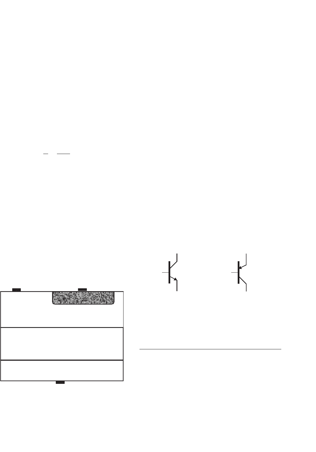
From a circuit point of view, the Eqs. (3.1)–(3.4) are used
to relate the variables of the BJT input port (formed by base
(B) and emitter (E)) to the output port (collector (C) and
emitter (E)). The circuit symbols are shown in Fig. 3.4. Most of
the power electronics applications use npn transistor because
electrons move faster than holes, and therefore, npn transistors
have considerable faster commutation times.
Base
Emitter
Collector
Base
Emitter
Collector
(a) (b)
FIGURE 3.4 Circuit symbols: (a) npn transistor and (b) pnp transistor.
3.3 Static Characteristics
Device static ratings determine the maximum allowable lim-
its of current, voltage, and power dissipation. The absolute
voltage limit mechanism is concerned to the avalanche such
that thermal runaway does not occur. Forward current rat-
ings are specified at which the junction temperature does not
exceed a rated value, so leads and contacts are not evapo-
rated. Power dissipated in a semiconductor device produces