Litton C.W., . Reynolds D.C., Collins T.C. Zinc Oxide Materials for Electronic and Optoelectronic Device Applications
Подождите немного. Документ загружается.

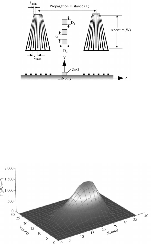
To determine the light field distribution, the response curves from each individual active
area are first constructed to form the standard curves. Under UV illumination, the SAW
insertion loss responses were then interpolated from the standard curves to deduce the light
power intensity. The frequency shift is insignificant due to the photoelectric effect in the
SFIT SAW device. From the insertion loss evaluation, a UV photosensitivity of 65 mW
cm
2
at 380 nm was achieved with a minimum optically active area of 0.04 mm
2
.
The corresponding insertion loss difference is 58.33 dB. Figure 11.25 shows the
Figure 11.24 Schematic diagram of a hybrid ZnO/LiNbO
3
SAW UV array photodetector.
Three ZnO active areas are shown by the squares in the top view. Reprinted from C. Ma, T.
Huang, and J. Yu, Application of slanted finger interdigital transducer surface acoustic wave
devices to ultraviolet array photodetectors, J. Appl. Phys., 104, 033528 (2008)
Figure 11.25 Measured light field distribution using a hybrid ZnO/LiNbO
3
SAW UV array
photodetector. Reprinted from C. Ma, T. Huang, and J. Yu, Application of slanted finger
interdigital transducer surface acoustic wave devices to ultraviolet array photodetectors, J.
Appl. Phys., 104, 033528. Copyright (2008) with permission from American Institute of Physics
ZnO Film-Based UV Photodetectors 313
measured light field distribution at a UV wavelength of 380 nm from an SFIT SAW device
with three ZnO active areas (Figure 11.24).
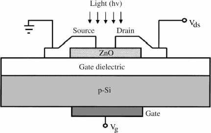
11.3.4 Photodetectors Using ZnO TFT
A field-effect phototransistor is a three terminal device in which photodetection occurs due
to photogenerated carriers in the semiconduct or channel upon optical excitation and the
presence of an electric field at the semiconductor and the gate oxide interface for the
carrier extraction. ZnO TFT is an optically transparent field-effect transistor primarily used
for display technology. Figure 11.26 shows the schematic diagram of a bottom-gate ZnO-
based TFT optical detector structure.
The ZnO channel layer is used as a photoconductor, where photogenerated carriers are
collected by source and drain electrodes. The gate electrode is separated from the active
channel layer through a layer of gate dielectric (e. g. SiO
2
). By control of the voltage applied
to the gate electrode, the charge density in the channel and the source-to-drain conductance
are changed through formation of a space charge layer in the channel. For the n-channel ZnO
TFT device, a positive gate voltage increases the electron density in the channel, while a
negative gatevoltage decreases the electron density. As a result, a photoconductive gain in the
phototransistor is modulated by varying the gate voltage. The TFT-based phototransistors
offer the advantages of high photoconductive gain, a large current transfer ratio, and
versatility in designing the optically controlled circuits (e.g. photoinverter, photodetector,
and opto-isolator, etc.). The photocurrent in the TFT is proportional to the gate voltage.
ZnO TFT-based optical detectors were reported by Bae et al.
[87,88]
ZnO TFTs were
fabricated using the RF-magnetron sputtering technique at room temperature or at 300
C
for the ZnO channel layer. RF sputtering is chosen due to its capability of low temperature
deposition, low cost, and convenience in fabrication. A wide range of materials were
selected for the source and drain electrodes of the ZnO TFTs. These include Al, Au, Ti and
transparent oxides (NiO
x
), etc. p-Si and glass are used as the substrates. On Si substrates,
thermally grown SiO
2
provides high quality gate dielectric. A poly-4-vinylphenol (PVP)
polymer gate dielectric was also demonstrated.
[89]
The optical response of TFTs shows
Figure 11.26 Schematic structure of a bottom-gate ZnO-based TFTTFT optical detector.
Adapted from H. S. Bae, et al., Photodetecting properties of ZnO-based thin-film transistors,
Appl. Phys. Lett. 83, 5313. Copyright (2003) with permission from American Insitute of Physics
314 ZnO-Based Ultraviolet Detectors

high gain in UV wavelength (340 nm), as well as in blue (450 nm) and green (540 nm)
wavelengths. The dynamic UV response of TFTs was measured to be 300 ms. All
indicate that the elimination of mid gap states in the sputtered ZnO channel is critically
important for improving the photodetection properties of TFTs. The UV photosensitivity
is dramatically enhanced when the TFT is operated under the depletion mode with a
negative gate bias instead of the accumul ation mode with a positive gate bias. This is due
to reduction of dark current in the ZnO channel under the depletion mode.
11.3.5 Mg
x
Zn
1x
O UV Photodetector
There is keen interest in the solar blind UV photodetectors, which find broad applications
in space engineering, flame detection, and biotechnology. ZnO can alloy with MgO to
form the ternary compound Mg
x
Zn
1x
O to extend the energy band gap, and therefore the
detection spectrum into the shorter wavelength region. The direct energy band gap of
wurtzite-structured Mg
x
Zn
1x
O can be tuned from 3.3 (x ¼0) to 4.0 eV (x ¼0.34),
corresponding to a cut-off wavelength from 375 to 305 nm. Further increase of Mg
composition would extend the indirect band gap of cubic-structured Mg
x
Zn
1x
Oupto
7.8 eV. Difficulties for the growth of high quality Mg
x
Zn
1x
O films are partly from the fact
that MgO (cubic) and ZnO (hexagonal) have different crystal structures. According to the
phase diagram, the solid solubility of Mg in hexagonal ZnO is less than 4%. However, by
using nonequilibrium growth methods, high quality wurtzite Mg
x
Zn
1x
O films with up to
34% Mg incorporation have been achieved without phase segregation.
The energy band gap of Mg
x
Zn
1x
O follows Vegard’s law:
E
g
ðMg
x
Zn
1x
OÞ¼ð1xÞE
g
ðZnOÞþxE
g
ðMgOÞð11:22Þ
Figure 11.27 shows the energy band gap of Mg
x
Zn
1x
O as a function of Mg composi-
tion. It is shown that the Mg
x
Zn
1x
O films have wurtzite and cubic crystal structures for
Figure 11.27 Band gap energy of Mg
x
Zn
1x
O films as a function of Mg composition. Reprinted
from W. Yang, et al., Compositionally-tuned epitaxial cubic Mg
x
Zn
1x
O on Si(100) for deep
ultraviolet photodetectors Appl. Phys. Lett. 82, 3424. Copyright (2003) with permission from
American Institute of Physics
ZnO Film-Based UV Photodetectors 315
Mg composition G37% and H62%, respectively. For Mg composition between 37% and
62%, a mixed hexagonal and cubic phase occurs.
Yang et al.reportedthefirstMg
x
Zn
1x
O MSM photoconductive detector grown by
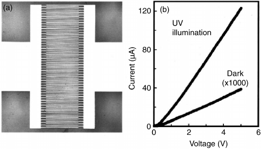
PLD on c-plane sapphire substrates.
[91]
Shown in Figure 11.28(a) i s an optical
microscope image of a Mg
0.34
Zn
0.66
O UV detector with a size of 250 1000 mm
2
.
The IDT metal electrodes are 250 mmlong,5mm wide, and have an interelectrode
spacing of 5 mm. A 150 nm thick Cr/Au bilayer was patterned as the metal contacts by
conventional photolithography and ion milling. To achieve ohmic contact, a thin layer
(3 nm) of chromium was u sed. A monochromator (150 W xenon lamp, 1200 lines
mm
1
grating) and a nitrogen gas laser (337.1 nm, pulse duration 4ns) were used as
the excitation source to characterize the Mg
0.34
Zn
0.66
O detector. Figure 11.28(b) shows
the linear relationship of t he I–V curves for both dark current and photocurrent. At 5 V
bias, the dark current and photocurrent under UV illumination (308 nm, 0.1 mW) are
40 nA and 124 mA, respect ively, indicating a responsivity of 1200 AW
1
. The visible
rejection (R 308 nm/R 400 n m) is more t han four orde rs of m ag nitu de .
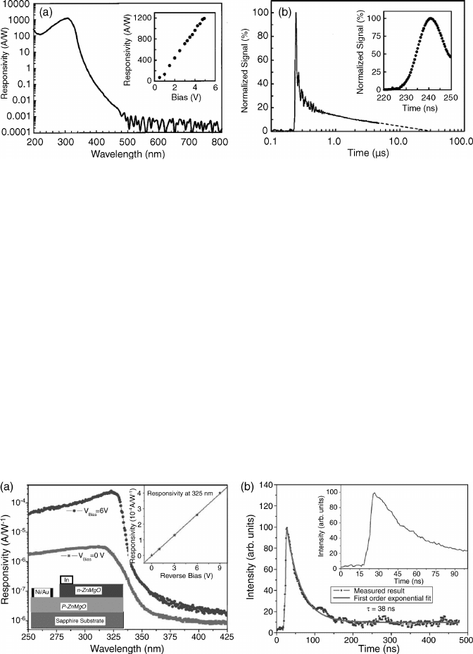
The spectra response of a Mg
0.34
Zn
0.66
O UV detector under illumination is plotted in
Figure 11.29(a). The peak response is at 308 nm. The3 dB cut-off wavelength is 317 nm.
The inset of Figure 11.29(a) is the responsivity as a function of bias voltage. A linear
relationship was obta ined between 0.5 V and 5 V, indicating no carrier mobility saturation
or sweep-out effect up to the applied bias. Figure 11.29(b) shows the temporal response of
an Mg
0.34
Zn
0.66
O UV detector with 3 V bias and 50 W load. The 10–90% rise and fall time
are 8 ns and 1.4 ms, respectively. The signal drops to zero at 30 ms.
A prototype deep UV detector based on cubic-phase Mg
x
Zn
1x
O thin films was
demonstrated for solar-blind detection.
[90]
To reduce the lattice mismatch between the
film and the substrate, a thin SrTiO
3
buffer layer was used to grow Mg
x
Zn
1x
O(x H 0.62)
on Si (100) substrates by PLD. The epitaxial relationship was established as Mg
x
Zn
1x
O
(100)//SrTiO
3
(100)//Si(100) and Mg
x
Zn
1x
O[100]//SrTiO
3
[100]//Si[100]. The Mg
x
Zn
1x
O
Figure 11.28 (a) Optical microscope image of a Mg
0.34
Zn
0.66
O MSM UV detector. The Cr/Au
fingers are 250 mm long, 5 mm wide with an interfinger spacing 5 mm. (b) I–V characteristicsof dark
current and photocurrent under 308 nm, 0.1 mW UV light illumination. Reprinted from W. Yang,
et al., Ultraviolet photoconductive detector based on epitaxial Mg
0.34
Zn
0.66
O thin films, Appl.
Phys. Lett. 78, 2787. Copyright (2001) with permission from American Institute of Physics
316 ZnO-Based Ultraviolet Detectors
photodetector with MSM structure was fabricated. The IDT metal electrodes (250 m m long,
5 mm wide, with 5 mm spacing) were patterned from a 250 nm gold film, followed by rapid
thermal annealing at 400
C. A peak photoresponsivity was achieved at 225 nm.
Liu et al. reported a Mg
x
Zn
1x
O p-n homojunction diode grown on c-plane sapphire by
plasma-assisted MBE.
[92]
The spectra response of a Mg
0.24
Zn
0.76
O p-n photodiode under
the reverse bias of 0 and 6 V is plotted in Figure 11.30(a). The left inset of Figure 11.30(a)
shows the schematic diagram of the Mg
x
Zn
1x
O p-n photodiod e structure. The cut-off
wavelength is 345 nm, corresponding to 24% Mg incorporation. The visible rejection
ratio (R 325 nm/R 400 nm) achieved is four orders of magnitude under 6 V reverse bias.
The peak responsivity at 325 nm is 4 10
4
AW
1
at 9 V reverse bias. A linear relationship
Figure 11.30 (a) Spectral response of a Mg
0.24
Zn
0.76
O p-n photodiode under the reverse bias
of 0 and 6 V. The left inset of shows the schematic diagram of the Mg
0.24
Zn
0.76
O p-n
photodiode. The right inset shows the responsivity at 325 nm vs reverse bias voltage. (b)
Transient response of the Mg
0.24
Zn
0.76
O p-n photodiode excited by a 266 nm Nd:YAG laser
with a 50 O load. The inset shows the enlarged pulse response. Reprinted from K. W. Liu, et al.,
Zn
0.76
Mg
0.24
O homojunction photodiode for ultraviolet detection, Appl. Phys. Lett. 91,
201106 (2007)
Figure 11.29 (a) Spectral response of a Mg
0.34
Zn
0.66
O detector at 5 V bias. The inset shows
the responsivity as a function of bias voltage under 308 nm, 0.1 mW UV light illumination. (b)
Temporal response of a Mg
0.34
Zn
0.66
O detector excited by nitrogen gas laser pulses. The inset
shows the enlarged pulse response. Reprinted from W. Yang, et al., Ultraviolet photoconduc-
tive detector based on epitaxial Mg
0.34
Zn
0.66
O thin films, Appl. Phys. Lett. 78, 2787. Copyright
(2001) with permission from American Institute of Physics
ZnO Film-Based UV Photodetectors 317
is obtained between 0 V and 9 V, indicating no carrier mobility saturation up to 9 V.
Figure 11.30(b) shows a transient response of the Mg
0.24
Zn
0.76
O p-n photodiode under the
excitation of 266 nm from a Nd:YAG laser with a 50 W load. The photodiode has fast
photoresponse with a rise time of 10 ns and fall time of 150 ns. The thermal limited
detectivity was calculated as 1.8 10
10
cm Hz
1/2
W
1
at 325 nm with a noise equivalent
power of 8.4 10
12
WHz
1/2
at room temperature.
11.4 ZnO NW UV Photodetectors
One-dimensional ZnO nanostructures have attracted increasing attention due to their
promising optical and electrical properties. The electron–hole interaction will have orders
of magnitude enhancement in a nanostructure, due to the dramatically increased electronic
density of states near the van Hove singularity. Bulk ZnO has a small exciton Bohr radius
(1.8–2.3 nm).
[93,94]
The quantum confinement effect in ZnO NWs is observable at the scale
of an exciton Bohr radius. On the other hand, the giant oscillator strength effect occurs in
ZnO NWs with diameters larger than the bulk exciton Bohr radius but smaller than the
optical wavelength,
[95,96]
making ZnO NWs suitable for high sensitivity UV detection.
Single crystalline ZnO NWs haven been synthesized by various techniques, such as
MOCVD,
[97–99]
CVD,
[100,101]
chemical vapor transport and condensation (CVTC),
[102,103]
catalyst-assisted MBE,
[104]
template-assisted growth
[105]
and solution-based synthe-
sis.
[106]
ZnO NWs have the same lattice constants and crystal structure of bulk, confirmed
by XRD and TEM data.
[94,107]
Many bulk properties are still preserved in ZnO NWs. In
comparison with its bulk counterpart, ZnO nanostructures possess certain significant
characteristics for UV detection, including: (i) high surface-to-volume ratio and large
density of surface trap states (primarily oxygen-related hole traps) greatly increase the
photogenerated carrier lifetime and modify the effective carrier mobility; and (ii) reduced
dimension decreases the carrier transit time in the active area of the nanoscale device. As
a result, a large photoconductive gain is expected. A photoconductive gain as high as 10
8
was reported in a ZnO single NW UV photodetector,
[101]
which is promising for single-
photon detection.
In general, there are two types of device configurations of ZnO NW photodetectors: (i) a
vertical structure prepared by self-assembled growth or template-assisted growth; and (ii)
a horizontal structure, in which ZnO nanostructure photodetectors are fabricated using the
“pick-and-place” manipulation of randomly dispersed ZnO NWs. In the latter, ZnO NWs
are usually scratched from the growth substrate, then sonicated in an organic liquid drop
and dispersed onto a template. After picking up an appropriate single NW, metal contacts
are deposited on both ends of the NW using photo- or nanolithography. Most horizontal
devices are randomly located on the template surface, and then the photoconduction
properties of ZnO NWs are characterized and studied.
11.4.1 Photoconductive Gain in a ZnO NW
11.4.1.1 Theoretical Background
A simplified approach to evaluate the carrier transport and photoconduction in an
individual ZnO NW is based on classical principles governing the carrier generation and
318 ZnO-Based Ultraviolet Detectors

transport in semiconductors, providing that many bulk properties are still kept in the ZnO
NW. The key factors for modeling a ZnO NW device are all surface-related, including
surface state modified carrier mobility and carrier lifetime. A single ZnO NW photode-
tector was modeled by Prades et al.,
[108]
as an arbitrary volume of length L , width W, and
thickness T, which is illustrated in Figure 11.31.
The current density in the NW follows the classical rule:
j
ph
¼ qDn
ph
v ð 11 :23Þ
where q is the elemental charge, Dn
ph
is the photogenerated carrier density and v is the
velocity of the carriers. By assuming a constant carrier generation profile within the optical
absorption depth a
1
, Dn
ph
is expressed by:
Dn
ph
¼
hF
V
ph
tðFÞ¼
hF
a
1
WL
tðFÞð11:24Þ
where h is the quantum efficiency, F is the photon absorption rate, V
ph
is the photo-
generation volume (Figure 11.31), a is the optical absor ption coefficient and t is the carrier
lifetime, which is a function of photon absorption rate F. The continuity equation gives:
@Dn
ph
@t
¼ g
ph
Dn
ph
tðFÞ
ð11:25Þ
where g
ph
is the carrier photogeneration rate.
Figure 11.31 Schematic of a NW structure with an arbitrary volume of length L, width W and
thickness T, under a photon flux F
ph
. Free carriers are optically generated within an absorption
depth a
1
, leading to a photocurrent density j
ph
. Reprinted from J. D. Prades, et al., Toward a
Systematic Understanding of Photodetectors Based on Individual Metal Oxide Nanowires,
J. Phys. Chem. C, 112, 14639 (2008)
ZnO NW UV Photodetectors 319

Case 1: Surface Modified Carrier Mobility. If the photogenerated excess carrier density
is independent of the carrier lifetime, the time dependent photocurrent can be derived from
Equation (11.25):
i
ph
ðtÞ¼I
ph
ð1e
t=t
r
Þð11:26Þ
i
ph
ðtÞ¼I
ph
e
t=t
f
ð11:27Þ
where I
ph
is the steady-state photocurrent, t
r
is the photocurrent rise time and t
f
is the
photocurrent fall time. When an external electric field is applied along the length direction,
the carrier drift velocity is related to the applied voltage V by:
v ¼ m
*
E ¼
m
*
V
L
ð11:28Þ
where m
is the effective carrier mobility. It consists of contributions from the bulk (m
B
)
and the surface (m
S
):
1
m
*
¼
1
m
B
þ
1
m
S
ð11:29Þ
The photocurrent in the NW is derived as:
I
ph
¼ j
ph
ða
1
WÞ¼q
W
L
bhtm
*
VF
ph
ð11:30Þ
where b is the fraction of photons not reflected by the surface and F
ph
is the incident
photon flux. The photoconductive gain G
ph
is defined as the ratio between the number of
electrons collected and the number of photons absorbed per unit time:
G
ph
¼
I
ph
qF
1
L
2
htm
*
V ð11:31Þ
Case 2: Surface Modified Carrier Lifetime. In the second case, carrier lifetime is treated
as a function of photon absorption rate due to the presence of high density surface trap states.
Figure 11.32 illustrates the photoconduction process in a single ZnO NW photodetector.
Similar to the oxygen adsorption–photod esorption process described in Section 11.2, the
hole-trapping mechanism through the surface states (such as dangling bonds at the surface)
governs the photoconduction in ZnO NWs. Under illumination with photon energy higher
than the energy band gap, electron–hole pairs are generated [Figure 11.32(a)]. Holes migrate
to the surface along the potential field provided by the band bending [Figure 11.32(b)] and
dischargeof thenegativelycharged adsorbedoxygenions , andaretrapped at thesurfacestates
[Figure 11.32(c)]. The unpaired electrons are either collected at the anode or recombine with
holes generat ed when oxygen is readsorbed at the surface.
Soci et al. developed a model to describe the internal photoconductive gain in
semiconductor NWs, where the high density of surface trap states enhances the carrier
lifetime, leading to photoconductive gain.
[101]
When surface hole traps are filled by the
photogenerated holes upon illumination, the depletion region near the surface becomes
narrow and the band bending is flattened. This increases the free hole concentration and
the probability of electon–hole recombination. The carrier lifetime is a function of photon
320 ZnO-Based Ultraviolet Detectors
absorption rate:
tðFÞ¼t
0
1
1 þðF=F
0
Þ
n
ð11:32Þ
where t
0
is the carrier lifetime at low excitation and F
0
is the photon absorption rate when
trap saturation occurs. Assuming the photoabsorption occurs in the entire ZnO NW, from
Equations (11.24) and (11.32), the photocurrent in the NW is given by:
I
ph
¼ qDn
ph
vA ¼ qhð
t
0
t
t
Þ
F
1 þðF=F
0
Þ
n
ð11:33Þ
where n is the carrier drift velocity and t
t
is carrier transit time. The photoconduc tive gain
G
ph
is derived from Equation (11.33):
G
ph
¼
I
ph
qF
¼
t
0
t
t
h
1 þ F=F
0
ðÞ
n
ð11:34Þ
The gain–bandwidth (3 dB bandwidth) product of the NW photodetector is obtained by:
G
ph
B ¼
1
2pt
t
1
1 þðF=F
0
Þ
n
ð11:35Þ
11.4.1.2 Experimental Results
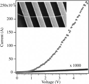
Large photoconductivity of a single ZnO NW was first reported by Kind et al. in 2002.
[22]
Single crystalline ZnO NWs with diameters ranging from 50 to 300 nm were dispersed on
prefabricated gold electrodes. Electrical resistivities without and with UV light irradiation
were measur ed in a four-terminal configuration. The conductivity of ZnO NW under UV
irradiation increases by four to six orders of magnitude compared with the dark current
with a response time in the order of seconds (Figure 11.33). The photoresponse has a cut-
off wavelength of 370 nm. The slow process can be suppressed by reducing the trap
Figure 11.32 (a) Photoconduction in a single NW photodetector. (b, c) Surface trapping and
photoconduction mechanism in a ZnO NW: (b) in the dark; and (c) under optical excitation.
Reprinted from C. Soci, et al., ZnO Nanowire UV Photodetectors with High Internal Gain,
Nano Lett 7, 1003. Copyright (2007) with permission from American Chemical Society
ZnO NW UV Photodetectors 321
density and background carrier concentration. ZnO NWs also show a reversible switching
behavior between dark conductivity and photoconductivity when the UV lamp is turned on
and off. This suggests that ZnO NWs are good candidates for optoelectronic switches.
The photoconduction properties of ZnO NW photodetectors are controlled by the
geometrical size of the NWs and electrodes, ambient gas, and surface coatings. The
electron mobility in ZnO varies depending on the diameter of the NWs. For example,
mobility values of 2–30 cm
2
V
1
s
1
were reported for NWs with radii G100 nm,
[109–111]
and 200 cm
2
V
1
s
1
in thicker NWs.
[101]
By surface passivation of the ZnO NWs,
electron mobility up to 1000 cm
2
V
1
s
1
was reported.
[111–114]
Photoconduction was investigated in the ZnO NWs which were grown by CVD, with
diameters of 150–300 nm and lengths of 10–14 mm.
[101]
After the NWs were transferred
onto a SiO
2
/Si substrate, Ti/Au electrodes were patterned on top of these NWs using
photolithography for photocurrent detection. Figure 11.34(a) shows the photocurrent
spectra of an array of ZnO NWs. The photoresponsivity of ZnO NWs increases by about
two orders of magnitude after keeping the sample under vacuum (10
4
Torr) for about
20 min. This is consistent with the increased carrier lifetime caused by a reduced oxygen
readsorption rate in vacuum. Figure 11.34(b) plots the photoconductive gain from
Equation (11.34). A high internal photoconductive gain of 2 10
8
is obtained, corre-
sponding to a gain–bandwidth product of 6 GHz. The intrinsic material parameters of ZnO
NWs are also estimated based on the experimental results. An intrinsic carrier concentra-
tion as low as 10
13
cm
3
and high electron mobility of 270 cm
2
V
1
s
1
are achieved.
These material data obtained from the ZnO NW are much better than ZnO thin films,
indicating a low bulk defect density in the NW.
Surface functionalization and passivation are used to dramatically improve the photo-
responsitivity of ZnO nanostructures.
[114,115]
It was found that a single ZnO nanobelt
coating with a thin layer (20 nm) of plasma polymerized acrylonitrile (PP-AN) showed
Figure 11.33 I–V characteristics of dark current and photocurrent of a single ZnO NW under
365 nm, 0.3 mW cm
2
UV light illumination. The inset is a field emission scanning electron
microscopy (FESEM) image of a ZnO NW with 60 nm diameter bridging four Au electrodes.
Reprinted from H. Kind, H. Yan, et al., Adv. Mater, 14, 158. Copyright (2002) with permission
from John Wiley and Sons
322 ZnO-Based Ultraviolet Detectors