Litton C.W., . Reynolds D.C., Collins T.C. Zinc Oxide Materials for Electronic and Optoelectronic Device Applications
Подождите немного. Документ загружается.

J
o
¼2.38 10
8
Acm
2
were obtained from curve fitting. The barrier height F
B
is estimated
to be about 0.84 eV by using A
32 A cm
2
K
2
(A
*
¼ 4pqm
*
k
2
h
3
, where m
0.27m
0
).
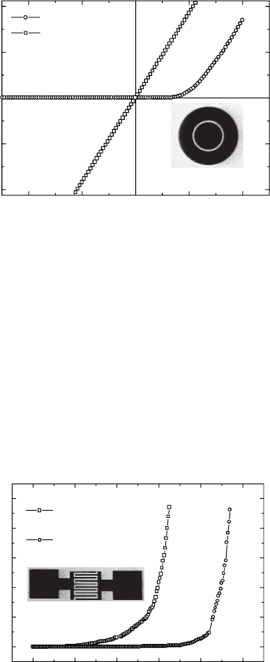
At a reverse bias of 1 V, the leakage current (0.1 nA) of the Ag-ZnO-Al device is about five
orders of magnitude smaller than that of the Al-ZnO-Al device (10 mA).
The Ag-ZnO-Ag MSM structure with IDT configuration was used to evaluate the UV
detector performance. Figure 11.14 shows the dark and photoilluminated I–V character-
istics of a Schottky detector. The wavelength and power of the illuminated light are 368 nm
and 0.1 mW, respectively. The leakage current of the photodetector is about 1 nA at a bias
of 5 V. The breakdown starts at about 8 V. The early and soft breakdown is mainly due to
1086420
0.0
0.2
0.4
0.6
0.8
1.0
Photoilluminated
λ
=368 nm, W=0.1
μ
W
Dark
Current (
μ
A)
Voltage (V)
Figure 11.14 I–V characteristics of a ZnO Schottky photodetector with an IDT structure. The
inset shows a SEM picture of the top view of the device. Reprinted from S. Liang, et al., ZnO
Schottky ultraviolet photodetectors, J. Cryst. Growth, 225, 110. Copyright (2001) with
permission from Elsevier
1.00.50.0-0.5-1.0
-8
-4
0
4
8
Electrode Gap = 10
μ
μ
m
Ag-ZnO-Al
Al-ZnO-Al
Current (
μ
A)
Voltage (V)
Figure 11.13 I–V characteristics of ZnO diodes with circular pattern. The electrode gap is
10 mm. Reprinted from S. Liang, et al., ZnO Schottky ultraviolet photodetectors, J. Cryst.
Growth, 225, 110. Copyright (2001) with permission from Elsevier
ZnO Film-Based UV Photodetectors 303
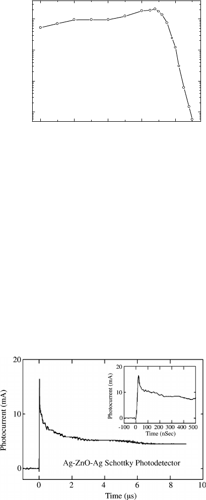
the nonuniform field distribution, especially at the corners of the finger electrodes in the
IDT patterns. The low-frequency photoresponsivity is about 1.5 AW
1
, which corresponds
to a quantum efficiency of 2.5. We believe that the photoconductive effect that occurs at
the high field contributes to the large gain (H1).
The spectral photoresponse of a IDT Schottky device is shown in Figur e 11.15. The
photoresponsivity drops more than three orders of magnitude from 370 to 390 nm.
The sharp cut-off at wavelength of 370 nm agrees with the ZnO energy band gap of
3.35 eV. The responsivity decreases at the shorter wavelength range due to decrease of the
penetrating depth of the light, resulting in an increase of the surface recombination.
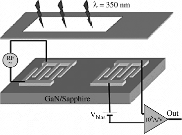
Figure 11.16 shows photocurrent as a function of time from an IDT ZnO Schottky
detector. The photoresponse has a fast component, which rises within 12 ns and falls to
66% of its peak value within 50 ns, as shown in the inset of Figure 11.16. After that a slow
380360340320300
10
-3
10
-2
10
-1
10
0
Ag-ZnO-Ag Schottky Photodetector
Responsivity (a.u.)
Wavelen
g
th (nm)
Figure 11.15 Spectral response of a ZnO Schottky photodetector with an IDT structure.
Reprinted from S. Liang, et al., ZnO Schottky ultraviolet photodetectors, J. Cryst. Growth, 225,
110. Copyright (2001) with permission from Elsevier
Figure 11.16 Transient photocurrent of a ZnO Schottky photodetector with an IDT structure
under a nitrogen gas laser pulsed excitation. The inset is a magnified response pulse. Reprinted
from S. Liang, et al., ZnO Schottky ultraviolet photodetectors, J. Cryst. Growth, 225, 110.
Copyright (2001) with permission from Elsevier
304 ZnO-Based Ultraviolet Detectors

process follows lasting about 5 ms (not shown in the figure). The fast response in a MSM
detector is usually related to the transit time of the photogenerated carriers, while the slow
response in a ZnO MSM detector is usually attributed to the oxygen adsorption at the
surface and grain boundaries.
[15,40]
The high quality epitaxial ZnO films were used for
both Schottky and photoconductive detectors. Such a slow process was not observed in the
photoconductive devices with the same material quality. Therefore, this slow process was
attributed to the trapping and emission of photogenerated carriers in the ZnO surface of the
Schottky detector. It should be noted that oxygen plasma was used to treat the ZnO surface
only when making the Schottky detectors.
Table 11.2 summarizes the main device parameters for ZnO Schottky-type MSM
photodetectors with various metal contact electrodes reported by Young et al.
[76–79]
As
shown in Table 11.2, the UV responsivity, quantum efficiency, and noise spectra were
studied and compared in the ZnO Schottky-type MSM UV detectors with various metal
contact schemes. ZnO epitaxial films were grown on the c-plane sapphire substrate using
plasma-assisted MBE. Room temperature Hall measurements showed the carrier concen-
tration and mobility of as-grown ZnO films were 1.71 10
16
cm
3
and 26.4 cm
2
V
1
s
1
,
respectively. Schottky-type MSM photodetectors were made of IDT Schottky contacts
deposited on top of a ZnO active layer. To form Schottky contact to ZnO, metals with large
work functions are chosen, including Ag, Pd, Ni, and Ru. Depending on the ZnO-based
material quality and surface conditions, the reported data vary from different research
groups.
11.3.3 Integrated Surfac e Acoustic Wave and Photoconductive Wireless
UV Detectors
11.3.3.1 The Principle of UV SAW Devices
Most UV photodetectors use either voltage or current as the output. In order to construct
zero-power and wirel ess UV detector for applications such as distributed sensor network,
UV-SAW photodetectors have been proposed based on acoustoelectric interaction.
[80–82]
In the UV-SAW photodetectors, the UV sensitive semiconductor layer is integrated with
the SAW device built on the piezoel ectric material. The incident light will be absorbed by
the semiconductor and generate electron–hole pairs. These free carriers in the semic on-
ductor layer will interact with the electri c field accompanying the propagating SAW in the
piezoelectric material, resulting in increase of insertion loss. Furthermore, a velocity
reduction will occur due to the piezoelectric stiffening, resulting in a phase shift and time
Table 11.2 Comparison of main device parameters of ZnO Schottky-type MSM
photodetectors with Ag, Pd, and Ni metal contacts
[76–79]
Metal Photoresponsivity
(A W
1
at 370 nm)
Quantum
efficiency
Noise equivalent
power (W)
a
Normalized
detectivity (Hz
1/2
W
1
)
Ag 0.066 17.3% 6.8 10
13
1.04 10
12
Pd 0.051 11.4% 1.13 10
12
6.25 10
11
Ni 0.09 23.8% 6.4 10
12
1.1 10
11
a
Measured at a given bandwidth of 100 Hz and an applied bias of 1 V.
ZnO Film-Based UV Photodetectors 305
delay across the SAW device. Both the attenuation and phase changes correlated with the
incident light intensity and wavelength can be used for the optical detection. The UV-SAW
photodetectors offer advantages of low power consumption (due to the passive nature) and
RF readout (for wireless communication).
Several UV-SAW photo detectors have been demonst rated with various piezoelectric
and UV sensing layer integration. GaN-based UV SAW devices were demonstrated by
using MOCVD grown GaN on c-plane sapphire substrates.
[80,81]
In these devices, GaN,
which is a weakly piezoelectric wide-band-gap semiconductor, is used for both SAW
excitation and UV sensing. A GaN-based SAW UV detector was reported to cause a
60 kHz oscillation frequency shift at 221.3 MHz when used as a delay element in the
feedback path of an oscillator. The estimated electromechanical coupling coefficient K
2
is
0.055% and the achieved relative oscillation frequency shift is 271 ppm. The maximum
response was observed at the optical wavelength of 365 nm, which corresponds to the
photon energy equal to the GaN band gap of 3.4 eV.
[80]
In an alternative configuration, a
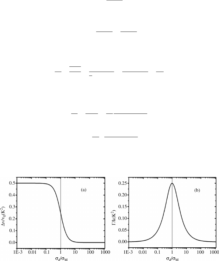
SAW launched from an input IDT transducer is used to sweep electron–hole pairs
generated in the sensing area to an MSM photoconductive detector out of the sensing
region (Figure 11.17).
[81]
The responsivity of this MSM photodetector is a function of the
frequency and power of the SAW. Based on the acoustoelectric interaction, the coupling
coefficient K
2
is the key factor to influence the change of velocity and attenuation.
A higher K
2
is desirable for a larger acoustoelec tric effect and hence a higher sensitivity.
In the case of a thin semiconducting layer system placed on the piezoelectric crystal’s
surface, the mobile carriers are confined to a conductive layer of thickness d, which is
assumed to be much smaller than the wavelength of the SAW. The thin semiconducting
layer can be a single layer semiconductor film under optical illumination. The longitudinal
electric field of the SAW can only be screened at the piezoel ectric surface, i.e. z ¼0, where
z is along the growth direction of the semiconductor thin film. The conductivity
modulation in a thin sheet layer results in an effective modification of the relaxation
frequency o
c
, which is a function of the SAW wave vector k; k ¼2p/l for the homoge-
neous semiconductor.
Figure 11.17 Schematic diagram of integration of SAW generator and a UV photodetector.
Reprinted from T. Palacios, et al., Proc. 2002 IEEE Ultrasonics Symp. 1, 55. Copyright (2002)
with permission from IEEE
306 ZnO-Based Ultraviolet Detectors
Because the electric field in the homogeneous bulk semiconductor decreases exponen-
tially with the height (e
kz
), a layer of thickness 1/k effectively carries this current. For the
thin semiconducting layer, the available thickness to carry the current is defined as d. Thus
the effective resistance and the time constant become 1/kd times larger:
t ¼
e
1
þe
2
s kd
ð11:16Þ
and the conductivity relaxation frequency o
c
is:
o
c
¼
kd s
e
1
þe
2
¼
s
d
k
e
1
þe
2
ð11:17Þ
where s
d
¼sd is the sheet conductivity of the thin film. Thus, the ratio o
c
/o becomes
frequency independent:
o
c
o
¼
s
d
k
e
1
þe
2
o
¼
s
d
o
k
ðe
1
þe
2
Þ
¼
s
d
v
0
ðe
1
þe
2
Þ
¼
s
d
s
M
ð11:18Þ
where s
M
¼v
0
(e
1
þe
2
) is the conductivity at which the maximum loss occurs. Now
Equation (11.18) becomes after separation of the real part and the imaginary part:
Dv
v
0
¼
vv
0
v
0
¼
K
2
2
1
1 þðs
d
=s
M
Þ
2
ð11:19Þ
G ¼
K
2
2
k
ðs
d
=s
M
Þ
1 þðs
d
=s
M
Þ
2
ð11:20Þ
The relationships of Equations (11.19) and (11.20) are plotted in Figure 11.18. Shown in
Figure 11.18(a) is the relative change Dv/v
0
¼(vv
0
)/v
0
of the sound velocity. Figure 11.18(b)
Figure 11.18 Change in sound velocity Dv/v
0
(a) and attenuation coefficient per unit wave
vector k (b) in units of effective coupling coefficient K
2
as a function of the ratio s
d
/s
M
. The thin
conducting layer is assumed to be located on top of the piezoelectric surface. Reprinted with
permission from J. Zhu
ZnO Film-Based UV Photodetectors 307
is the attenuation G per unit length, as a function of the sheet conductivity of the thin
semiconducting layer.
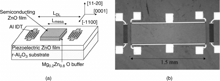
11.3.3.2 ZnO-Based Multilayer UV-SAW Photodetectors
Based on the acoustoelectric interaction, the device is designed by integrating a UV-
sensitive semiconducting ZnO layer with piezoelectric ZnO layer on r-Al
2
O
3
substrates.
The detailed bottom-up layer structure consists of a piezoelectric a-ZnO layer on r-Al
2
O
3
substrate for SAW generation, a Mg
0.2
Zn
0.8
O buffer layer, and a semiconducting ZnO
sensing layer [Figure 11.19(a)]. These three layers are all grown by MOCVD. A thick
piezoelectric ZnO film (2.0 mm) is first grown on r-Al
2
O
3
substrates. As ZnO has a lower
acoustic velocity than r-Al
2
O
3
, this layered system has dispersive acoustic velocity, with
higher order wave modes excited at higher film thickness–frequency (hf) products. Based
on the SAW simulation, the thickness is determined to ensure the excitation of the first
higher order Rayleigh wave mode, the Sezawa wave mode, in the test devices below
1.0 GHz. The Sezawa wave mode is chosen as it has higher acoustic velocity, v
SAW
, and
maximum effective piezoelectric coupling, K
eff
2
, than the base Rayleigh wave mode and
the Love wave mode. The as-grown, unintentionally doped MOCVD ZnO shows n-type
conductivity, with a carrier concentration of about 10
17
cm
3
. To compensate the excess
carriers in ZnO film and ensure efficient SAW excitation, the piezoelectric ZnO layer is
doped with Li to increase its resistivity to above 10
7
W cm. Then, a 50 nm thick
Mg
0.2
Zn
0.8
O buffer layer is used to isolate the semiconducting ZnO layer from the
piezoelectric ZnO layer and as a diffusion barrier for Li. The semiconducting ZnO layer’s
thickness, h
mesa
, varies from 200 to 400 nm to analyze the thickness dependence of the
SAW and optical responses. After the formation of the semiconducting ZnO sensing mesa
by wet chemical etching, the Al IDT transducers are deposited and patterned on top of the
piezoelectric ZnO surface. The top view of a prototype ZnO UV SAW device is shown in
Figure 11.19(b).
Figure 11.19 (a) Schematic structure of a ZnO-based multilayer UV-SAW device on r-Al
2
O
3
substrate. Reprinted from N. W. Emanetoglu, et al., Surface acoustic wave ultraviolet photo-
detectors using epitaxial ZnO multilayers grown on r-plane sapphire, Appl. Phys. Lett. 85,
3702 (2004) (b) Top view of the UV SAW device under an optical microscope. Reprinted with
permission from J. Zhu
308 ZnO-Based Ultraviolet Detectors
For the horizontal device structure, there are three main parameters: the SAW
wavelength l, the delay line length L, and the UV sensing mesa length L
mesa
. The SAW
wavelength l determines the operating frequency of the UV SAW device and is
determined by the periodicity of the IDT electrodes. Three wavelengths, 8, 12 and 16 mm,
are chosen based on the photolithography constra ints and the piezoelectric film thickness.
The aperture of the IDTs is chosen to be 380 mm. The ZnO UV SAW devices are
comprised of two sets, with delay lengths, L, of 1.2 mm and 1.7 mm, and corresponding
mesa lengths, L
mesa
, of 1.0 mm and 1.5 mm, respectively. Each set contains SAW devices
with 8, 12 and 16 mm acoustic wavelength. The length of the sensing mesa L
mesa
is chosen
based on ensuring sufficient phase shift and insertion loss change under UV illumination.
The devices are aligned parallel to the ZnO c-axis, which is in the surface plane of the
(11
20) ZnO film, to generate the Rayleigh type wave modes. In the IDT region, the base
Rayleigh wave mode has an estimated maximum coupling coefficient of 1.9% with a
velocity of 2768 m s
1
, while the maximum coupling coefficient for the Sezawa wave mode
is estimated to be 6% with an acoustic velocity of 5658 m s
1
, leading to a larger
photoresponse.
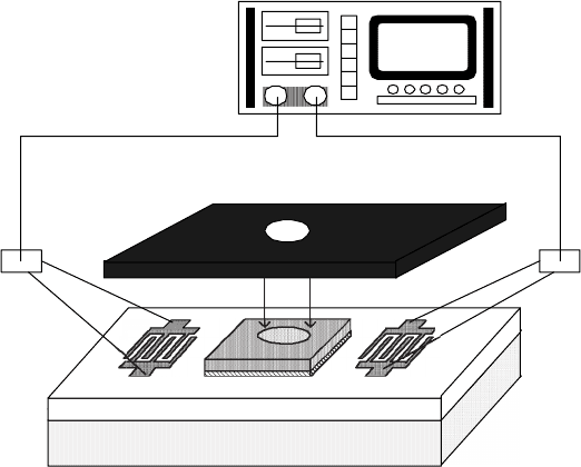
The ZnO SAW UV devices were tested using an HP 8753D network analyzer and
Cascade Microtech probes for the RF respo nse (th e transmission parameter S
21
). The ZnO
UV SAW device was first measured under the dark condition. A 75 W Xe lamp with a
monochromator system was used as the optical excitation source. Multiple UV filters were
used to adjust the power density of the incident light. Two optical illumination procedures
were used, illuminating the whole device surface and only illuminating the semiconduct-
ing ZnO mesa through a shadow mask, as shown in Figure 11.20. The light wavelengths
were varied from 630 to 300 nm. The light power density was varied from 810 mWcm
2
to
SAW Sensors
UV Light
Optical Window
Rack mount
HP 8753D Network Analyzer
Figure 11.20 Schematic of the UV-SAW testing set-up. Reprinted with permission from J. Zhu
ZnO Film-Based UV Photodetectors 309
2.32 mW cm
2
at l
light
¼365 nm. I–V measurements were used to determine the change in
the resistance of the mesa active layer as a function of the light wavelength and power, then
correlated with the SAW photores ponse.
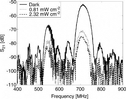
Figure 11.21 shows the SAW response of a UV SAW device with l
SAW
¼8 mm, L ¼1mm,
and h
mesa
¼300 nm, under dark and two different light power conditions (l
light
¼365 nm),
while using a shadow mask to limit the illuminated area to the mesa. The power density of the
incident light was adjusted by applying UV filters to the light beam. The base Rayleigh wave
mode response is at 545.9 MHz, with an insertion loss of67.8 dB. In comparison, the Sezawa
wave mode response is at 711.3 MHz, corresponding to v
SAW
¼5690 m s
1
, with an insertion
loss of52.5 dB. The Sezawa wave insertion loss increases to75.3 dB when the light power
is 2.32 mW cm
2
, while the Rayleigh wave insertion loss is83.3 dB. In comparison, the UV
SAW detector with a 200-nm-thick active region had an insertion loss of 33.8 dB for the
Sezawa wave mode, due to its lower conductance. The insertion loss can also be improved by
using better designed IDTs with narrower bandwidth and unidirectional transducers. When
the whole device surface is illuminated, a shift in center frequency, up to 11 MHz, along with
additional phase shift and insertion loss, was observed. This is due to the generation of carriers
in the Li-doped piezoelectric ZnO layer under the IDTs, whose high resistivity (H10
7
W cm)
is insufficient to totally suppress carrier generation.
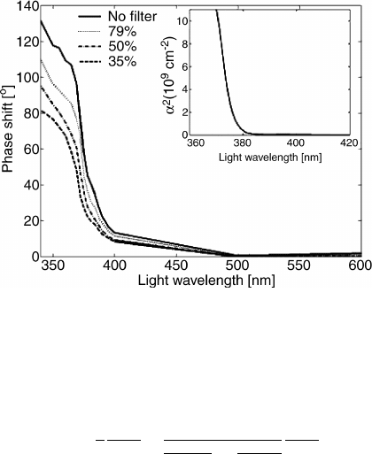
The phase shift at center frequency for the Sezawa wave mode with respect to the dark
condition, as a function of light wavelength and power level, is shown in Figure 11.22. The
inset shows the transmission spectrum of ZnO epilayer grown on r-Al
2
O
3
for comparison.
The UV SAW device response closely follows the absorption spectrum. For light
wavelengths above 400 nm, the phase shift is sma ll. The phase shift increases rapidly
as the light wavelength approaches the band edge at about 372 nm. The phase shift at
365 nm for a light power of 2.32 mW cm
2
is 107
, corresponding to a frequency shift of
1.36 MHz in an oscillator circuit, calculated for the standard oscillator circuit configura-
tion with the SAW in the feedback path:
Figure 11.21 Frequency response of the SAW UV detector under 365 nm light illumination,
under dark, 0.81 mW cm
2
and 2.32 mW cm
2
conditions. Reprinted from N. W. Emanetoglu,
et al., Surface acoustic wave ultraviolet photodetectors using epitaxial ZnO multilayers grown
on r-plane sapphire, Appl. Phys. Lett. 85, 3702 (2004)
310 ZnO-Based Ultraviolet Detectors
Df ¼
1
t
Df
360
o
¼
1
L
mesa
v
SAW; mesa
þ
L
IDT
v
SAW; IDT
Df
360
o
ð11:21Þ
where t is the delay time across the device, n
SAW,mesa
the acoustic velocity in the mesa
region, n
SAW,IDT
the acoustic velocity in the IDT region, L
IDT
the delay path length in the
IDT region, and Df the phase shift across the device. The Sezawa wave velocity in the
mesa region, v
SAW,mesa
, is estimated to be 5430 m s
1
. This 1.36 MHz frequency shift
corresponds to a 0.19% relative shift for a light power of 2.32 mW cm
2
, which compares
favorably with the 0.46% relative frequency shift at 40 mW cm
2
reported for a ZnO/LiNbO
3
SAW UV detector.
[82]
The estimated effective coupling, k
eff
2
,athf¼1710 is 1.6%, calculated
using the transfer matrix method. It is estimated that the maximum effective coupling that
could be obtained for this structure is 3.2% at hf ¼2820. Thus, device performance can be
improved by operating at a higher frequency using a smaller SAW wavelength.
Figure 11.23 shows the differential insertion loss for the Sezawa wave mode with
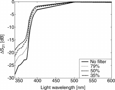
respect to the dark condition, as a function of light wavelength and power density. The data
have been normalized for constant power on the device. As the light wave approaches the
band edge, at about 372 nm, the differential insertion loss rapidly increases, similar to the
phase shift changes. At 365 nm, the differential insertion loss for the Sezawa mode under
2.32 mW cm
2
illumination is 22.8 dB.
11.3.3.3 Hybrid ZnO/LiNbO
3
SAW UV Photodetector
UV photodetectors have been developed by combining various SAW devices, such as SAW
filter,
[82]
SAW oscillator
[84]
and SAW delay line,
[85]
with a ZnO photoconductor. In the ZnO/
LiNbO
3
hybrid photodetector, semiconducting ZnO is used as a photosensitive layer and bulk
LiNbO
3
is used to excite the SAW. A hybrid ZnO/LiNbO
3
SAW UV photodetector has
piezoelectric coupling.
[82]
The LiNbO
3
substrate was used for SAW excitation, while the
Figure 11.22 Phase shift vs light wavelength for light power of 2.32, 1.83, 1.18 and 0.81 mW
cm
2
. The responses have been normalized for constant power with respect to 365 nm. The
inset shows the absorption spectrum of a ZnO thin film on r-Al
2
O
3
. Reprinted from N. W.
Emanetoglu, et al., Surface acoustic wave ultraviolet photodetectors using epitaxial ZnO
multilayers grown on r-plane sapphire, Appl. Phys. Lett. 85, 3702 (2004)
ZnO Film-Based UV Photodetectors 311
unbalanced RF-magnetron sputtering deposited ZnO film was used as the photosensitive
layer. This device was reported to exhibit a frequency shift of 170 kHz at 37 MHz, for a UV
light intensity of 40 mW cm
2
. The wavelength of the UV light is 365 nm.
In order to enhance the UV sensitivity, a ZnO/LiNbO
3
SAW oscillator configuration
was used.
[84]
An Amplifier oscillator circuit was built up to improve the UV sensitivity.
The UV sensitivity was evaluated by both of the oscillation voltage amplitude and
frequency shift due to the acoustoelectron interaction described in Section 11.3.3.1. For
the amplitude measurement, the UV sensitivity depended on the power supply V
cc
of the
oscillator circuit and an oscillat ion quench was observed with a higher UV light intensity.
Kumar et al.
[84]
demonstrated a ZnO/LiNbO
3
UV detector by sputtering a thin layer of
ZnO film on a commercially available 128
Y-X LiNbO
3
SAW filter. The thickness of ZnO
was optimized to 71 nm to reduce the mass loading effect. The ZnO/LiNbO
3
UV-SAW
photodetector was connected into the positive feedback loop of a high frequency amplifier
to form an oscillator. By control of the power supply voltage, the UV detector exhibits a
UV sensitivity of 450 nW cm
2
and a voltage responsivity of 24 kV W
1
. For the
frequency evaluation, there was 28 kHz oscillation frequency (f
o
¼35.4 MHz) down
shift when UV illumination (34 mWcm
2
) was chopped after 5 s.
An UV array detector has been developed by introducing a LiNbO
3
-based slanted finger
interdigital transducer (SFIT) and multiple ZnO optically active areas deposited by RF
sputtering.
[86]
A SFIT can be treated as a combination of numerous subfilters, each with a
uniform finger width and with a distinct center frequency. Figure 11.24 shows a schematic
structure of a SFIT SAW UV array detector. The ZnO-based optically active areas are
designed perpendicular to the SAW propagation direction between two ports of the SFIT
electrode. Therefore, the SAW response introduced by each active area is distinguishable
from the operating frequency. The magnitude of the corresponding frequency is related to
the UV light intensity due to the acoustoelectric interaction between the SAW and
photogenerated carriers in the ZnO photoconductive overlayer. When the size of an optical
active area is reduced, the spatial distribution of the light field can be detected and recorded.
Figure 11.23 Differential insertion loss vs light wavelength for light power of 2.32, 1.83, 1.18
and 0.81 mW cm
2
. The responses have been normalized for constant power with respect to
365 nm. Reprinted with permission from J. Zhu
312 ZnO-Based Ultraviolet Detectors