Litton C.W., . Reynolds D.C., Collins T.C. Zinc Oxide Materials for Electronic and Optoelectronic Device Applications
Подождите немного. Документ загружается.

levels in the energy gap. The depletion layer is extended from the surface into the bulk due
to generation of electron trapping in these surface states. The extended built-in electric
field effectively separates electrons from holes, leading to increased photoexcited carrier
lifetime for a higher photoresponsivity. On the other hand, on the Zn-face, the built-in
electric field only exists near the surface; therefore the surface recombination is fast.
Particularly, at shorter wavelength than the absorption band edge, the surface absorption
and recombination dominates for the Zn-face ZnO.
11.2.1 Persistent Photoconductivity
Persistent photoconductivity (PPC) has been observed in various types of ZnO, including
polycrystalline,
[38,40]
epilayer,
[61,62]
and nanowires (NWs).
[63,64]
PPC is closely related to
the slow photoconduction process. It has been reported that polycrystalline ZnO samples
show a very slow relaxation (over a time interval of hours or days) of conductivity after
illumination.
[36–38,40]
PPC is associated with the defects in semiconductor materials, such
as neutral donor (DX) centers in III–V alloys. Under the light illumination, these DX
centers can transfer between a nonconducting defe ct loca lized state (DLS) in the band
gap and a conducting DLS resonant with the conduction band, which is a delocalized
hydrogenic-like state,
[65]
giving rise to PPC in the semiconductors.
A slow photoresponse component dominates the photoresponse of ZnO photodetectors
when PPC is present. In a PPC process, photogenerated holes are usually captured by the
hole traps, resulting in a reduced electron–hole recombination rate and an increased
lifetime of nonequilibrium electrons. Therefore, a large photoconductive gain is expected
to accompany PPC. The presence of PPC dramatically affects the performance of ZnO-
based UV photodetectors by reducing the UV/visible rejection ratio and decreasing the
photoresponse speed.
The influence of grain boundaries on photoconductivity of polycrystalline ZnO was
studied by Zhang.
[40]
The photoresponse is related to the changes of barrier heights of
grain boundaries when the films are irradiated with UV light. It is suggested that the hole
traps contributing to the pers istent photoconductivity are located at grain boundaries.
Several defect related photoconduction mechanisms have been proposed. Tomm et al.
observed that room temperature photocurrent peak is significantly below the room
temperature band edge in the ZnO films grown by laser-assisted molecular beam epitaxy
(MBE).
[42]
It is suggested that the photoconduction process is defect related. However, the
nature of the defects is unclear.
Zhang et al. proposed a two-hole capture model through the oxygen vacancy (V
O
)to
explain the slow photoconductivity decay.
[66]
The energy levels of the intrinsic defects in
ZnO were calculated by the local density approximation (LDA) method. They found that
the þ2 charge ionized oxygen vacancy had a lower energy than a charge neutral V
O
due to
a large lattice distortion formed after capturing two holes. Therefore, a charge neutral
oxygen vacancy can capture two holes. The reduction of delocalized holes causes a
decrease of electron–hole recombination rate, which is responsible for the fast photo-
conduction decay. A fast phonon-assistant conductivity relaxation is suppressed because
of the deep energy level from the hole traps and large lattice distortion. As a result, a slow
process dominates.
Photoconductivity in ZnO 293
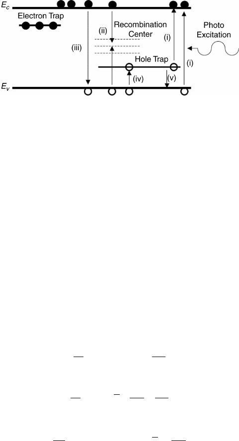
Moazzami et al. studied the sub-band-gap photoconductivity in n-type ZnO films grown
by plasma-assisted MBE on c-plane sapphire.
[49]
The carrier trapping dynamics were
investigated by time-resolved photoluminescence (PL) and photoconductive transient
under optical excitation wavelengths of 400–700 nm. Figure 11.5 illustrates a proposed
model for PPC in ZnO involving hole traps and defect levels.
Under an optical excitation, electron–hole pairs are generated, either between the defect
states and the band edge, or between the conduction band (CB) and the valence band (VB).
The PPC could be attributed to the capture of holes in the hole trap states, followed by hole
emission and carrier recombination. A deep hole trap may act as a negative charge when it
is filled with a hole, similar to the hole trap observed in GaN. The excess hole captured by
the hole traps are thermally emitted into the VB, and recombine with the electrons in the
CB. A rate equation model describes the persistent photoconductive process in n-type
ZnO:
[49]
dn
dt
¼ fsðN
T
NÞ
p
t
rec
ð11:5Þ
dp
dt
¼ Nse
E
p
kT
p
t
cap
p
t
rec
ð11:6Þ
dN
dt
¼ fsðN
T
NÞNse
E
p
kT
þ
p
t
cap
ð11:7Þ
where n and p are the electron and hole density in the CB and VB, respectively, N
T
is the
total density of hole traps, N is the number of filled hole traps, f is the incident photon flux,
s is the photon capture cross-section of the hole traps, t
rec
is the band edge carrier
recombination lifetime, t
cap
is the hole capture lifetime, E
p
is the energy separation
between the hole trap state and VB and s is the hole escape frequency.
In order to derive the trap density spectrum, assuming the hole capture lifetime is
much larger than the band edge carrier recombination lifetime, the relationship between
Figure 11.5 Schematic illustration of a proposed model for persistent photoconductivity in ZnO
involving hole traps and defect levels: (i) photogeneration of electron–hole pair; (ii) recombination
through recombination centers in the mid gap; (iii) band-to-band recombination; (iv) hole capture
process; and (v) hole emission process through hole traps. Adapted from K. Moazzami, et al., Sub-
bandgap photoconductivity in ZnO epilayers and extraction of trap density spectra, Semicond. Sci.
Technol, 21, 717 (2006)
294 ZnO-Based Ultraviolet Detectors

hole traps and conduction band electrons based on the rate equations is derived from
Equations (11.5)–(11.7):
ð
N
T
ðE
i
Þexpðse
E
i
kT
tÞdE ¼ DnðtÞð11:8Þ
where i represents the ith hole trap state.
Lany and Zunger proposed that oxygen vacancies act as a source of PPC in n-type ZnO
through the first-principle electronic structure calculations.
[67]
They suggested that the
neutral oxygen vacancy V
0
O
is a localized ground state in the energy band gap; however, the
ionized 2þexcited state V
2 þ
O
becomes an excited state resonant with the conduction band.
In this model, the light induced charge state transition follows:
V
0
O
!V
2 þ
O
þ2e ð11:9Þ
which leads to the configuration change for the oxygen vacancy from the nonconducting
ground to the conducting excited state. To return to the ground state, the metastable state
needs to be thermally activated across an energy barrier while an electron must be captured
by the DLS from the CB, as a result, n-type PPC occurs.
Reemts and Kittel suggested that PPC in highly porous ZnO films could be attributed to
a lattice relaxation process of surface states, when electrons are photoexcited into the
surface states located in the energy band gap of ZnO.
[68]
A stret ched exponential law was
used to fit the photores ponse decay.
11.2.2 Negative Photoconductivity
Negative photoconductivity has been observed in ZnO NW assemblies [such as compo-
sites of ZnO-AA M (anodic alumina membrane) and ZnO-CNT (carbon nanotubes)].
[69,70]
The potential applications include optical logic circuits and high-resolution image sensors
for integrated nanoscale optoelectronics.
Sen et al. studied the negative photoconduction in a planar two-dimensional network
consisting of ZnO particles (with diameters of 0.1–100 mm) and single-walled carbon
nanotubes (ZnO-CNT).
[69]
Under UV light illumination (340 nm, 10 mW cm
2
), the
conductivity of ZnO-CNT decreased by 3% compared with the dark value. An intensity-
dependent photocurrent was obtained on ZnO-CNT devices and fitted to a double
exponential decay with characteristic time constants of 450 and 75 s, respectively.
The negative photoconduction is attributed to the interface-mediated charging/dischar-
ging effect involving oxygen chemisorption/desorption on the surface of ZnO particles
that form a heterojunction with CNTs. The exponential photocurrent decay is explained
by the surface charge stated modified band energy diagram at the ZnO/CNT interface,
approximately follows:
Dn
s
I
p e
E
v
E
F
=kT
E
V
I
ð11:10Þ
Photoconductivity in ZnO 295
where Dn
s
is the surface charge density, I is the light intensity, E
V
is the position of the
valence band, and p is the effective hole concentration.
Transition from negative photoconductivity to positive photoconductivity in ZnO
NWs was realized through thermally annealing AAM as the NW growth template.
[70]
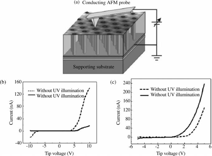
High density vertical ZnO NW arrays were grown in AAM by laser-assisted chemical
vapor deposition (CVD) [Figure 11.6(a)]. Before the CVD growth, Sn catalyst was
deposited by electrochemical deposition into the bottom of the AAM channels. As
shown in Figure 11.6(b), negative photoconductivity is observed in the ZnO NW. It
is expected that the anion impurities introduce electron trapping in the inner alumina
layer. Since ZnO NW and the inner AAM channel forms a core–shell heterostructure,
electrons can tunnel into these trapping states above the conduction band upon
photoexcitation, lowering the conduction electron concentration in the NW. When an
AAM was thermally annealed at 500
C for 13 h in pure argon gas, positive photocon-
ductivity is observed [Figure 11.6(c)]. This is attributed to thermal d ecomposition of the
acid anion and thus reduction of the im purity levels in the alumina.
Figure 11.6 (a) Schematic illustration of an atomic force microscopy (AFM) probe to
measure individual ZnO NWs in a vertical NW array. (b) I–V curves measured from a single
ZnO NW in an unannealed AAM, showing negative photoconductivity. (c) I–V curves
measured from a single ZnO NW in an annealed AAM, showing positive photoconductivity.
Reprinted from Z. Fan, et al., Electrical and photoconductive properties of vertical ZnO
nanowires in high density arrays, Appl. Phys. Lett. 89, 213110. Copyright (2006) with
permission from American Institute of Physics
296 ZnO-Based Ultraviolet Detectors
11.3 ZnO Film-Based UV Photodetectors
11.3.1 Photoconductive UV Detector
The photoconductive photodetector is the simplest device, acting as a photo-sensitive
resistor. When an incident photon has energy higher than the band gap energy of ZnO,
an electron–hole pair is produced. The electron and hole are separated under the electric field.
The photogenerated current is collected by the electrodes of the samples under the proper
bias. The photoconductive UV detector exhibits an internal photoelectric gain. However, the
photoconductive type of detector has the limitation of the gain-bandwidth. The ZnO film
thickness should be optimized so that the ZnO layer can absorb sufficient incident photons
without producing a large noise current due to the ZnO intrinsic conductivity. The circular or
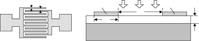
interdigital (IDT) metal pattern is deposited on top of the ZnO surface for the electrode.
Figure 11.7 shows the schematic diagram of a ZnO IDT MSM photoconductive photode-
tector on a sapphire substrate; Figure 11.7(a) is the top view and (b) the cross-sectional view.
Photoconductivity in polycrystalline ZnO films has been reported extensive-
ly.
[14,16–18,36]
Polycrystalline ZnO films were deposited by RF sputtering,
[17,40,71]
ion-
beam sputtering,
[16]
and solution-based synthesis,
[14,36]
etc. While exhibiting large
photoresponse, the photodetector mad e of polycrystalline films suffers from slow speed
and large noise due to the dark conductivity.
Liu et al. reported the first epitaxial a-plane ZnO film-based UV photoconduc tivity
detector.
[19]
In comparison with its polycrystalline counterpart, the epitaxial ZnO-based
detector significantly improves the photoresponse time. The photodetector is made of a
1 mm thick a-plane ZnO epitaxial layer grown on r-plane sapphire using metal organic
chemical vapor deposition (MOCVD). Diethylzinc (DEZn) and oxygen were used as the
Zn metal organic source and oxidizer, and NH
3
was used as an in situ dopant for MOCVD
growth. The typical growth conditions were the following: chamber pressure of 50 Torr,
10–15 lpm of N
2
(carrier gas), 1000 sccm of O
2
, DEZn bubbler temperature of 10
C,
100 sccm Ar flow through DEZn bubbler, growth temperature in the range of 350–600
C.
Growth rates of 1–2 mmh
1
were obtained. Unintentionally doped ZnO generally exhibits
n-type behavior because of the presence of various defects such as oxygen vacancies, zinc
interstitials and impurities. In order to reduce the background electron concentration, the
compensation doping process, such as in situ nitrogen doping, was carried out by
introducing NH
3
during MOCVD growth of ZnO.
c
d
Sapphire Substrate
Light Illumination
ZnO
Al
Al
d
c
t
(a) (b)
Figure 11.7 Schematic drawing of a ZnO IDT MSM photoconductive photodetector on a
sapphire substrate. (a) Top view and (b) cross-sectional view, where c and d are the metal
electrode finger width and interelectrode spacing, respectively, and t is the thickness of the
ZnO film
ZnO Film-Based UV Photodetectors 297
The ZnO films deposi ted on (01
12) Al
2
O
3
with their (11
20) a-plane parallel to the
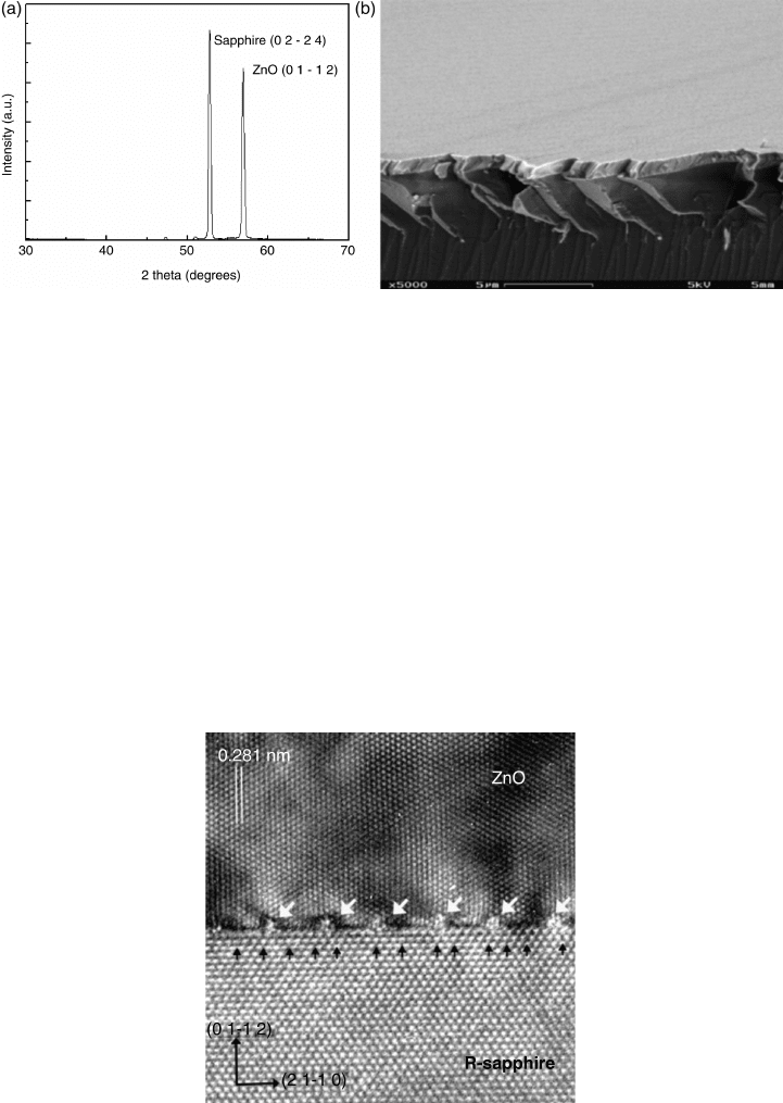
surface, as confirmed by the X-ray diffraction (XRD) u–2u scans [Figure 11.8(a)]. The in-
plane orientation of the films was analyzed by X-ray f-scans, and the epitaxial relation-
ship was determined to be (11
20) ZnO//(01
12) Al
2
O
3
and [0001] ZnO//[0
11 1] Al
2
O
3
.
[72]
The lattice mismatch parallel to and perpendicular to the [0001] dir ection of ZnO is 1.53
and 18.3%, respectively. The a-plane ZnO films grown on r-sapphire are dense with a
smooth surface, as seen in the SEM image shown in Figure 11.8(b). A cross-sectional high
resolution transmission electron microscopy (HR-TEM) lattice image of the interface
between ZnO and r-sapphire is observed to be atomically sharp and semicoherent, as
shown in Figure 11.9.
Figure 11.8 (a) X-ray u–2u scan of ZnO on r-plane sapphire and (b) SEM image of the surface
morphology of ZnO films grown in the presence of NH
3
. Reprinted from Y. Liu, et al., J.
Electron. Mater, 29, 69. Copyright (2000) with permission from TMS
Figure 11.9 HR-TEM image of the interface between ZnO and r-sapphire. The view is along
the c-axis of ZnO. Highly strained regions with a repeat distance twice that of the misfit
dislocations are observed. Reprinted from C. R. Gorla, et al., J. Appl. Phys. 85, 2595. Copyright
(1999) with permission from American Institute of Physics
298 ZnO-Based Ultraviolet Detectors
UV photodetectors were fabricated based on MSM circular structures. The device material
is made up of 1-mm-thick N-doped ZnO grown on r-sapphire. Al (200 nm thick) was used as
the contact metal. A circular pattern was used for contact electrodes. The spacing of the two
electrodes varied from 2 to 16 mm. e-beam evaporation, photolithography and wet chemical
etching techniques were used to generate the metal electrode patterns. The spectral
photoresponse of the MSM photodetectors was measured using a 75 W Xe lamp UV light
source, an Oriel monochromator for monochromic light power output, and a chopper to
generate the light pulse with a frequency ranging from 1 to 1000 Hz. A Newport 1830-C
optical power meter was employed to calibrate the light beam intensity. I–V characteristics
were measured using a Tektronics Semiconductor Work-Bench 372.
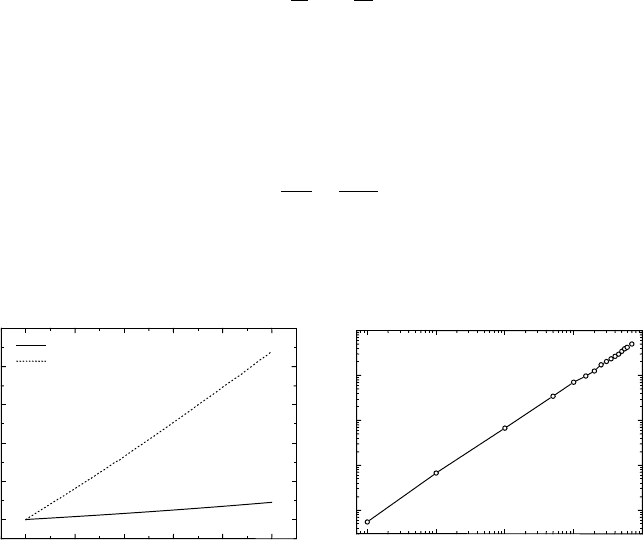
The mea sured dark and photoilluminated I–V char acteristics are shown in Figure 11.10
(a). The dark current for a bias voltage of 5 V was only 450 nA. The reason for relatively
low dark current is that the resistivity of the ZnO film was high. From the I–V measurement
data, we calculated the resistivity of the ZnO film to be 3.1 10
5
W cm. The wavelength of
365 nm was used for the photoilluminated I–V measurements. The light power was 6.4 nW.
The linear I–V relationships under both forward and reverse bias exhibit ohmic metal–-
semiconductor contacts. The detector operates in the photoconductive mode.
The gain of the photoconductor can be expressed as the following:
G
ph
¼
t
p
t
tr
ð1 þ
m
p
m
n
Þð11:11Þ
where t
p
is the effective recombination time for excess minority carriers, t
tr
is the transit
time of electrons in the device, m
n
and m
p
are the electron and hole mobilities, respectively.
t
p
can be much larger than t
tr
if the device is properly designed.
For the case of constant mobility when the bias V
b
is small, the photoconductor gain
G
ph
/ V
b
, the electron transit time can be expressed as:
t
tr
/
d
m
n
E
/
d
2
m
n
V
b
ð11:12Þ
where E is the applied electric field at low bias voltage V
b
.
012345
0
1
2
3
4
5
Dark Current
With photo-illumination:
P
ph
= 6.4 nW, λ = 365 nm
Current (μA)
10
-3
10
-2
10
-1
10
0
10
1
10
-1
10
0
10
1
10
2
10
3
λ = 365 nm
Optical Power = 6.4 nW
Photoresponsivity (AW)
Voltage (V)Voltage (V)
(a) (b)
Figure 11.10 (a) Dark (solid line) and photoilluminated (dashed line) I–V characteristics from a
ZnO MSM photoconductive photodetector and (b) photoresponsivity vs bias voltage of a ZnO
MSM photoconductive photodetector.ReprintedfromY.Liu,etal.,J.Electron.Mater,29,69(2000)
ZnO Film-Based UV Photodetectors 299
As shown in Figure 11.10(b), the photoconductors show a linear photoresponse vs
bias voltage from 1 mV to 5 V. Such a linear relationship indicates that the device
operates in the constant mobi lity range. For d ¼10 mm, l ¼365 nm, G
ph
/V
b
is approxi-
mately 120 V
1
.Assumingm
n
100 cm
2
V
1
s
1
m
p
, the m inority carrier lifetime (t
p
)
can be estimated as:
t
p
G
ph
d
2
m
n
V
b
1:2 10
6
s ð11:13Þ
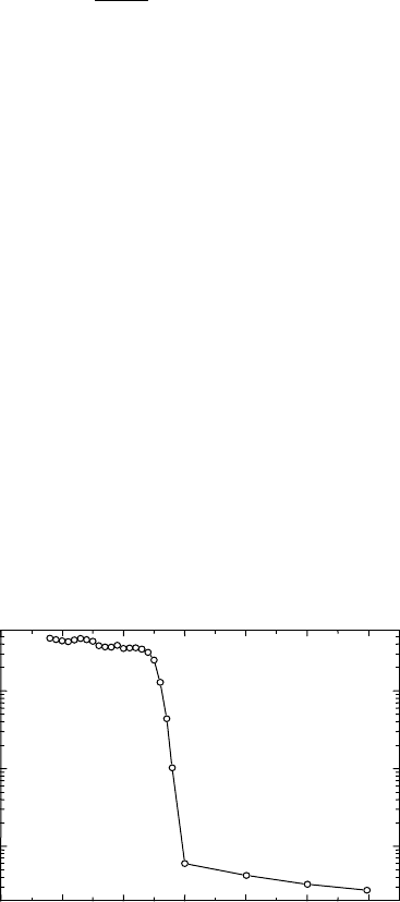
Figure 11.11 shows the spectral response of a MSM photoconductive detector. A sharp
cut-off near 373 nm was observed. The photoresponse drops by more than two orders of
magnitude across the cut-off wavelength within 15 nm of the band edge. These results are
consistent with the transmission measurements. There is a long absorption tail below the
band gap. The impurity levels within the band gap might be the source of the tail.
Photoresponsivity of about 400 AW
1
is obtained under 5 V bias.
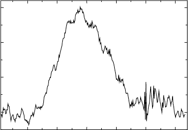
We have also measured the photoresponse speed of the detector. The optical excitation
source was a Ti:sapphire regenerative amplifier-pumped optical parametric amplifier,
which produces visible ultra short pulses at a 175 kHz repetition rate. These pulses were
compressed to less than 100 fs and frequency doubled in b-barium borate (BBO) to obtain
UV pulses tunable between 300 nm and 375 nm. Neutral density filters are used to control
the optical power on the detector. Shown in Figure 11.12 is the transient photoresponse of
the ZnO detector under 5 V bias. The rise time is about 1 ms, while the fall time is about
1.5 ms.
The fast photoresponse of the photoconductors can be attributed to the improvement of
the crystalline quality of the ZnO films, which reduces the defect-induced recombination.
Simultaneously, the oxygen adsorption process is suppressed by reducing the electron
carrier concentration (by N doping) and by greatly reducing the grain boundaries in the
high-quality epitaxial ZnO film.
550500450400350300250
1
10
100
Bias = 5 V
Photoresponsivity (A/W
-1
)
Wavelen
g
th (nm)
Figure 11.11 Spectral response of a ZnO MSM photodetector under 5 V bias. Reprinted from
Y. Liu, et al., J. Electron. Mater, 29, 69 (2000)
300 ZnO-Based Ultraviolet Detectors
11.3.2 Schottky Barrier UV Photodetectors
The Schottky barrier photodetector is among the simplest of the unipolar photovoltaic
devices. Under optical illumination, the nonequilibrium minority carriers generated in the
bulk of the semiconductor are collected by the built-in electrical field of the Schottky
barrier formed at the semiconductor surface. The advantages of Schottky photodiodes are
high speed, low noise performance, and ease of fabrication. Fabricius et al. made Schottky
barrier type UV sensitive photodiodes using Au on a thin sputtered layer of polycrystalline
ZnO.
[13]
These photodiodes exhibited slow operating speed (rise time 20 ms and decay
time 30 ms) and low quantum efficiency (1%) due to the large amount of recombination
centers in the polycrystalline ZnO layers.
The first Schott ky barrier photodetector based on epitaxial ZnO film was repor ted by
Liang et al. a t Rutgers.
[20]
In this work, the Schottky barrier UV photodetector is made
of nonpolar (11
2 0) a-plane ZnO epitaxial films grown by MOCVD. As described in
Section 11.3.1, the epitaxial relationships between a-plane ZnO and r-plane sapphire
substrate were determined to be (11
20) ZnO//(01
12) Al
2
O
3
and (0001) ZnO//(0
111)
Al
2
O
3
. There fore, t he c-axis of ZnO lies in the surface p lane (11
20) of the ZnO film. In
this nonpolar a-plane, absence of n et surface charges (due to the presence of equal
numbersofbothZnaswellasOatomsonthesurface)andanetzerodipolemoment
normal to the surface prevent diverg ence of surface energy.
[73–75]
As a result, Schottky
contacts formed on a-plane ZnO surfaces would be more stable as compared with the
polar c-plane surface. Furthermore, in this a-ZnO/r-Al
2
O
3
system, the lattice mismatch
between ZnO and the substrate along the c-axis is 1.53%, while along the directi on
perpendicular to the c- axis is 18.3%. The overall lattice mismatch is less than that of the
polar (0001) ZnO film on c-plane sapphire system.
a-plane ZnO epitaxial films were grown on r-plane (01
12) sapphire substrates in a low-
pressure MOCVD reactor. DEZn and O
2
were used as the source materials. The reactants
were introdu ced in the reactor by two separate injectors to reduce gas phase reaction. The
DEZn flow rate was 50–100 sccm and the O
2
flow rate was 1000–2000 sccm. The growth
012345
0
1
2
3
Photocurrent (nA)
Time (
μ
s)
Figure 11.12 Photocurrent transient of a ZnO MSM photodetector. Reprinted from Y. Liu,
et al., J. Electron. Mater, 29, 69 (2000)
ZnO Film-Based UV Photodetectors 301

temperature range was from 380 to 420
C. The typical growth rate was 1–2 mmh
1
.
Because unintentionally doped ZnO film prepared by MOCVD generally exhibits n-type
conduction due to oxygen vacancies or Zn interstitials, NH
3
(500 sccm) was used as a
nitrogen compensation doping source to reduce the electron concentration. A 500 nm ZnO
epilayer was grown with carrier concentration of about 10
16
cm
3
.
UV photodetectors were designed and fabricated using both circular and IDT MSM
structures. For the circular structure, the outer diameter is 320 mm, the inner diameter is
150 mm, and the gap is 10 mm. For the IDT structure, the fingers are 10 mm wide and
180 mm long, with a 10 mm gap. Aluminum and silver were used to form ohmic and
Schottky contacts, respectively. The formation of Schottky contacts is greatly influenced
by chemical reactions at the metal and semiconductor interface and diffusion of the metal
into the semiconductor. This effect is much more pronounced for II–VI oxides as
compared with III–V nitrides. In the case of ZnO, the less reactive metal Ag is used
to form Schottky contacts for the UV photodetectors. The Ag-ZnO-Al circular structures
were used for Schottky diode studies, while the Ag-ZnO-Ag structures served as Schottky-
type MSM photodetectors. For comparison, the Al-ZnO-Al structures were also fabricated
as MSM photoconductive detectors. e-beam evaporation was utilized for metal deposition.
The thickness of Al and Ag layers was 2000 A
. For the Schottky contact, a 500 A
thick Au
layer was finally deposited on the top of the Ag layer, to act as an oxide-resistant layer. It is
well known that in fabrication of Schottky contacts, the surface states, contaminants and
defects of the surface layer significantly affect the barrier height and leakage current.
Oxygen plasma was used to clean the surface before and after the metallization process in
order to minimize such effects.
Photoresponse measurements were performed using an Oriel optical system. The
photoresponse speed of the detector was also measured. The optical excitation source
was the 337.1 nm line of a N
2
pulse laser, with a pulse width of 2 ns at a repetition rate of
40 Hz. A Xe arc lamp and monochromator combination provided the light source. The
signal from the detector was monitored by a lock-in amplifier. Neutral density filters were
used to control the optical power on the detector. Optical energy on the detector was about
10 nJ per pulse. The signal from a 50 W load resistor was recorded by a digital scope with a
time resolution better than 1 ns. The bias voltage was 9 V.
Shown in Figure 11.13 are the I–V characteristics of ZnO MSM circular devices,
including both Schottky and ohmic types. The linear I–V relationship from the Al-ZnO-Al
structure clearly indicates the ohmic behavior of the Al on n-type ZnO contact. On the
other hand, the rectified I–V relationship from the Ag-ZnO-Al confirms Schottky junction
formation between Ag and n-type ZnO. In a Schottky diode, the general I–V characteristics
are represented by:
J ¼ J
o
expð
qV
ZkT
Þ1
; ð11:14Þ
J
o
¼ A
T
2
expðF
B
=kTÞ; ð11:15Þ
where J
o
is the saturation current density, Z is the ideality factor, k is Boltzmann’s constant,
T is the absolute temperature, A
is the effective Richardson coefficient, and F
B
is the
barrier height. The Schottky contact area is 1.77 10
4
cm
2
. The values of Z ¼1.50 and
302 ZnO-Based Ultraviolet Detectors